Radiated Emission of a Bent Microstrip Line Using Hertzian Dipole Method
Yee See Khee, Mohd Zarar Mohd Jenu
Center for Electromagnetic Compatiblity, Universiti Tun Hussein Onn Malaysia, 86400 Parit Raja, Batu Pahat, Johor, Malaysia [email protected], [email protected]
Abstract - Electromagnetic Interference (EMI) and
Signal Integrity (SI) issues have generated challenges to the high speed digital circuit designer as the operating clock frequency of the system continue to increase to accommodate broadband applications. Discontinuity due to microstrip bents which appear frequently in most VLSI design requires thorough understanding on the current distribution in order to generate the immunity and emission characteristic of the circuit. This paper is on estimating the radiated emission on both the straight and bent microstrip line using the expanded hertzian dipole approach which will be validated with computer simulation results. It is found that the expanded hertzian dipole approach which is initially applied on wire [7] can predict the emission on microstrip line well when proper adjustment is made.
Keywords: Radiated emission; Microstrip; Hertzian Dipole Method
1.
Introduction
Nowadays, as the demand to accommodate the layout density, processing speed, more over the cost pressure continue to aggrandize, these implicitly drive the awareness on the simulation of the unintentional radiated emission of printed circuit boards (PCBs) in order to achieve a design-integrated electromagnetic compatibility analysis. Antecedent, less attention has been paid to the differential-mode radiation from the signal trace, adversely attention had been put on the other predominance radiation from common-mode current and power bus. Anyway, this situation changed as the clock speeds have reached the gigahertz range, differential-mode radiation has received a considerable emission potential.
The increasing speed of the digital circuits as well as the density of printed circuit board often results in more challenging signal integrity quandary. Bifurcated traces (T-junction, Y-junction, right-angle bends or left-angle-bended and steps planar transmission lines) are currently a compulsion to fulfil the needs of a denser printed circuit boards during the routing cycle. Discontinuity which contributes to the reflection and mismatching troubles is the culprit which always degrades the quality of the signal.
As a rule of thumb, one of the effective ways to reduce this type of emission is to route all the high-speed signal nets on the inner layer of the boards, shielded by solid ground or supply layers. Although this idea seem to be workable, it is not practical from the standpoint of cost reduction. So eventually, there will be some critical traces which fail to be shielded.
Previous work in this area has long attracted attention since early of 1960s. A lot of investigation has been carried out on this issue, including the optimisation of the bended trace to improve its performance by mitterring [2], [3], [6]. Other researchers prefer on the subject involving the radiation loss of the bent structure with different bent angle [4] – [7]. In this paper, focus will be put on the radiated emission of a bent microstrip line with bent angle of 90 degrees when it is matched, unmatched and open terminated with respect to the frequency range of 1 – 3 GHz.
Numerous approaches have been reported in the literature [4]-[7] to compute the radiation from the bent microstrip line. Hence different formulation to represent the electric field had been published. The formulation applied in this paper will be described briefly in section 2. Section 3 will include the simulation configuration while result and discussion will be examined in section 4.
2.
Calculation of Electric Field by
Hertzian Dipole Approach
The structure of the bent microstrip line in this paper is shown in Figure 1. A bent microstrip line with width of 2.93 mm is bent from the negative x axis toward the positive y axis with bent angle of φoat x = 0. The length of each arm is L, which is equal to 20 mm. A voltage source Vs with a source impedance of
Rs is attached to one end, and a load RL is attached to
the other end.
Figure 1: Structure of bent microstrip line
The Hertzian Dipole consists of an infinitesimal current element dl carrying a phasor current Iˆthat is
assumed to be the same (in magnitude and phase) at all point along the element length [1].
Radiating section in an electrical circuit are considered to be made up of a number of ideal radiating dipoles, short enough for the current to be approximated as constant along the length of each dipole.
For a single short dipole element of length l in free space (permittivity εo and permeability μo) with the
[image:2.595.299.526.129.674.2]coordinate system given in Figure 2, the radiated field can be obtained in the frequency domain as described in [8].
Figure 2: Hertzian Dipole and the Coordinate Systems
[image:2.595.71.265.622.746.2]The coordinate system to calculate the electric field radiated from a bent microstrip line with a bend angle of φo is illustrated in Figure 3 [7]. The bent microstrip line can be divided into a number of cascaded short uniform dipoles. The electric field from the entire bent wire can be found from the sum of all the contributions from each dipole element of the line.
Figure 3: Coordinate system to calculate the E field [7].
In frequency domain, the formulas to calculate the electric fields expanded from the hertzian dipole are shown as follows [7]:
( )
ξ,
ω
x dE(
) (
[
)
(
)
]
( )
( )( )
( )
( )
( )
( )
( )( )
( )
( )
ξ
ξ
ω
ξ
ω
ξ
πε
φ
ξ
ξ
ξ
ω
ξ
ω
ξ
ξ
πε
ξ
φ
φ
ξ
φ
φ
ξ
φ
ξ
ξ ω ξ ω d R c j R j R c e I d R c j R j R c R e I y x x o o c R j o o o c R j o o ⎥ ⎦ ⎤ ⎢ ⎣ ⎡ + + × − ⎥ ⎦ ⎤ ⎢ ⎣ ⎡ + + × × − + − × − = − − 2 0 3 2 / 2 3 2 2 / 1 1 4 cos 3 3 4 sin sin cos cos cos(
ξ,
ω
)
y dE
(
) (
[
)
(
)
]
( )
( )( )
( )
( )
( )
( )
( )( )
( )
( )
ξ
ξ
ω
ξ
ω
ξ
πε
φ
ξ
ξ
ξ
ω
ξ
ω
ξ
ξ
πε
ξ
φ
φ
ξ
φ
φ
ξ
φ
ξ
ξ ω ξ ω d R c j R j R c e I d R c j R j R c R e I y x x o o c R j o o o c R j o o ⎥ ⎦ ⎤ ⎢ ⎣ ⎡ + + × − ⎥ ⎦ ⎤ ⎢ ⎣ ⎡ + + × × − + − × − = − − 2 0 3 2 / 2 3 2 2 / 1 1 4 sin 3 3 4 sin sin cos cos sin( )
ξ,
ω
x dE
(
) (
[
)
(
)
]
( )
( )( )
( )
( )
( )
ξ
ξ
ω
ξ
ω
ξ
ξ
πε
ξ
φ
φ
ξ
φ
φ
ξ
ξ ω d R c j R j R c R e I y x h z o o o c R j o ⎥ ⎦ ⎤ ⎢ ⎣ ⎡ + + × × − + − × − = − 2 3 2 2 / 3 3 4 sin sin cos coswhere
(
) (
2) (
2)
2sin
cosφ ξ φ
ξ + − + −
−
= x z h y
R , I
( )
ξis the current at position ξ on the line, ω=2πf, f is the frequency, and co is the speed of light. In order to
obtain the total E field in each direction (Ex, Ey, and Ez),
we set φ = 0 for the first arm while φ =φo for the second arm. φo represents the bent angle of the structure as shown in Figure 3. The effect of the ground plane is included by the method of images.
In the preliminary state, I
( )
ξ is derived by using the phasor solution, assuming the source is a single-frequency sinusoidal waveform. The phasor current at any point on the line in terms of the source voltage is given as [1]:
( )
βξβ βξ β
ξ
j s c s L j L s j L j L e Z Z V e e e I − − − + Γ Γ − Γ −= 2 22
1
1 (4)
(1)
(2)
where ΓLand Γsare the load and source reflection coefficient respectively. Vs represents the phasor source
voltage, Zc and Zs are the characteristic impedance and
source impedance and ζ equate to each position on the line and β serve as the phase constant.
3.
Simulation Configuration
In the effort to validate the modelling result by using the expanded hertzian dipole approach, MICROWAVE STUDIO® has been utilized.
In this paper, the radiated emission at a distance of 0.1 m from the origin of 2 different type of structure will be investigated. First, a straight microstrip line and second a 90 degrees bent microstrip line. Both of them are separated from ground plane by dielectric layer of FR4. The input source is a 1W p-p signal, with 50 ohm of input impedance operating in frequency range of 1-3 GHz. They are investigated with 3 different conditions, matched (50 Ω), unmatched (10 Ω) and open termination.
In the first case, it is a straight microstrip line with dimension of 40 x 12 x 1.67 mm. The track is constructed with source injected from negative x axis direction and terminated at positive x axis direction. The total length of the signal trace is 40 mm.
On the other hand for the second case, it is a bent microstrip line with dimension of 40 x 40 x 1.67 mm. Similarly, the source is added from the negative x axis direction, but there is 90 degrees of bent when the track is extended up to origin, later on the track is continued back in the positive y axis direction. The length of each arm is 20 mm.
The result of the investigation will be presented in the next section.
4.
Result and Discussion
The radiated emission is represented by the two dimensional polar view. First of all, the required Cartesian coordinates x, y, z 0.1 m away from the origin can be converted from the spherical coordinateφ, θ, r by using the coordinate transformation.
Substituting the elements into equation (1) – (4), the electric field, Ex, Ey, Ez in the Cartesian frame can
be obtained. These fields are then converted to components Er,Eφ,Eθ in the spherical coordinate
system for plotting in the two dimensional polar views.
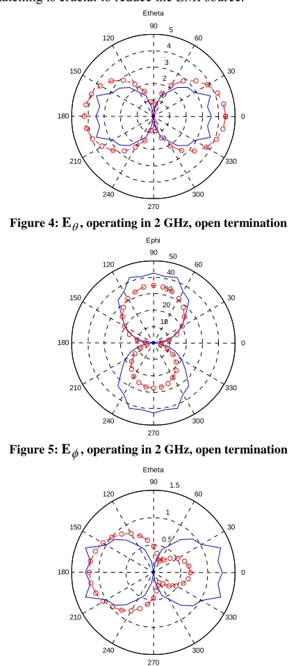
4.1 Straight Microstrip Line
Figure 4 – Figure 9 are the two dimensional radiation pattern of a straight microstrip line with different operating frequency and different termination scheme. The solid line represents the result from the expanded hertzian dipole approach, while the bubble line is the result simulated by using the MICROWAVE STUDIO®. From the observation, it is found that
generally, the radiation pattern and directivity of the electric field calculated by the expanded hertzian dipole approach is in agreement with the result achieve by the MICROWAVE STUDIO®.
According to [7] and [9], the radiation pattern is almost symmetric with respect to φ =φo/ 2. The θ
component radiates strongly in the directions of propagation of the current, for example φ = 0 and
φ =φo, and on the other hand, φ component radiate strongly into the intermediate direction. This condition is clearly illustrated in the results
Other than this, from the figure, it is found that, the radiation is stronger when the structure is not matched terminated. This implicitly proof that proper matching is crucial to reduce the EMI source.
1 2
3 4 5
30
210
60
240 90
270 120
300 150
330
180 0
[image:3.595.320.533.270.748.2]Etheta
Figure 4: Eθ, operating in 2 GHz, open termination
10 20
30 40 50
30
210
60
240 90
270 120
300 150
330
180 0
Ephi
Figure 5: Eφ, operating in 2 GHz, open termination
0.5 1 1.5
30
210
60
240 90
270 120
300 150
330
180 0
Etheta
5 10
15
30
210
60
240 90
270 120
300 150
330
180 0
[image:4.595.73.268.82.588.2]Ephi
Figure 7: Eφ, operating in 1 GHz, matched termination
1 2 3
4 5
30
210
60
240 90
270 120
300 150
330
180 0
Etheta
Figure 8: Eθ, operating in 3 GHz, unmatched termination
5 10
15 20 25
30
210
60
240 90
270 120
300 150
330
180 0
Ephi
Figure 9: Eφ, operating in 3 GHz, unmatched termination
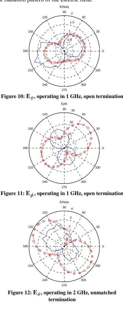
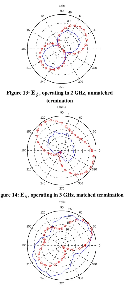
4.1 90 Degrees Bent Microstrip Line
In the second situation, it is a bent microstrip line with its bent angle of 90 degrees. Several two dimensional polar view of the structure are depicted in Figure 10 – Figure 15.
The comparisons of straight microstrip line show better result than the bent microstrip line.
Microstrip line with bent behave differently compare with straight microstrip line. The bending introduce impedance mismatch in between one section of the track (before the bent) with another section of track (after the bent). So in other words, the signal trace can no longer be represented with single
characteristic impedance, single source reflection coefficient and also single load reflection coefficient. Anyway, in expanded hertzian dipole approach presented in this paper, the conventional phasor current, I
( )
ξ (4) is substituted into equation (1) – (3), which is the main factor that cause the inaccuracy on the radiation pattern of the electric field.0.5 1
1.5 2
30
210
60
240 90
270 120
300 150
330
180 0
[image:4.595.309.514.165.692.2]Etheta
Figure 10: Eθ, operating in 1 GHz, open termination
10 20
30
30
210
60
240 90
270 120
300 150
330
180 0
Ephi
Figure 11: Eφ, operating in 1 GHz, open termination
1 2
3 4
30
210
60
240 90
270 120
300 150
330
180 0
Etheta
10 20
30 40
30
210
60
240 90
270 120
300 150
330
180 0
[image:5.595.81.298.83.573.2]Ephi
Figure 13: Eφ, operating in 2 GHz, unmatched termination
1 2 3 4
5
30
210
60
240 90
270 120
300 150
330
180 0
Etheta
Figure 14: Eθ, operating in 3 GHz, matched termination
5 10
15 20
25
30
210
60
240 90
270 120
300 150
330
180 0
Ephi
Figure 15: Eφ, operating in 3 GHz, matched termination
5.
Conclusion
Radiated emission estimated by using the expanded hertzian dipole approach [7] is compared with the simulation result of the MICROWAVE STUDIO®. Reasonable good agreement is achieved for the straight microstrip line. Although obvious differences are observed for the case of bent microstrip line, the main factor lead to the incorrectness is explained.
The result reveals that, the radiation pattern of the straight microstip line is symmetric with respect to the
φ =φo/ 2, the θ component radiates strongly in the directions of propagation of the current, for example
φ =0 and φ =φo, and on the other hand, φ component radiate strongly into the intermediate direction.
The future work will be concentrated in the effort in finding a more suitable equivalence to represent the current distribution in the bent microstrip line in order to assist circuit designer to improve on their circuit design to ensure sufficient immunity and limited radiated emission for compliances with electromagnetic compatibility regulations (CISPR, FCC, VDE etc).
Reference
[1] C.R.Paul, Introduction to Electromagnetic Compatibility, New York: Wiley, 1992.
[2] Rene J. P. Douville, and David S. James, “Experimental Study of Symmetric Microstrip Bends and Their Compensation” IEEE Transaction on Microwave Theory and Techniques, VOL, MMT-26, NO 3, pp 175-182, March 1978.
[3] Rakesh Chadha, and K. C. Gupta, “Compensation of Discontinuities in Planar Transmission Lines” IEEE Transaction on Microwave Theory and Techniques, VOL, MMT-30, NO 12, pp 2151-2156, December 1982.
[4] T.K.Sarkar and Z.A. Maricevic “Characterization of Power Loss From Discontinuities in Guided Structures” IEEE MTT-S International Microwave Symposium Digest, VOL 2, pp 613-616, 8-13 June 1997.
[5] Raj Mittra and M. Irsadi Aksun, “Estimation of Spurious Radiation from Microstrip Etches Using Closed-Form Green’s Function,” IEEE Trans. Electromagnetic Compatibility, vol. 40, no. 11, pp. 2063–2069, Nov. 1992.
[6] S. Lee and M. Hayakawa, “A study on the radiation loss from a bent transmission line,” IEEE Trans. Electromagnetic Compatibility, vol. 43, no. 4, pp. 618–621, Nov. 2001.
[7] Xilei Liu, Christos Christopoulos, band David W.P Thomas, “Prediction of Radiation Losses and Emission From a Bent Wire by a Network Model” IEEE Transaction on Electromagnetic Compatibility, VOL 48, NO 3, pp 476-484, August 2006.
[8] J.D.Kraus, Electromagnetics, 4rd ed. New York: McGraw-Hill, 1992.
![Figure 3: Coordinate system to calculate the E field [7].](https://thumb-us.123doks.com/thumbv2/123dok_us/8783946.905760/2.595.71.265.622.746/figure-coordinate-system-to-calculate-the-e-field.webp)