© 2016, IRJET | Impact Factor value: 4.45 | ISO 9001:2008 Certified Journal | Page 414
An Interleaved High Step-Up Boost Converter With Voltage Multiplier
Module for Renewable Energy System
Vahida Humayoun
1, Divya Subramanian
21 P.G. Student, Department of Electrical and Electronics Engineering, KMEA Engineering College, Edathala, Kerala, India
2 Assistant Professor, Department of Electrical and Electronics Engineering,KMEA Engineering College,Edathala, Kerala, India
---***---Abstract - This paper presents a high step up
DC-DC converter with voltage multiplier module. Through a voltage multiplier module composed of switched capacitors and coupled inductors, a conventional interleaved boost converter obtains high step-up gain without operating at extreme duty ratio. High boost dc-dc converters play an important role in renewable energy sources such as fuel energy systems, DC-back up energy system for UPS, high intensity discharge lamp and auto mobile applications. Renewable energy sources such as photovoltaic energy are available in both clean and economical due to new advancement in technology and use of good and efficient cells. The configuration of the proposed converter not only reduces the current stress but also constrains the input current ripple, which decreases the conduction losses and lengthens the lifetime of the input source. DC power can be converted into AC power at desired output voltage and frequency by using an inverter. The coupled inductors can be designed to extend step-up gain, and the switched capacitors offer extra voltage conversion ratio. Hence, large voltage spikes across the main switches are alleviated, and the efficiency is improved. The high step-up conversion may require two-stage converters with cascade structure for enough step-up gain, which decreases the efficiency and increases the cost. Thus, a high step-up converter is seen as an important stage in the system.
Key Words: Switched Capacitors, Coupled Inductors
bridge Inverters, Boost–fly back converter, high step-up, photovoltaic (PV) system, voltage multiplier module.
1. INTRODUCTION
Renewable energy sources such as photovoltaic energy are available in both clean and economical due to new advancement in technology and use of good and efficient cells. Solar energy is advantageous compared to any other renewable energy sources available. The efficient and fast growth in the field of solar energy result in Photovoltaic (PV) system design for various application with reliable operation and application for
more reliable and efficient operation. PV module represents the fundamental power conversion unit of a PV generator system. The output characteristics of PV module depends on the solar insolation, the cell temperature and output voltage of PV module. Since PV module has nonlinear characteristics, it is necessary to model it for the design and simulation of PV system applications.
© 2016, IRJET | Impact Factor value: 4.45 | ISO 9001:2008 Certified Journal | Page 415
Fig -1: Block diagram of the system
1.1 PV Panel
A PV array is a group of several PV cells which are electrically connected in series and parallel circuits to generate the required current and voltage. The characteristics have a current source region and a voltage source region. The impedance is low at voltage source region, whereas high at current source region. Solar radiation is an important factor determining the I-V characteristics, hence these factors are required for the designing and implementation of solar cell. The short circuit current increases with the increase in solar radiation and open circuit voltage decreases with increase in temperature for constant radiation on surface of the cell. Partial shading is a phenomenon occurring in solar cells causing several numbers of maximum power points. The diodes are provided for reducing the reverse currents caused due to the problems of partial shading. These reverse current causes heating on solar cells, affecting the efficiency and performance at higher temperatures.
The electrical system connecting to the photovoltaic system depends on cell temperature, also sudden change in weather condition result in varying solar irradiation on the surface. The output voltage and current varies with the change in these parameters. These will affect in tracking maximum power from the cell.
1.2 Maximum Power Point Tracking (MPPT)
MPPT technique is to extract maximum power from photovoltaic systems. MPPT maintains the operation of maximum power with efficient MPPT techniques and they differ in many aspects such as required sensors, complexity, cost, range of effectiveness, convergence speed, correct tracking etc. Hill Climbing Techniques are used for tracking maximum power. Here the PV system uses P & O algorithm because of simplicity, less time and
parameters requirement. The algorithm starts with setting the reference voltage and power of the module.
Perturbation and Observation method is a Hill climbing method. In this method the operating voltages are increased or decreased for attaining a maximum point of operating and it compares the present value with previous value in each cycle of perturbation. The perturbation value decrease or increase the value of power, then the voltages are adjusted for obtaining a maximum power point. The operating point shifts with the perturbation on voltages, with a step increase or decrease in the duty cycle of the converter connected. The operating point oscillates around the maximum point causing power loss is a disadvantage of this method of tracking power. The step size is decreased to reduce the oscillation around the operating point. If the power and voltage are increased comparing to the previous cycle, then increase the voltage in order to track maximum power from left of the curve. If the change in power is increased and change in voltage is decreased, then decrease the voltage to track MPP from right of the curve. If the change in power is decreased and change in voltage is increased, then also decrease the voltage to track the operating point back to MPP, which is moving away from maximum point.
2. OPERATING PRINCIPLES OF CONVERTER
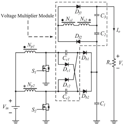
The step up converter is a non-isolated topology for boosting low voltage input to high voltage output. The input current is usually continuous in nature and is supplied to the load by either the conduction of diodes or capacitors. The boost converter with voltage multiplier by means of coupled inductor insertion increases the output voltage, hence the voltage gain and efficiency, with low value of duty cycle. The output voltage across the load is the sum of the voltage from boost converter and the voltage across the voltage multiplier capacitors. The required duty cycle can be obtained by adjusting the voltage multiplier, which increases the output voltage. The voltage multiplier module is composed of two coupled inductors and two switched capacitors and is inserted between a conventional interleaved boost converter to form a modified boost–flyback–forward interleaved structure.
© 2016, IRJET | Impact Factor value: 4.45 | ISO 9001:2008 Certified Journal | Page 416 and the other phase whose switch is in ON state
performs as a forward converter.
Fig -2: High step up converter with voltage multiplier
The equivalent circuit of the proposed converter is shown below, where Lm1 and Lm2 are the magnetizing inductors; Lk1 and Lk2 represent the leakage inductors; Ls represents the series leakage inductors in the secondary side; S1 and S2 denote the power switches; Cc1 and Cc2 are the switched capacitors; and C1, C2, and C3 are the output capacitors.
Fig -3: Equivalent circuit of High step up converter
When the switch S1 in the ON state, the magnetizing inductor, Lm1 is in the charging state. The reverse polarity of Lm2 causes diodes Dc2 and Db2
forward biased. Energy stored in Lm2 is transferred to the secondary side of the coupled inductor. The current through the series leakage inductor,Ls flows to the output terminal through the output capacitor C3 and flyback forward diode. When the switch S2 in the ON state, the magnetizing inductor, Lm2 is in the charging state. The reverse polarity of Lm1 causes diodes Dc1 and Db1 forward biased. Energy stored in Lm1 is transferred to the secondary side of the coupled inductor. The current through the series leakage inductor,Ls flows to the output terminal through the output capacitor C2 and flyback forward diode.
3. SIMULINK MODEL
The simulation is done on MATLAB simulink. The output of the PV system is connected to the boost converter and then to an inverter for connecting to ac loads. The simulink model of the system is shown below. The PV output voltage greatly governed by temperature while PV output current has approximate linear relationship with solar irradiances. Due to the high capital cost of PV array, MPPT control techniques are essential in order to extract the maximum available power from PV array in order to maximize the utilization efficiency of PV array.
[image:3.595.51.264.149.365.2]© 2016, IRJET | Impact Factor value: 4.45 | ISO 9001:2008 Certified Journal | Page 417
Fig -5: Input Voltage from PV Panel
The MPPT technique is simulated with the principle of P & O algorithm. The signal obtained from the algorithm are given to the gate of boost converter for the operation. The simulation model of the MPPT algorithm with P and O algorithm is shown below.
Fig -6: Simulink model of the MPPT
Fig -7:Gate Pulses to Switches
The high gain high step up converter with voltage multiplier is simulated on MATLAB software environment with photovoltaic system. The simulation was done with an input of 30-35 V supply to obtain an output of 300-400 V with combination of boost converter with voltage multiplier. The interleaved boost converter topology is designed for minimizing the switching losses and to improve the efficiency. The advantages of interleaved boost converters are to reduce current ripple and increases life of PV module. The capacitors C2 and C3 are designed for 220 µF and C1 for 470µF. The frequency is adjusted to 40 kHz by means of a pulse generator to obtain a gate pulse for the both the MOSFET switches. In the simulation of boost converter with voltage multiplier the voltage across load VL, voltage across switch VS, voltages across capacitors VC1, VC2 and VC3 are obtained. The design consideration of the high boost converter integration with voltage multiplier includes components selection and coupled inductor design. Due to the performance of high step up gain the turns ratio are set as 1:1. The boost converter with voltage multiplier can be efficiently implemented for step up conversion without extreme duty cycle.
Fig -8: Simulink model of the High Step up Converter
© 2016, IRJET | Impact Factor value: 4.45 | ISO 9001:2008 Certified Journal | Page 418 The basic pulses are produced by comparing
the triangular carrier waves with reference sine wave inverter. The output of converter is given to a multilevel inverter for inverting the dc voltage to ac voltage.
Fig -9: Simulink model of the Inverter
Fig -10: Output voltage of the High Step up Converter
Fig -11: Output voltage of the Inverter
4. HARDWARE IMPLEMENTATION
Prototype for high boost converter with voltage multiplier on integration with coupled inductor is implemented. The converter circuit is designed using Printed Circuit Board (PCB) design. PIC 16F877A microcontroller is used in the controller part to generate PWM pulses for the MOSFET switches. A printed circuit board, or PCB, is used to mechanically support and electrically connect electronic components using conductive pathways, or traces, etched from copper sheets laminated onto a non-conductive substrate. The manufacturing process consists of two methods; print and etch, and print, plate and etch. The single sided PCBs are usually made using the print and etch method. The double sided plate through - hole (PTH) boards are made by the print plate and etch method.
© 2016, IRJET | Impact Factor value: 4.45 | ISO 9001:2008 Certified Journal | Page 419 5. EXPERIMENTAL RESULTS
Fig -13: Switching pulses of the Converter
[image:6.595.35.239.478.633.2]Fig -14: Switching pulses of the Inverter
Fig -15: Output voltage from the Inverter
6. CONCLUSIONS
A High step-up converter has been implemented in this paper. A large voltage step-up with reduced voltage stress across the main switches, important when employed in grid-connected systems based on battery storage, like renewable energy systems and uninterruptible power system
applications. Other characteristics of the converter are: voltage balancing between output capacitors, low input-current ripple, high switching frequency, which reduce the structure volume and weight, simple switching control, as just a simple voltage-loop control based on the conventional boost was implemented, and the possibility to make the voltage gain even higher by increasing the transformer turns-ratio. In addition, the lossless passive clamp function recycles the leakage energy and constrains a large voltage spike across the power switch. Meanwhile, the voltage stress on the power switch is restricted and much lower than the output voltage. We can extend this system to huge commercial loads by increasing the power ratings of PV module. Also we can improve monitoring by using suitable current, voltage sensors into the system. Thus, the converter is suitable for high-power or renewable energy applications that need high step-up conversion.
REFERENCES
[1] Q. Zhao and F. C. Lee, “High-efficiency, high step-up DC–DC converters,” IEEE Trans. Power Electron., vol. 18, no. 1, pp. 65–73, Jan. 2003.
[2] R. J.Wai and R. Y. Duan, “High step-up converter with coupled-inductor,” IEEE Trans. Power Electron., vol. 20, no. 5, pp. 1025–1035, Sep. 2005.
[3] Y. Jang and M. M. Jovanovic, “Interleaved boost converter with intrinsic voltage-doubler characteristic for universal-line PFC front end,” IEEE Trans. Power Electron., vol. 22, no. 4, pp. 1394–1401, Jul. 2007.
[4] M. Prudente, L. L. Pfitscher, G. Emmendoerfer, E. F. Romaneli, and R. Gules, “Voltage multiplier cells applied to non-isolated DC–DC converters,” IEEE Trans. Power Electron., vol. 23, no. 2, pp. 871–887, Mar. 2008.
[5] L. S. Yang, T. J. Liang, and J. F. Chen, “Transformerless DC–DC converters with high step-up voltage gain,” IEEE Trans. Ind. Electron., vol. 56, no. 8, pp. 3144–3152, Aug. 2009.
[6] W. Li and X. He, “An interleaved winding-coupled boost converter with passive lossless clamp circuits,” IEEE Trans. Power Electron., vol. 22, no. 4, pp. 1499– 1507, Jul. 2007.
© 2016, IRJET | Impact Factor value: 4.45 | ISO 9001:2008 Certified Journal | Page 420 converter with high voltage gain,” IEEE Trans. Power
Electron., vol. 25, no. 11, pp. 2753–2761, Nov. 2010.
[8] C. M. Lai, C. T. Pan, and M. C. Cheng, “High-efficiency modular high step-up interleaved boost converter for DC-microgrid applications,” IEEETrans. Ind. Appl., vol. 48, no. 1, pp. 161–171, Jan./Feb. 2012.
[9] W. Li, Y. Zhao, J. Wu, and X. He, “Interleaved high step-up converter with winding-cross-coupled inductors and voltage multiplier cells,” IEEE Trans. Power Electron., vol. 27, no. 1, pp. 133–143, Jan. 2012.
[10] W. Li, Y. Zhao, Y. Deng, and X. He, “Interleaved converter with voltage multiplier cell for high step-up and high-efficiency conversion,” IEEE Trans. Power Electron., vol. 25, no. 9, pp. 2397–2408, Sep. 2010.