© 2016, IRJET | Impact Factor value: 4.45 | ISO 9001:2008 Certified Journal
| Page 1362
A Novel Architecture of ETI coding for Serial links
K.Ayyanna
1, C.Vishnu
2,A.Ashok
3and C.Theja
41
ECE, Brindavan Institute of technology and science
Kurnool, 518003, India
2
ECE, Brindavan Institute of technology and science
Kurnool, 518003, India
3
ECE, Brindavan Institute of technology and science
Kurnool, 518003, India
4
ECE, Brindavan Institute of technology and science
Kurnool, 518003, India
---***---Abstract -
Serial link interconnection has the features ofreducing crosstalk and area. However, serializing parallel buses is likely to increase bit transition and power dissipation. TIC is definitely the one of many schemes employed to reduce bit transitions. TIC uses an additional bit which increases the transmitting overhead and the bit transitions. This paper suggests an embedded transition inversion (ETI) coding scheme that uses the phase difference between clock and data inside the transmitted serial data to tackle the condition of the extra signal bit. The proposed structure is implemented using continuous aspect to reduce ability consumption. The analysis and simulation results indicate the proposed coding scheme makes a low bit transition pertaining to different sorts of data patterns. Using the ideal degree of multiplexing electric power saving is achieved.
Key Words
:
Coding techniques, serial link, phase
detector, low switching activity,bit transition.1.INTRODUCTION
Where as silicon technology continues to grow, system-on-chip (SoC) equipment are holding more and more modules. Many analysts have discussed the problems of area, power and performance, and particularly intended for lightweight systems like cell phone phones and PDAs.
© 2016, IRJET | Impact Factor value: 4.45 | ISO 9001:2008 Certified Journal
| Page 1363
The transition inversion coding (TIC) technique toreduce power for random data and find errors. However, this kind of method incurs more overhead because it adds 1 extra indication bit for each and every data word. This extra bit not only boosts the latency, but also increases the transitions. This study offers the embedded transition inversion (ETI) coding scheme to fix the issue of the extra indication bit. This scheme eliminates the need of sending a great extra bit by embedding the inversion information in the phase difference among the clock and the encoded data. When generally there is an inversion in the data word, a phase difference is made between the clock and data. When the quantity of transitions is more compact than the threshold, the data word remains unaffected and there is zero phase difference between the clock and data. The receiver side adopts a phase detector to detect whether the received data word has been protected or not. This proposed coding scheme has low transition to get different varieties of info pattern.
2. LITERATURE SURVEY
Parallel buses multiplexed into a serial link permits an improvement with regards to minimizing interconnect area, coupling capacitance, and crosstalk, nonetheless it improves the overall switching activity factor (AF) and energy dissipation. Therefore, an successful coding method needed to reduce the switching AF. Various studies attempt to decrease the AF of parallel buses. Stan and Burleson introduced a bus-invert technique that transmits the initial or perhaps inverted pattern to decrease the switching activity.
Serialized low-energy transmission (SILENT) is actually a coding method used in reducing the switching activity for serial links. This kind of approach encodes every single bit in the parallel bus using the XOR gate, and multiplexes the encoded parallel buses in to a serial link.
The partial bus invert coding presents two bus code schemes for power search engine optimization of application specific devices, Partial Bus-Invert coding and its extension to multi way Partial Bus-Invert code. In the proposed structure, we minimize the quantity of bus lines engaged in bus encoding as well as the amount of total bus transitions. We present a heuristic algorithm of deciding on a subgroup of bus lines such that bus transitions to be minimized by encoding just those bus lines.
MPBI coding scheme is as well proposed to better take advantage of correlation among bus lines. The performance of the proposed sub bus variety algorithm for PBI code is almost as great as those of simulated annealing in bus transition decrease.
The low power on chip bus architecture offers reducing the number of bus lines of the conventional parallel-line bus (PLB) architecture by multiplexing every m-bits onto a single line. This bus structure, the serial-link bus (SLB), transforms an n-bit typical PLB into an n/m-line (serial link) bus. The good thing about SLBs is they will have fewer lines, of course, if the bus width is kept the same, increasing the line width has a two fold reduction effect on the line resistance. As increasing the line width and spacing reduces the coupling capacitance between adjacent lines, but increases the line-to-ground capacitance. Thus, an optimum degree of multiplexing and an optimum width to pitch ratio exist, which will minimizes the bus energy dissipation and maximizes the bus throughput per product area. Also, an development technique was proposed and implemented to reduce the switch activity penalty scheduled to serialization.
© 2016, IRJET | Impact Factor value: 4.45 | ISO 9001:2008 Certified Journal
| Page 1364
length. This scheme sets the current bit in the serialstream to be the just like the previous encoded bit when there can be a transition. Otherwise, it can be set to the same with the previous encoded bit. A transition indication bit is just added in every data word. This extra bit not simply increases the number of transmitted bits, but also increases the transitions and latency.
An embedded transition inversion (ETI) code scheme that uses the phase difference between the clock and data in the transmitted serial info to tackle the problem of the extra indication little TIC scheme. When there exists an inversion in the data word, a phase difference is made among the clock and data. Otherwise, data word continues to be unchanged and no phase difference between clock and the data. The recipient side adopts a phase detector (PD) to find whether the received info word has been encoded or not.
A greater bandwidth was needed in the ETI coding structure due to phase switch. The last bit offers half the pulse width of some other bits in order that interconnect has 2 times the band width. This signifies that the serial website link needs to run a much frequency. The higher clock frequency causes to problems such as buffering, time synchronization, and design intricacy. The
other way can be to wait an extra bit to check the transition information but that would lower the complete tad rate.
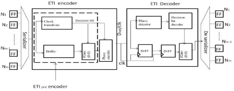
3. PROPOSED ARCHITECTURE
The overall architecture of the ETI scheme is usually shown in Fig We add the ETIpre block. The ETIpre will not offer the decision bit data so it cannot always be decoded inside the receiver. The ETIpre encoder is shown by the dashed box in the ETI encoder. The TIC counts the transitions in the data word then uses this information to do coding. The transition indication piece is added to every single data word to reveal whether there is a great inversion or not. The ETI architecture mainly provides the four sections
Serialization ETI encoder ETI decoder Deserialization
Each serial link features m input bit streams that are multiplexed simply by a serializer, followed simply by the ETI encoding. The encoded stream is sent through the serial link and followed by the ETI decoding and a deserializer.
[image:3.595.94.490.549.703.2]
© 2016, IRJET | Impact Factor value: 4.45 | ISO 9001:2008 Certified Journal
| Page 1365
3.1 Serialization
Serial connection has many advantages above multi bit parallel connection in respects of signal skew, crosstalk, area cost, and wiring congestion. This kind of converts the parallel -line bus into serial links, which reduces the no.of physical bus lines, for the same bus area, this reduction in the number of bus lines causes a bigger interconnect width and pitch (area). For performing almost eight bit serialization 3 levels of selection lines to be needed. Each bit is definitely selected by using a selection line.
3.2 ETI Encoder
The embedded transition inversion scheme encoder block performs the encoding depending up on decision bit the decision bit can be determined by the check transition block. The ETI encoder block uses the buffer for storing the intermediate results.
The ETI encoder section performs the encoding by using three blocks.
Check transition
B2 inversion
Phase encoding
3.2.1 Check Transition Block
The check transition block is employed to find the number of the transitions. The check transition block counts the length of the data word (WL) and generates an high signal at the first bit the data word. This kind of signal is employed to reset to zero the adder and the D-flip-flop (D-FF). The D-FF stores the previous bit that is employed to XOR with the current bit for transition checking. The adder block calculates the number of transition in an data word and sets the decision bit to high when the Nt > =Nth. For the check transition section we are considering the 8
bit data and clock signal as inputs. By using clock signal the input data length will be calculate and then calculate the number of transitions.
3.2.2 B2 Inversion
A transition is defined as a bit changing absolutely from zero to one or from one to zero. For example, the bit stream “01110101” has 5 transition while “10110001” has 3 transitions. When the number of transitions Nt in a data word exceeds the threshold Nth, the bits in the data word should be encoded. Otherwise, the data word remains the same.
be1 = b1
3.2.3 Phase Encoding
The phase generator is used to generate phase difference between the encoded data and clock.
3.3 ETI Decoder
ETI decoder contains the blocks as same as ETI encoder and alexander phase detector and the deserialization block for reconstruction of data.
The decision bit is used in the 2nd bit inversion technique for the decoding. The decoding operator in the 2nd bit inversion technique is the same as that in the encoder.
The inversion decoding operation for the decoded output bd1bd2 is bd1 = be1
© 2016, IRJET | Impact Factor value: 4.45 | ISO 9001:2008 Certified Journal
| Page 1366
3.4 Deserialization
The deserialization is a cambio procedure of the serialization. Here we are used the serial data simply as input to the deserializer then we have parallel data as the final output result. Here the clock signal is divided into 1 / 2 at each level to get deserialization of data.
4. SIMULATION RESULTS
VHDL is commonly used to write text models that describe a logic signal. Such an auto dvd and blu-ray unit is processed simply by a synthesis program, just if it is area of the logic design. A simulation program is employed to test out the logic design applying simulation models to symbolize the logic circuits that interface for the design. This kind of collection of simulation models is commonly called a test bench. Here I am discussing the individual blocks simulation results and their coding descriptions.
A. Serialization
Intended for performing 8 bit serialization 3 levels of selection lines are needed. Every single bit is selected simply by using a selection line.
Fig-2: Imulation Result for Serialization
Pertaining to the parallel to serial section we are used the 8 bit data and clock signal as inputs. By utilizing selection line the input data will certainly be serialized. The final result of serial data is proven as op in the above simulation result.
B. Check Transition Block
For the check transition section we are considered the 8 bit data and clock signal as inputs. By utilizing clock signal the input data size will be calculate and then calculate the number of transitions. The result data db is displays decision bit.
Fig-3: Simulation Result for Check Transition Block
For the check transition block assess the every 2 bit for locating the number of transitions and review to the WL indicator block o/p to choose the decision bit.
C. B2 Inversion
The key porpoise for inversion code is always to reduce the number of transitions.
© 2016, IRJET | Impact Factor value: 4.45 | ISO 9001:2008 Certified Journal
| Page 1367
For the inversion coding block we are considering thealmost eight bit serialized data, decision bit and clock signal as inputs. This block inverts the every second bit depending upon decision bit. The output op shows the 2nd bit inverted data.
D.Phase Encoding
Generally the phase encoding section consists of 3 paths first course non inverted data zero phase difference is supplied between clock and the encoded data. Second course invertsed data plus the third path special data expression for these two paths phase difference is made between clock and the encoded data.
Fig-5: Simulation Result for phase encoder
For the phase encoding block all of us are taken the almost 8 bit serialized data, decision bit and clock signals as inputs. This block provides the phase difference between the clock as well as the data if the data is inverted, else simply no need of phase coding. The output txop displays the encoded data.
E. Alexander Phase Detector
For the alexander period detector section we are considering the 8 bit data and clock signal as inputs. By using clock signal the input data the decision bit can be determined to create the input signal.
Fig-6: Simulation Result for Alexander phase detector
To get the alexander phase detector block we could taken the 8 bit encoded serialized data, decision bit and clock signal as input. This block detects the phase difference between the clock and the data if the phase early on or delay. The result S5S6 and S6S7 reveals the phase difference.
ETI CODING SCHEME FOR 8 BIT DATA
For the ETI block out we are taken the 8 bit serialized data, decision bit and clock signal as inputs. This kind of block reduces the entire number of transitions for serial data. The output tx op is the encoder section output and op is usually the decoder section output.
Fig-7: Simulation Result for ETI coding scheme for 8 bit data
© 2016, IRJET | Impact Factor value: 4.45 | ISO 9001:2008 Certified Journal
| Page 1368
Fig-8: Simulation Results for ETI coding scheme for 16 bitof WL=8
For the ETI block we are considering the 16 bit serialized data, decision bits (db1, db2) and clock sign as inputs. This block out reduces the total number of transitions for serial data. The output txop may be the encoder section outcome and op is the decoder section output (original data).
Advantages:
They have low latency.
It need low hardware over area head.
It has the good thing about utilizing low ability consumption.
Applications:
Computers: System with keypad, mouse.
Communications: Zigbee , Bluetooth.
Biomedical: CRO with ECG.5. CONCLUSIONS
In this project we implemented a great ETI scheme which eliminates the extra bit utilized in the TIC schame and reduces power consumption. This scheme uses the phase difference between the clock and data to reduce the switching activity factor of the serial link. The proposed ETI system achieves greater power decrease compared to
the existing ETI scheme using sequential element. However, larger band width is needed in the ETI coding scheme anticipated to phase shift. The last bit has 1 / 2 the pulse width of the other bits in order that interconnect has twice the bandwidth. It signifies that the serial link needs to run a higher frequency. The higher clock frequency causes problems such as buffering, clock synchronization and design complexity. The different way should be to wait a great extra bit to check on the transition information but that would lower the general bit rate.
6. FUTURE SCOPE
In future there is a scope for achieving greater
power reduction and reduse in transition than the existing ETI scheme by operating each and every device. This can also be implemented on system Verilog where simulation is faster than the Verilog HDL .This seems to greater purpose and advantageous in the upcoming future.
REFERENCES
[1]. Ching. Te chiu,Wen-chih Huang,chih-Hsing Lin ,Wei-chih Lai and Ying-Fag Tsao: “Embedded Transition Inversion with Low Switching Activity for Serial Links” ;IEEE trans on vlsi systems ,vol 21 No 10 ,oct 2013 pp1797–1810.
© 2016, IRJET | Impact Factor value: 4.45 | ISO 9001:2008 Certified Journal
| Page 1369
BIOGRAPHIES
K.Ayyanna completed his Master`s Degree in Telematics & Signal Processing from National Institute of Technology Rourkela and presently working as an Assistant Professor in Brindavan Institute of Technology & Science, Kurnool A.P and permanent member of ISTE .
C.Vishnu vardhan Reddy pursuing Bachelor`s Degree in Electronics & Communication Engineering from Brindavan
Institute of Tech. & Science, Kurnool A.P and member
of ISTE .
A.Ashok pursuing Bachelor`s Degree in Electronics &
Communication Engineering from Brindavan Institute of Tech. & Science, Kurnool A.P.
C.Theja pursuing Bachelor`s Degree in Electronics & Communication Engineering from Brindavan Institute of Tech. & Science, Kurnool A.P.