Journal of Chemical and Pharmaceutical Research, 2014, 6(4):359-364
Research Article
CODEN(USA) : JCPRC5
ISSN : 0975-7384
The study of chaos encryption algorithm for wireless sensor
networks based on the reconfigure technology of FPGA
Kong De-peng
1, Zhu Jun-da
1, He Ting
2and Zhou Yi-fei
11The Center of Technology & Education Development Research, Zhejiang University of Technology, Hangzhou
Zhejiang Province, China
2Hangzhou Nanjiang Internet of Things Technology Co., Ltd. Hangzhou Zhejiang Province, China
_____________________________________________________________________________________________
ABSTRACT
The factors restricting the development of wireless sensor networks (WSNs) included its cost, power consumption and safety. The Field Programmable Gate Array (FPGA) had many advantages with high processing speed, high frequency, low power consumption, rich IP nucleus and microprocessor. It was suitable for WSNs’ node power management and information logic control of acquisition module, storage units and transportation systems. At the same time,FPGA logic resources also used for design the system safety module. The typical chaotic system had high classic white noise and good cryptographic properties, which suited for application in WSNs’ system Security design with the advantages of simple structures and high intensity of security. Given nodes design and the chaotic encryption scheme in this paper based on FPGA Reconfigure technology.
Key words:Wireless Sensor Networks (WSNs); Chaotic encryption; FPGA; Reconfigure
_____________________________________________________________________________________________
INTRODUCTION
Internet of things technology caused the third revolution of the information revolution, mutual communication was spreading from human to objects each other. As wireless sensor networks (WSNs) had a short distance communication and low-cost advantages, it provided a support for networking technology and engineering systems protection [1]. WSNs combined some technologies with information processing, wireless communications, embedded, sensor and so on. which was some variable nodes, owned some abilities of mixed address, quickly self-configuration , high -density building and multi-hop network system, and could realize perception, collection and monitor with deal with all kinds of information , and also had low prices and features on-demand features [2] .It had broad application prospects in many fields, such as defense, energy, ecology, transportation and agricultural. Especially for real-time information remotely monitored that was large-scale, remote or hazardous environmental conditions [3].Therefore, all the countries people in the world focused on the key technologies in this field. But WSNs’ Life Time restricted by the energy consumption, storage capacity, operating speed, computing power, communication reliability, the node security, random arrangement, demand randomness [4]. In recent years, technical and academic experts devoted to reducing energy consumption, improving processing speed [5-6] and increasing security aspects research[ 7].
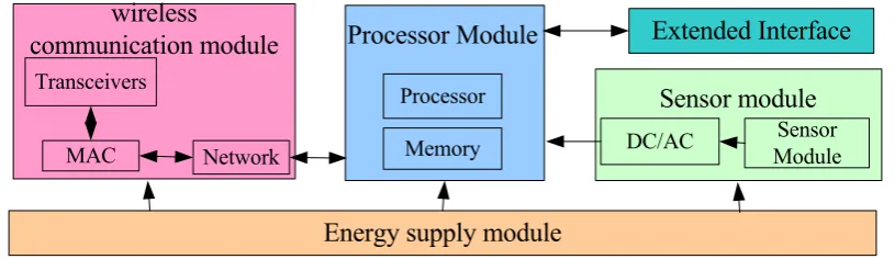
2.FPGA and WSNs’ node design
multi-hop router protocol [8]. Sensor node often have different internal parts included data acquisition unit, processing unit, transmission unit and power management unit. Where, The data acquisition unit in charged of collecting the information and data conversion, the data processing unit controlled the processing operation of the entire node routing protocol and synchronization position, the task of power management unit was energy conservation and distribution, the data transmission unit had responsible for wireless communication with other nodes, exchanged control messages and received collected data, shown as Fig.1. There were a lot of node controllers from different companies, so designed by the different solution methods. But they could be classified by country as follow: Fist, some a series of node systems design funded by the national project design American. Mote node was the first generation series, whose processor designed by Atmel technology and used TinyOS operating system. The second generation node systems were Wec and Mica model, and so on. Other series included Mica2, Mica2Dot and Telos with different core chips. For example, GNOMES series made by Rice University with tiny sensor, making of a Texas Instruments (TI) of MSP430F149, using Bluetooth communication module or 900MHz radio to communicate and the interface using RS232 to achieve communicate with each other. Secondly, some node systems invented by EYES of European research team, which used a Texas Instruments MSP430F149 as the microcontroller, made use of an 8M of EEPROM chip to store programs and data. ESB node system also used the MSP430 MCU of IT company as microcontrollers and used RFM TR1001 as wireless communication blocks. Finally, Gain node system was the first self-developed WSN nodes by Institute of Computing Technology Chinese Academy of Science. Used AVR instruction and radio frequency integrated processor module supports ZigBee protocol. Taken together, these products tend to be integrated processor module in the wireless communication module, some node systems also integrated communication protocols, such as wireless sensor network using microcontroller or DSP chip [9],the external sensor and 2.4GHz wireless transceiver module composed of micro-node[10]. Compared with the microcontroller and DSP, FPGA devices was a single integrated software-defined radio (SDR) signal processor, by the soft-core as the center, it had enough resources to satisfy the need of base station and the functions of node digital IF and baseband. At the same time, the power consumption was less than 0.5watt about 32 NiosII processor of Altera. The preparation of the corresponding procedures and custom hardware logic could control some field data collection of node WSNs, storage and transmission. So the scheme not only could to facilitate the design of online modifications with the interface circuitry integrated on an FPGA, but also could greatly shorten the development cycle of a wireless acquisition node devices [11] .
Energy supply module
wireless
communication module
Transceivers
Network MAC
Processor Module
Processor
Memory
Sensor module
DC/AC Sensor Module
[image:2.595.103.511.408.526.2]Extended Interface
Fig 1. WSNs node hardware system diagram
3. Chaotic module and FPGA Implement
Kong [12]designed a new chaos system, according to the rule of conducive to mask the chaos and generated chaotic attractor[13] , the module equation as follow:
x ax by
y cx dxz ey
z
fxy gx hz
(1)
the parameter of
a b c d e f g h
, , , , , , ,
were Constant, Where the parameters existed25.4,
66.3,
39.21,
1,
rate, when the parameter
t
,each small volume Contained the line rail of system could shrink to zero at an exponential rate, which meant that the system had a dynamic behavior and converges to a final attractor. we used [t, x] = solver ('f', ts, x0, options) and plotted the function to draw, shown as Fig.2 (a), which was one-dimensionaloutput in the time domain waveforms about
x y z
, ,
. At the same time Fig.2 (b) shownx y z
- -
chaotic attractor.0 0 .5 1 1 .5 2 2 .5 3 3 .5 4 4 .5 5 -4 0
-2 0 0 2 0 4 0 6 0 8 0
-4 0 -2 0 0 2 0
4 0 6 0 8 0 -5 0
0 5 00 2 0 4 0 6 0 8 0
(a)
x y z
, ,
Time-domain waveform (b) x-y-z chaotic attractorFig2. chaotic attractor (a) Three-dimensional map (b)x-y-z chaotic attractor
As could be seen from the chart that the three-dimensional chaotic system had more complex chaotic dynamics and unpredictable from its one-dimensional chaotic sequence. This module had three variable parameters and seven constant parameters could be used as seed production chaotic sequence, so this system’s key seed space was greater than the one-dimensional or two-dimensional chaotic system. We could have a encryption processing with a combination of one or more variables, and the design or application was more flexible and convenient than other encryption means. We known this chaotic system usually generated analogy signals, but the chip of FPGA only handled digital or discrete signals. So the system equation must be discrete processing. There were three methods to resolve with Euler algorithm, improved Euler algorithm and Runge-Kutta method, and they had their own advantages and disadvantages. The method of Runge-Kutta algorithm was beast among them, but required a lot of hardware resources with real time computing, in order to improve the speed of operation and save hardware resources, usually used Euler algorithm for discrete processing. However, floating point digital signal processing was the general basic operation, the current FPGA hardware did not provide the appropriate floating point capabilities, only had integer arithmetic capability, it must be discrete processing when used FPGA chip to form chaotic sequences by chaotic systems. Equation (1) discrete form as followed:
(
1) (1
)
(
1)
(1
)
(
1)
(1
)
x n
a T x n
b Ty n
y n
c Tx n
d Tx n z n
e T y n
z n
f Tx n y n
g Tx n
h T z n
( )
( )
( )
( ) ( )
( )
( ) ( )
( )
( )
(3)
The system chosen EP2C35F67C6 model of Altera as the target chip to design WSNs’ node and used VHDL RTL
level language way for description (3),where
a
25.4,
b
66.3,
c
39.21,
d
1,
=1,
f
e
0.9,
g
3,
h
4
,
T
1 10
3this equation could produce chaotic sequence. We designed aTab1. Each state of the Iterative algorithm in the state machine
Status Each status to complete algorithm S0 The initial value x(0)、y(0)、z(0)
S1 X(1)=1.0254x(0),y(1)=0.99991y(0),z(1)=x(0)y(0) S2 X(2)=0.0663y(0),y(2)=-0.0001x(0),z(2)
cut z(0) S3 X(3)=x(1)+x(2),y(3)
cut y(2),z(3)=0.0001z(0) S4 X(4)
cut x(3),y(4)=0.0001y(3),z(4)=0.9996z(0) S5 X(5)=x(4),y(5)=0.9999y(0),z(5)=z(3)+z(4) S6 X(6)=x(5),y(6)=y(1)+y(4)-y(5),z(6)
cut z(5) S7 X(7)=x(6),y(7)
cut y(6),z(7)=z(6)S8 X(0)=x(7),y(0)=y(7),z(0)=z(7)
In order to achieve the design goal, we generated some of the raw data. Such as designed a 16-bit counter, XOR calculator to calculate the resulting data as raw data and 16-bit chaotic signals, get the encrypted data. In the decryption process, we would produce the chaotic signal under the same original conditions [16]. FPGA top-level file schematic of encryption module shown in fig3. The function of int_div model was divide signal, decreased the high-frequency clock signal for FPGA internal design. jiami module function was generated raw data, chaotic signals, and then carried out the encryption process. Gout was one of the original data, Mout was chaotic signals, Lout was signal output of encrypted. These functions would be packaged and generated IP core modules for the use of WSNs’ nodes encryption.
Fig3. FPGA top-level file encryption module chart
4. System Synthesize Based on SOPC
Fig4. WSNs node SOPC achieve schematic
5. Experimental Results and Analysis
5.1 Modelsim Waveform simulation verification
Using SOPC technology to design WSNs’ node system, not only reached the purpose of peripheral logic circuit integrated in a chip,but also realized a hardware encryption / decryption. In order to verify its correctness and availability, we used the simulation tools of Modelsim6.0 to test its validation. For example, there was a plaintext to be encrypted, the test as follow: First, a file of encryption module using VHDL Test Bench tool plaintext to be encrypted and the encryption key sequence. It was defined as the input file, the ciphertext data looked as the output file, and finally called model simulation tool to generate the ciphertext data file while a waveform diagram. Encryption key was 8 shown as in Fig.5, it could be seen from the output waveform, the output ciphertext plaintext output after a one clock cycle obtained. For example, t = 425.378ns, input plaintext Ox76 (01110110), after a delay of a clock, t = 425.376 moment, the output of the corresponding ciphertext 0x83 (10000011).
Fig5. File encryption simulation waveforms
5. 2 An image encryption verification
The transmission function of WSNs nodes included not only data but also the videos or pictures quickly, in order to verify the encryption and decryption of the picture effect, we had to observe the effect of encryption through a grayscale image 256 x 256 on the SOPC node. As shown in Fig.6, the left picture was the original case of the suoqi.JPG, and then entered key and the intermediate iteration encrypted, the image become the middle sample.Then had a decryption and given a right key,the picture restored to its original appearance. This case shown the use of WSN nodes SOPC technology chip programming design and communication encryption and decryption was feasible.
O r ig in a l _ p ic t u r e E n - p ic t u r e D e - p ic t u r e
Fig6. Graphic before and after encryption and decryption
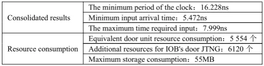
5.3 Consumption Analysis of Resource
By analysis of this system, the software of QuartusII8.0 speeded up to 84.6MHz, every 16 clock cycles could get encryption / decryption a result of 128bit, the equivalent operation rate was 676.8Mb / s, Under the conditions of without changing the algorithm, the design of hardware security was confidentiality,high efficiency, saving energy.
The process of resource consumption of the algorithm made quantitative statistical results were shown in
Table 2. The results of resource consumption statistics in chip integrated
CONCLUSION
It was a convenient method based on-chip programming techniques and rapid reconfiguration technology to design the wireless sensor network node design by NiosII platform. The wireless sensor network node of using SOPC technology could carry out collection, processing, encryption and transmission functions. This way not only improved the system design efficiency, but also conduced to innovative research and development of intellectual
property rights. while, according to different WSNs node with their level of security requirements, we could use
different chaotic systems to form an iterative sequence IP core in FPGA corresponding for node system onfidentiality scheme.
Acknowledgement
The work was Funded by National Science and Technology Support Project (2012BAI34B03), (2012BAI34B02 );National Natural Science Foundation of China(61372087); Ministry of Education, Humanities and Social Science Planning Project(13YJAZH043); Educational Science Planning Project of Zhejiang Province ( 2014SCG040)
REFERENCES
[1]Han-Chiang Chen, Y.-M.Telecommun Syst, Syst,2013(352):2325–2333.
[2]Jesús Lázaro,Journal of Systems Architecture,2011(57) :206–213.
[3]Pan Julong.Research on Some Kev Security Issues for Wireless Sensor Networks.Hangzhou:Zhejiang
University,2011.
[4]Zhu Zheng-jian,TAN Qing-ping,ZHU Pei-dong.Computer Engineering & Science,2008,30(4):101-105.
[5]Xu Xing,WANG Wei-xing,YUE Xue-jun.Science Technology and Engineering,2010,10(6):4005-4008.
[6]Shahabeddin Geravand , Mahmood Ahmadi ,Computer Networks,2013(57) :4047-4064.
[7]Xueying Zhang ,H. M. Heys , Cheng Li.Mobile Netw Appl,2013(18):222–234.
[8]Duc Minh Pham, Syed Mahfuzul Aziz.Computer Networks,2013(57) :2949-2960.
[9]Ding Jian,HU Yu-xi,LI Yun,PAN Jiao.International Electronic Elements,2008(8):37-40.
[10]Meng Qinghao.Chinese Journal Of Sensors And Actuators.2013(4):582-589.
[11]Zhang Guoyi et.Computer Measurement & Control,2012,20(1):243-249.
[12]Kong De-peng.Research and Exploration in Laboratory,2013(10):59-64.
[13]Liu Jian-dong.Journal on Communications,2010(5):51-59.
[14]Zang Bo et.Modern Electronics Technique,2009,294(7):11-14.
[15]Shi Lan-jie et.Open Journal of Circuits and Systems,2013, 2, 39-44.
[16]Li Jia.Computer Engineering,2009,35(9):169-173.
Consolidated results
The minimum period of the clock:16.228ns Minimum input arrival time:5.472ns The maximum time required input:7.999ns
Resource consumption