Modelling and Analysis of EMI Generated of
Power IGBT Modules
Carmine Abbate
1,*, Roberto Di Folco
21DIEI, University of Cassino and Southern Lazio, Via G. di Biasio, Italy 2A.P.F.F Cassino Viale Bonomi n 2, 03043Cassino (FR), Italy
Copyright © 2015 Horizon Research Publishing All rights reserved.
Abstract
Commutations of power IGBT modules used in power converters cause high voltage and current gradients in the collector waveforms, which can generate and irradiate very high electromagnetic noise levels. An innovative experimental - simulative method is presented, which is able to predict irradiated noise levels during converter operation: such method allows power electronics designer to have a proper and simple method to predict spectrum and amplitude of irradiated noise during converter operation, in order to ensure a direct compliance with the enforce normative. The irradiated noise is generated by high frequency conducted current flowing in IGBT module and in the converter. Frequency and amplitude of the internal oscillating currents are simulated by means of a suitable IGBT module model proposed in the past and now optimized for irradiation simulation. The irradiated field during converter operation can be calculated by means of a preliminary static measure executed in anechoic chamber, where the diagram of irradiation of the system is measured at different frequencies, connecting IGBT gate to a radiofrequency generator. Presented results are precise within 3dB limit.Keywords
EMI in IGBT Modules, IGBT Interference, EMI Analysis, EMI Modelling1. Introduction
Achievement of electromagnetic compatibility among the internal components of the converter and between the system and the external environment is a very important and critical task. The introduction of the IGBT (Insulated Gate Bipolar Transistor) module in power electronic converters favoured the reduction of energy losses and the improvement of performances in terms of converter’s weight and switching frequency. These performance enhancements have been possible thanks to the large devices current and voltage ratings and to the reduction of their switching times, but they are accompanied by the strong increase of dv/dt and di/dt that can raise relevant problems of electromagnetic compatibility (EMC) [1]. In effects, power semiconductor devices may
oscillate with stray elements of the circuit [2] thus generating high level of conducted and irradiated electromagnetic noise that could interfere with standard radio frequency apparatuses or with electronic equipment installed in the surroundings of the converter.
The common approach to EMC problems in power converters is to verify the compliance with the normative of the apparatus under investigation, operated in the real field. In case EMC limits are not satisfied, semi-empirical methods to reduce emissions/susceptivity are applied. Results are generally sub-optimal. A more systematical approach would be possible if the designer had a procedure to predict both generated noise frequencies and related level, in effects to predict the irradiated noise interferences during the normal converter operation. The solution to such problem is awkward as electro-mechanical device characteristics and electromagnetic structure properties are coupled and have to be considered. Several studies on the topic have been presented but they are focused on the device behaviour [2, 3, 4] only, either on the electromagnetic structure irradiative properties [5, 6]. More several papers focused on IGBT device modelling and parameters extraction [2, 7] and proposed different radio frequency models.
The present paper proposes an original experimental/simulative procedure which is able to predict the main irradiated noise spectral components and its levels during converter operations. The origin of irradiated noise can be attributed to internal conducted oscillating current that flows in the IGBT and system. In order to obtain these oscillation currents, an appropriate IGBT model proposed in the past [2] has been used. In this paper a novel experimental procedure has been proposed in order to obtain a relationship between internal current distribution and irradiated electromagnetic field.
An exhaustive experimental and numerical simulation analysis is reported in the following.
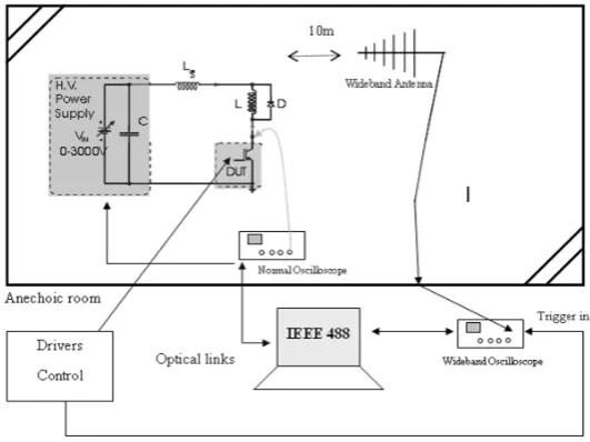
2. Experimental Set Up
normal operation. The global irradiated interference is measured by a selective and settable receiver whose centre band is shifted over the whole investigation band. This method is used in certification tests, aimed at investigating compliance to normative and requires strong efforts to be applicable to high power converters, as high power sources and cooling systems are involved, which are generally not available in the anechoic chamber. Moreover, such method returns an overall evaluation, but it does not allow to separate and analyse the noise components, as related to the IGBT’s commutation. The power device’s main role in the noise generation phenomena is, in this way, not isolated. The method adopted in this paper was proposed in [2] and it requires only a single-shot test on the power inverter so avoiding large power dissipations. The required energy during the commutation is supplied by a DC capacitor charged before the test. The noise irradiated during the turn-on or turn-off switching operations is received by means of a standard wideband antenna positioned at 10m away from and measured with a wideband oscilloscope, external to the room and suitably synchronised with the inverter control circuit.
In such way, noise spectral features are analysed in the frequency domain and the correlation between the time domain waveforms and the frequency spectrum can be straightforwardly studied. The electric schematic of the test set-up is reported in Figure 1: a single inverter phase-leg based on 3300V-1200A IGBT modules is tested in the anechoic room. Particular attention was paid to the connections between the power and control parts for which optical links were used in order to reduce the interference between the radiated noise and the measurement apparatus. All the measured signals are acquired with an external PC connected to the instrumentation by the IEEE488 port.
3. The Adopted IGBT Radio Frequency
Model
The first step to predict the converter irradiated
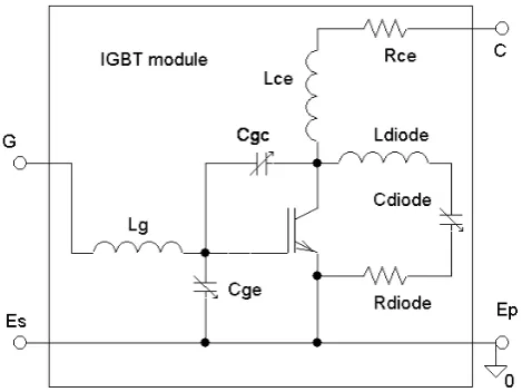
electromagnetic noise is to simulate the origin of irradiation that can be attributed to internal conducted currents. For this goal in this paper we use an IGBT module model proposed in the past and detailed in [2], that is based on physical and electrical internal IGBT characteristics. In short, generated radio frequency noise during device commutations can be attributed to resonant interaction between internal stray inductances and capacitances. We can underline that the model in [2] is not able to predict the level of irradiated noise, but only the main oscillating internal components. For reader’s convenience, the schematic of the model is reported in the Figure 2, where both IGBT and freewheeling diode, physically enclosed in the same case, are taken into account.
We can individuate the following lumped parameters:
gate-emitter equivalent capacitance (Cge), whose
value is variable with the applied gate voltage;
collector-gate capacitance (Cgc), whose value is
variable directly with the collector voltage;
internal diode depletion capacitance (Cdiode), whose
value depends again on the collector voltage;
gate stray inductance (Lg), related to the gate internal
connections;
stray collector (Lc) and emitter (Le) inductances; stray collector-emitter resistance (Rce) related to the
power connections;
internal diode stray inductance and resistance (Ldiode,
Rdiode) related to respective connections.
[image:2.595.169.435.545.744.2]Choice of model components and parameters is fully discussed in [2, 4]. In particular, all the stray capacitor values have been directly measured and the value of the stray inductances have been extracted from the component datasheet. The simple model is able to describe the main spectral components of internal conducted IGBT and diode currents. Stimulus for oscillation can be attributed to the voltage variation during commutation and this was demonstrated in. A similar model has been used recently in [5] in order to predict the conducted noise, but also in this case the irradiated noise cannot be calculated.
Figure 2. Simple IGBT model for the radio-frequency oscillating noise components
4. Simulation of the Conducted Internal
Currents
As a first step, the IGBT and diode model has been used for calculating the internal conducted oscillating current. Moreover in the next sections a relationship between the current, origin of the electromagnetic field, and the irradiated noise will be found by introducing an original experimental-simulative approach.
With reference to the source of the noise, during first commutation part, the low side IGBT is the main responsible of generated noise; instead, in the second commutation phase the freewheeling diode plays the main role. This behaviour was demonstrated thanks to an appropriate time – frequency evolution noise analysis and it has been explained in [4].
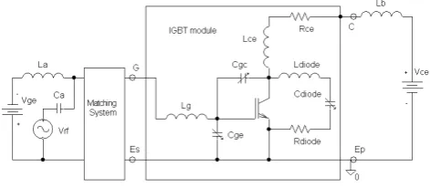
Figure 3. The equivalent circuit of the phase leg accounting the noise generation
4.1. Converter Equivalent Circuit
Internal IGBT and diode noise currents during operation can be calculated using the complete electric schematic of the inverter phase leg reported in Figure 3.
Model includes: the IGBT and diode model for the low side IGBT (Lsg, Cge, Cgc, Ldiode1, Rdiode1 and Danti1), the diode part of this model for the high side IGBT module which acts as a free wheeling diode (Ldiode, Rdiode and Danti), the equivalent stray inductance of the external circuit (Ls), the bus-bar stray inductance (Lce) and capacitance (Cbus). Moreover the circuit shows also the Cdc dc supply capacitance and the respective stray Ldc inductance. The parameters used for the elements of the above model were extracted by means of the procedure presented in [2]. Their values are summarized in Table 1.
An original approach has been used to account for the active device and diode effects. In detail, due to the importance of the dv/dt evolution as stimulus for noise generation, the IGBT and freewheeling diode devices have been modelled by means of equivalent current and voltage PWL generators. The corresponding look-up tables have been directly extracted by experimental waveforms. This approach is a simple and accurate way to model a complex phenomenon as reverse recovery of a power diode, overcoming limitations of available circuital equivalent models.
PSPICE simulation allows evaluation of the currents that flow through the IGBT and diode stray elements [8]. Such currents are the origin of the radiated noise. It is worthy underlining that such internal currents cannot be easily experimentally measured, as their circulation path is all internal to IGBT module, so not easily accessible for measurements, without modifying high-frequency system evolution.
4.2. Simulation Results
The simulation analysis was performed during the IGBT turn-on operation with the objective to compare to experimental results.
Noise analysis showed that mainly current in Miller capacitance Cgc and current in Danti capacitance are mainly responsible of the emission [2]. The twos act in different commutation phases.
Figure 4 reports main IGBT experimental waveforms measured during the turn-on phase. Testing conditions are: power supply Vcc=1500V, load current Ic=300A, Rgon=0.31Ω. These conditions induce very high gradients, both on collector voltage (3.7kV/µs) and current (4kA/µs).
Noise waveform received at the antenna during the commutation is reported in the lower part of Figure 5. In particular, noise appears as collector voltage fall begins. (see figures 4 and 5)
signal noise, that will be calculated in the following. Due to linearity of Maxwell’s equations [10], it is correct to consider a proportionality factor between the oscillating current and the irradiated noise. Experimental waveforms in Figure 5 show that in the first phase of commutation, the noise frequency is about 35 MHz, and in the second turn on phase it is reduced at about 21MHz. Moreover also a low frequency component at about 3.6MHz is present.
[image:4.595.63.294.365.504.2]Figure 4.Waveforms across the IGBT and freewheeling diode
Figure 5.Received noise signal, simulated noise signal Simulation results show very similar characteristics, both in amplitude and frequency range. Regarding the low frequency components, we can remember that it is related to others external converter stray parameters that are not considered in this model [11].
5. Radiation Properties of the Converter
System
The second step to predict the amplitude of the spectral components irradiated during the converter operation, is the determination of factor of proportionality between the internal conducted currents and the electric field which is responsible for the voltage measured at the antenna.
This factor can be obtained by analytical solution of the Maxwell equations [6] or by experimental measurements. The analytical methods impose to know the physical distribution of the sources, hence internal geometrical details
of the IGBT modules which are not generally available. For this reason in this paper an original experimental procedure is proposed in order to correlate the conducted internal currents with the irradiated electric field in different angular direction. In particular the diagram of irradiation of the whole converter is measured by injecting a current waveform at different frequency in the IGBT module. In this way, thanks to the linearity of the involved equations, we can individuate a relationship between internal current and received voltage. In other words, the IGBT module in the converter is treated as a transmitting antenna where the supply currents are the oscillating internal currents.
5.1. Measure of Converter Irradiation Diagram
[image:4.595.315.551.392.495.2]Whereas the IGBT module is the main responsible for generated noise current, the IGBTs of the converter system have been connected to a radio frequency source through the gate terminal. In this way, the apparatus is assimilated to a transmitting antenna and the overall signal include both the effects of current sources flowing in IGBT chip and the ones related to diode ones. The schematic of the supply system is reported in Figure 6. An appropriate impedance matching system is arranged between the Vrf (50Ω) radio frequency source and the IGBT gate in order to maximize the power delivery to the system.
Figure 6. Experimental circuit used to supply the radio frequency signal at the IGBT module
Moreover power device gate and collector are dc polarized in order to have the correct values of the internal stray capacitances. In particular, the DC collector voltage has been set to the nominal value (Vce=1500V). Moreover the gate voltage was set equal to Vge=-15V in order to maintain the IGBT module in its interdiction region.
system can be roughly modelled as a short dipole, so that directivity is low [10] and irradiation factor increases with the frequency. The irradiation isotropy is very important as it simplifies our analysis. In fact it will be enough to calculate the emitted noise for one spatial direction, in order to achieve a complete characterization.
Figure 7. Diagram of irradiation of the whole converter, feed from a radio frequency current
5.2. Input Impedance of IGBT Module
(A)
(B)
Figure 8. IGBT input resistance (A) and reactance (B)
The factor of proportionality between the source current and received voltage noise must consider the real current which is transferred to the IGBT device. For this reason, device input impedance was measured by means of a network analyzer in order to design the input matching network of Figure 6. In particular the input resistance is reported in Figure 8-a, and the related reactance in the Figure. 8-b, in the range 20MHz – 1GHz. In our range of interest (20-50MHz) both input resistance and reactance are very low (about 1Ω). In particular in Figure 8-b, we can recognize a series resonance at about 30MHz. (the input reactance is reduced to zero).
6. Evaluation of the Noise Emission
After the measurement of the irradiation diagram associated to the converter and of the effective current transferred to the devices, we can individuate the relation between source current and received voltage.As an example, from the small signal analysis at 30MHz input frequency signal, we have measured the input current I0=9.1mA, and the output voltage at the antenna V0=30.3dBµV/m. Then the proportionality factor α can be defined [10]: α=V0/I0=3.6mV/A.
After such small-signal high-frequency measurements, the emitted noise during the normal converter operation can be predicted, scaling the internal currents that flow in the internal stray elements. Of course this procedure estimates field at the same distance, which was set in measurements between the converter and measurement antenna in the case of small signal, and commutation operation. Of course, best practical choice is to make all the characterizations at 10 m distance in order to estimate the predictions of the radiated noise at the reference distance set by railway standard EN 50121.
The consistency of the proposed procedure has been verified with reference to previous simulation. In Figure 9 solid line shows the experimental received noise spectrum whereas dotted line represents the predicted spectrum in the range 10MHz, 100MHz. In particular the experimental FFT waveform shows the main harmonic components at about 36MHz, 25MHz. The simulated procedure allow to predict very well the high frequency components at about 36MHz and 25MHz.
Amplitudes are similar within 3dB factor. In fact if we consider the 36MHz component, we individuate an amplitude value of 1.6mV for the experimental data and 2.2mV regarding the simulated value.
[image:5.595.57.295.378.726.2](B)
Figure 9. Experimental and predicted radiated noise spectra
7. Conclusions
Table 1. The values of the parameters used in the phase leg equivalent circuit
Quantity Value
Cgc 7nF @Vce=0
Cge 600 nF @ Vge=-15 V
Cdiode 53 nF @ Vce=0 V
Cdiode1 53 nF @ Vce=0 V
Lce 10 nH
Lg 20 nH
Ldiode 4.5 nH
Ldiode1 4.5 nH
Rdiode 0.1 Ω
Ls 80nH
Cbus 700pF
Cdc 2800µF
Ldc 50nH
R 33kΩ
An innovative procedure that allows us to predict the frequency and amplitude of the main irradiated noise components has been presented.
The method is based on a circuit simulation which uses a radio frequency IGBT model proposed in the past and which allows to calculate the internal oscillating current that are the origin of noise irradiation.
The correlation between the internal currents and the received voltage noise, can be evaluated by means of an original experimental procedure that is based on the linearity of Maxwell’s equations and uses a preliminary measure
executed on the system that is considered as a transmitter antenna. The prevision error associated to the procedure is lower than 3dB.
The proposed method can be used by converter designer as a synthesis method for achieving given EMI goals (“Design to EMI”).
REFERENCES
[1] R. Redl: “Power electronics and electromagnetic compatibility”, Power Electronics Specialists Conference, 1996, PESC '96 Record., 27th Annual IEEE Volume 1, 23-27 June 1996 pp.15 - 21 vol.1.
[2] G. Busatto, C. Abbate, F. Iannuzzo, L. Fratelli, B. Cascone, G. Giannini: “EMI Characterization of high power IGBT modules For Traction Application” Power Electronics Specialists Conference, 2005, PESC 05, Record 36th, pp. 2180-2186, Recife - Brazil.
[3] P.R. Palmer, J. C. Joyce: “Circuit analysis of active mode parasitic oscillations in IGBT modules”, IEE Proceedings Circuit Devices, pp 85-91, April 2003.
[4] C. Abbate, G. Busatto, L. Fratelli, F. Iannuzzo: “EMI Analysis in High power Converters for Traction Application” EPE 2005, 11-14 September 2005, Dresden, Germany. [5] Dong Zhang, Liang Kong, Xuhui Wen: “A novel simple
IGBT model for power electronic systemsEMI simulation, ITEC Asia-Pacific, pp. 1-5, 2014, DOI: 10.1109/ITEC-AP.2014.6941036.
[6] R. Thomas, F. Li, C. Garrett: “Prediction of Radiated EMI from High Frequency Power Converters”, Power Electronics and Variable Speed Drives, pp.80-85, 18-19 September 2000. [7] W.G. Garlick: “EMC analysis for power electronic equipment”, Predicting and Assuring EMC in the Power Electronics Arena, IEE Colloquium on 15 Feb 1994 pp. 5/1 - 5/7.
[8] C. Martin, J. L. Schanen, R. Pasterczyk: “Inside a Power Module”, Industry Applications Conference, 39th IAS Annual Meeting. Conference Record of the 2004 IEEE, pp. 1519-1525, October 2004.
[9] C.L.Ma, P.O. Lauritzen, J Sigg: “Modeling of power diodes with the lumped-charge modeling technique”, Power Electronics, IEEE Transactions on Vol 12, May 1997 pp. 398 – 405.