http://dx.doi.org/10.4236/cs.2015.610023
How to cite this paper: Kushwaha, A.K. and Paul, S.K. (2015) Current Mode Universal Filter Using Single Current Controlled Differential Difference Current Conveyor Transconductance Amplifier. Circuits and Systems, 6, 224-236.
http://dx.doi.org/10.4236/cs.2015.610023
Current Mode Universal Filter Using Single
Current Controlled Differential Difference
Current Conveyor Transconductance
Amplifier
Ajay Kumar Kushwaha, Sajal K. Paul*
Department of Electronics Engineering, Indian School of Mines, Dhanbad, India Email: [email protected], *[email protected]
Received 26 August 2015; accepted 27 October 2015; published 30 October 2015
Copyright © 2015 by authors and Scientific Research Publishing Inc.
This work is licensed under the Creative Commons Attribution International License (CC BY). http://creativecommons.org/licenses/by/4.0/
Abstract
This research paper contains a new electronically tunable current-mode biquadratic universal filter using a new active building block; current controlled differential difference current con-veyor transconductance amplifier (CCDDCCTA). The proposed filter provides the following im-portant and desirable features: (i) One can use only one CCDDCCTA and two capacitors; (ii) One can get low pass (LP), band pass (BP), high pass (HP), notch (NF) and all pass (AP) current res-ponses from the same configuration without any alteration; (iii) Passive components are grounded, which ease the integrated circuit implementation; (iv) Responses are electronically tunable; and (v) Sensitivity is low. Moreover, the non-ideality analysis shows that the parasitic passive components can be compensated for the proposed circuit. The functionality of the design is verified through SPICE simulations using 0.25 µm CMOS TSMC technology process parameters. Simulation result agrees well with the theoretical analysis.
Keywords
Current Mode Analog Filter, Universal Filter, Current Controlled Differential Difference Current Conveyor Transconductance Amplifier (CCDDCCTA), Monte-Carlo Analysis
1. Introduction
Universal biquadratic filters are those which provide all standard filter functions (low pass (LP), band pass (BP),
high pass (HP), notch (NF) and all pass (AP)), without modifying the circuit topology. The advancement in the field of microelectronics presents current mode active building blocks for design of fast and high performance analog signal processing circuits and systems [1]. The current mode active blocks may process signals in voltage as well as current mode. A number of current mode filters using various analog building blocks (ABB) are available in literature under the classification of multi-input multi-output (MIMO) [2]-[5], single-input multi- output (SIMO) [6]-[11] and multi-input single-output (MISO) [12]-[24]. In addition, a range of current conveyor blocks with inbuilt transconductance amplifier (TA) in monolithic chip, such as current conveyor transconductance amplifier (CCTA) [25], current difference transconductance amplifier (CDTA) [26], current controlled current conveyor transconductance amplifier (CCCCTA) [27], differential voltage current conveyor transconductance amplifier (DVCCTA) [19], differential difference current conveyor transconductance amplifier (DDCCTA) [4], differential voltage current controlled conveyor transconductance amplifier (DVCCCTA) [28] and current con-trolled differential difference current conveyor transconductance amplifier (CCDDCCTA) [29], have emerged in last few years. Among these, CCDDCCTA is a recently introduced ABB. It is basically composed of current controlled differential difference current conveyor (CCDDCC) [30] followed by a transconductance amplifier (TA) block. It has high input impedance terminals for voltage and high output impedance terminals for currents. It can process both differential and floating inputs. It inherits all the good properties of CCDDCC, CCCCTA and DDCCTA along with electronic tuning of transconductance, which is found to be useful in design of various circuits with lesser number of resistors and integrated circuit implementation.
The study of MISO universal filters [13]-[24] based on current mode ABB reveals that these circuits suffer one or more of the following weakness:
(a) Use of two or more ABBs [13]-[16] [18] [20]-[24];
(b) Excessive use of the passive components [15]-[17][19][21]; (c) No grounded passive components [15][16];
(d) Requirement of four or more input current signal to get all the responses [15]-[18]; (e) Requirement of gain of input signal such as 2Iin or 3Iin [13]-[15] [20][23][24]; (f) Lack of electronic tunability [15][16];
(g) Non-orthogonality of pole frequency and quality factor [13]-[15] [20]-[22][24].
A new current mode universal filter with a reduced number of passive components has been presented. The proposed filter is a multi-input single-output (MISO) and uses two grounded capacitors and one CCDDCCTA only. The proposed current mode filter circuit can realize high pass (HP), low pass (LP), band pass (BP), notch and all pass (AP) filter responses by selecting appropriate input current without alteration of the topology. It can easily be cascaded, as its output is current and impedance is high. All the features of the proposed filter can be electronically adjusted by biasing currents of the CCDDCCTA. Moreover, the high-Q filter may easily be achieved by using the bias currents of CCDDCCTA. A comparative study of the available active elements based on current mode filters is also presented. PSPICE simulation results verify the theoretical analysis.
2. Circuit Description
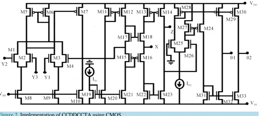
[image:2.595.193.439.571.713.2]The symbol of CCDDCCTA and its implementation using CMOS are shown inFigure 1and Figure 2 respec-tively.
Figure 2.Implementation of CCDDCCTA using CMOS.
The port relationships of the CCDDCCTA can be represented by the following matrix:
1 1
2 2
3 3
01 01
02 02
0 0 0 0 0 0 0
0 0 0 0 0 0 0
0 0 0 0 0 0 0
1 1 1 0 0 0
0 0 0 1 0 0 0
0 0 0 0 0 0
0 0 0 0 0 0
Y Y
Y Y
Y Y
X X X
Z Z mo mo I V I V I V
V R I
I V
I g V
I g V
= − − − (1)
where, the intrinsic resistance
( )
Rx at X terminal defined as16 18 1 x m m R g g =
+ (2)
where,
16 1
16 2
m ox B
W
g C I
L
µ
=
(3)
18 1
18 2
m ox B
W
g C I
L
µ
=
(4)
Similarly, the transconductance
( )
gmo from Z terminal to O terminal may be expressed as2 25,26 2
mo ox B
W
g C I
L
µ
=
(5)
It may be noted that both
( )
RX and( )
gmo can be electronically varied by bias currents IB1 and IB2 of CCDDCCTA respectively.The proposed current mode (CM) filter is shown in Figure 3which utilizes two grounded capacitors and one CCDDCCTA only. The routine analysis of circuit gives the output current at single node as:
(
2)
1 1 2 1 2 1 3
2
1 2 1
mo in x mo in x mo in
out
x mo
g I sC R g I s C C R sC g I I
s C C R sC g
− − + + +
=
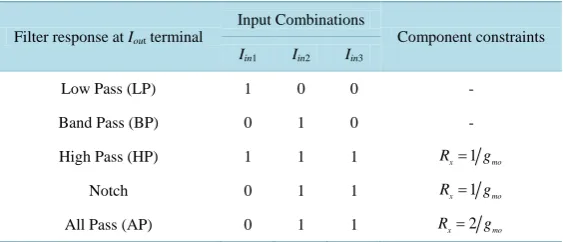
The inspection of Equation (6) reveals that the circuit of Figure 3 will function as a universal filter depending upon combination of inputs (Iin1, Iin2 and Iin3) applied at three terminals. The output response (Iout) for different combinations of inputs are shown in Table 1. It reveals that no component constraint is required for LP and BP response; however for HP, notch and AP responses a simple component matching is required. The circuit is suitable for cascading to another circuit having low input impedance for current input.
The filter parameters, namely natural angular frequency ( )ω0 , bandwidth (BW) and quality factor ( )Q0 are
obtained respectively as
1 2 0 1 2 mo x g C C R
ω =
, 0 0 2 1 x BW
Q C R
ω
= = , and
1 2 2 0
1
mo x
g R C Q
C
=
(7)
It reveals in Table 1 and (7) that for LP and BP responses ω0 and Q0 can be varied with IB2 without dis-turbing ω0 Q0 . The variation of ω0 without disturbing Q0 may be achieved by simultaneously varying IB1 and IB2, such that the product g Rmo x remains constant and the quotient gmo Rx varies and vice-versa.
Simi-larly for HP and notch responses ω0 can be varied independent of Q0 by keeping the product g Rmo x unity
and varying the quotient gmo Rx using IB1 and IB2. It may also be shown from (7) that high value of quality factor
( )
Q0 can be obtained from the low spread of capacitance (C1 and C2) values [31]. If the ratio of C1 andC2 are chosen as g Rmo x =C C2 1, then the spread of components comes out to be Q0 . This feature of the proposed filter allows the realization of high Q0 with low spread of C1 and C2 in comparison to topologies where the spread is Q0 or
2 0
Q .
The sensitivity of a parameter Y to variation of element X may be defined as
d d Y X X Y S Y X
= (8)
The sensitivity analysis of the proposed circuits for various parameters is evaluated as
0 1
2
mo
g
Sω = , 0 0 0
1 2
1 2
x
C C R
[image:4.595.198.453.379.551.2]Sω =Sω =Sω = − ,
Figure 3.Proposed current mode universal filter.
Table 1. The Iin1, Iin2 and Iin3 values selection for each filter function re-sponse.
Filter response at Iout terminal
Input Combinations
Component constraints
Iin1 Iin2 Iin3
Low Pass (LP) 1 0 0 -
Band Pass (BP) 0 1 0 -
High Pass (HP) 1 1 1 Rx=1gmo
Notch 0 1 1 Rx=1gmo
[image:4.595.173.455.597.718.2]2 x 1
BW BW
C R
S =S = − (9)
0 0 0
2
1 2
mo x
Q Q Q
g C R
S =S =S = , 0 1
1 2
Q C
S = − .
It reveals that the sensitivity is low and less then unity in magnitude.
3. Non-Idealities Analysis
The performance of the proposed current mode filter might be deviated from the ideal response due to non- idealities of CCDDCCTA. The first non-ideality comes due to the internal current (α) and voltage (β) transfer of CCDDCCTA and hence modified port relationships with current and voltage transfer non-ideality can be ex-pressed in matrix form as
1 1
2 2
3 3
1 2 3
01 01
02 02
0 0 0 0 0 0 0
0 0 0 0 0 0 0
0 0 0 0 0 0 0
0 0 0
0 0 0 0 0 0
0 0 0 0 0 0
0 0 0 0 0 0
Y Y
Y Y
Y Y
X X X
Z Z mo mo I V I V I V
V R I
I V
I g V
I g V
β β β
α γ γ = − − − (10)
where, voltage tracking error coefficient β1, β2 and β3 are from Y1, Y2 and Y3 terminals to X terminal re-spectively. The current tracking error coefficient α is from X to Z terminal. The current gain coefficient γ is from Z terminal to O terminal. Considering these tracking coefficient, modified output current of the circuit is obtained as:
(
2)
3 1 1 2 1 2 1 2 3 3
2
1 2 1 2 3
mo in x mo in x mo in
out
x mo
g I sC R g I s C C R sC g I
I
s C C R sC g
αβ γ γ αβ αβ γ
αβ αβ γ
− − + + +
=
+ + (11)
The filter parameters can be expressed as
3 0 1 2 mo x g
C C R
αβ γ
ω = , 0 2
0 2 x BW
Q C R
ω αβ
= = , 3 2
0 2
2 1
mo x
g R C Q
C
β γ αβ
= . (12)
It is noticed that the non-idealities affect the parameters of the filter. The sensitivity analysis of ω0, Q0 and
BW results as follows:
0 0 0 0
3
1 2
mo
g
Sω =Sβω =Sαω =Sγω = , 0 0 0
1 2
1 2
x
C C R
Sω =Sω =Sω = − , 0 0
1 2 0
Sβω =Sωβ = ,
2 1
BW BW
Sβ =Sα = ,
2 x 1
BW BW
C R
S =S = − ,
1 3 1 0
mo
BW BW BW BW
g C
S =Sβ =Sβ =S = , (13)
0 0 0 0 0
2 3
1 2
mo x
Q Q Q Q Q
g C R
S =S =S =Sβ =Sγ = , 0 10 20
1 2
Q Q
Q C
Sα =S =Sβ = − , 10 0 Q
Sβ = .
It reveals that with non-ideality; the sensitivity is still low and magnitude is within unity.
The second non-ideality comes due to the parasites of CCDDCCTA comprising of capacitances and resis-tances connected in parallel at Z, O and Y terminals. The effect of these parasites is very much dependent on the circuit topology. The current mode universal filter with non-ideality is shown in Figure 4. The modified capa-citances are C1′ =C1 CY3 C01 and G2′ =C2 CY2 CZ and modified resistances/conductances are
(
)
1 1 Y2 Z
G′ = R R and G2′ =1
(
RY3 R01)
. Here, CY2, CY3, CZ and CO1 are the parasitic capacitances at Y2, Y3,capacitances C1 and C2 lesser by (CY3 + CO1) and (CY2 + CZ) respectively from their calculated values. The effect
of parasitic conductances may also be made insignificant if operating frequency and value of C1 and C2 are cho-sen in such a way that
sC
1
G
1′
andsC
2
G
2′
.4. Simulation Result and Discussion
The current mode universal filter as proposed in Figure 3 is simulated with PSPICE. The 0.25 µm CMOS TSMC technology process parameters are used for simulation. The aspect ratio of various transistors is stated in
Table 2. The supply voltages of ±1.25 V and VBB = −0.8 V are used. To design the filter for a pole frequency of
0
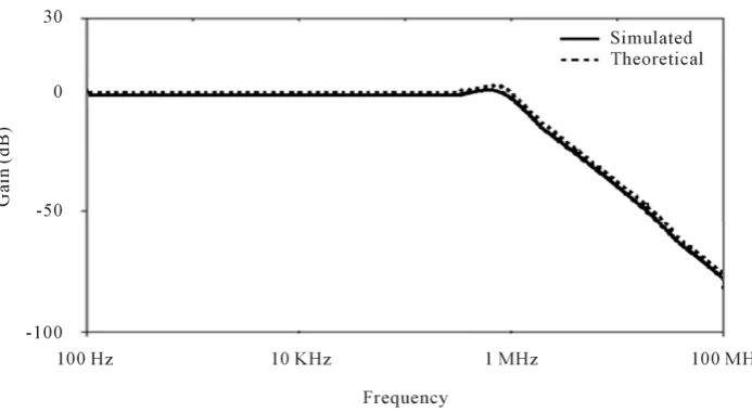
f = 1.28 MHz and quality factor Q0 = 1, the component values are taken as C1 = C2 = 100 pF and bias cur-rent as IB1 = 25 µA and IB2 = 200 µA. The input for each filter realization is selected as per Table 1. Figures 5-8 shows the simulated and theoretical low pass, high pass, band pass and notch responses respectively. The value of IB1 is set as 12.5 µA and IB2 = 200 µA for the realization of all pass responses as shown inFigure 9.
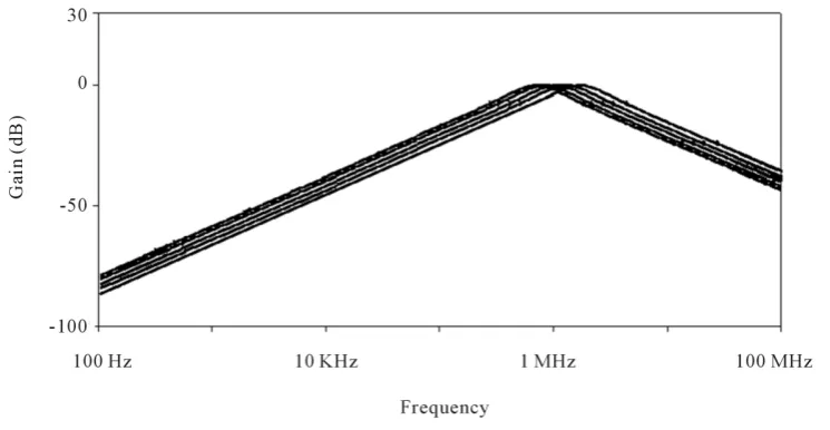
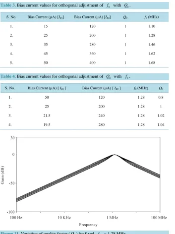
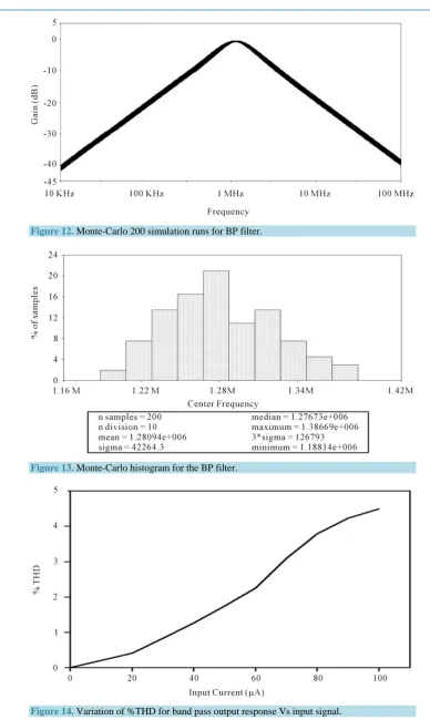
To test the orthogonal variation of f0 with Q0, a band pass filter is chosen. The variation of f0 with Q0
= 1 is shown in Figure 10 for different value of bias currents (IB2 = 8 IB1) as given inTable 3. Similarly Figure
11shows orthogonal adjustment of Q0 with f0 = 1.28 MHz for different value of IB1 and IB2 as mentioned in
Table 4.
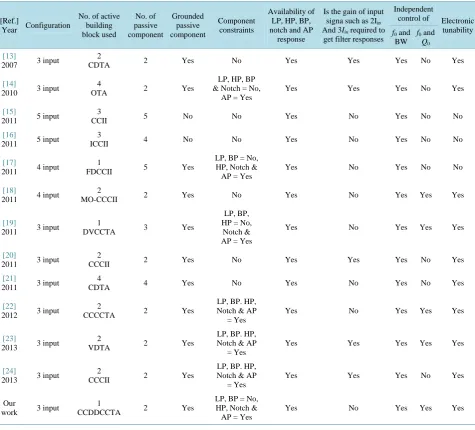
It is well known that a little tolerance of the value of the various components occurs during manufacturing and even afterword resulting in deviation of various parameters of filters such as central frequency, quality fac-tor and bandwidth from its designed values. The collection of statistical data due to tolerance of passive compo-nents is obtained using Monte-Carlo analysis for band pass filter. As an example, for a 100 pF ± 5% capacitor, the actual measured capacitor value to be somewhere between 95 pF and 105 pF. Monte-Carlo runs to cover as
Figure 4. Current mode universal filter with non-ideality.
Table 2. Aspect ratio of various transistors.
Transistors Aspect Ratio W(µm)/L(µm)
M1-M4 1.0/0.25
M5-M6, M11-M14, M17, M25-M30 5.0/0.25
M7 12.5/0.25
M8-M10, M19-M23, M31-M33 3.0/0.25
M15 8.0/0.25
M16 9.0/0.25
M18 4.5/0.25
Figure 5.Simulated and theoretical response for low pass filter.
Figure 6.Simulated and theoretical response for high pass filter.
[image:7.595.134.494.509.706.2]Figure 8. Simulated and theoretical response for notch filter.
Figure 9. Simulated and theoretical gain and phase response for all pass filter.
[image:8.595.129.502.508.701.2]Table 3. Bias current values for orthogonal adjustment of f0 with Q0.
S. No. Bias Current (µA) [IB1] Bias Current (µA) [IB2] Q0 f0 (MHz)
1. 15 120 1 1.10
2. 25 200 1 1.28
3. 35 280 1 1.46
4. 45 360 1 1.62
5. 50 400 1 1.68
Table 4. Bias current values for orthogonal adjustment of Q0 with f0.
S. No. Bias Current (µA) [ IB1 ] Bias Current (µA) [ IB2 ] f0 (MHz) Q0
1. 50 120 1.28 0.8
2. 25 200 1.28 1
3. 21.5 240 1.28 1.02
[image:9.595.144.498.81.554.2]4. 19.5 280 1.28 1.04
Figure 11.Variation of quality factor (Q0) for fixed f0 = 1.28 MHz.
many possible values of the component within their tolerance limits. It is performed by taking 5% Gaussian deviation of C1 and C2 values for 200 simulation runs for a pole frequency of 1.28 MHz. The result of Monte- Carlo simulation is shown inFigure 12and corresponding histogram inFigure 13. As per statistical results as shown in Figure 13, the minimum and maximum frequency obtained are 1.18 MHz and 1.38 MHz respectively and standard deviation is 42.2 KHz. It reveals that the proposed filter exhibits a reasonable sensitivity perfor-mance. The quality of the output response may be judged with the help of percentage total harmonic distortion (%THD). The %THD of the output response for band pass filter with respect to the input is shown inFigure 14. It is found that the %THD is well within the tolerance range of 5%.
Comparative study of different available implementation of current mode MISO universal filters is given in
Figure 12. Monte-Carlo 200 simulation runs for BP filter.
Figure 13.Monte-Carlo histogram for the BP filter.
[image:10.595.139.488.343.696.2]Table 5. Comparative study of the available active element based current mode MISO universal filter.
[Ref.]
Year Configuration
No. of active building block used No. of passive component Grounded passive component Component constraints Availability of LP, HP, BP, notch and AP
response
Is the gain of input signa such as 2Iin
And 3Iin required to
get filter responses
Independent
control of Electronic tunability
f0 and
BW
f0 and Q0
[13]
2007 3 input
2
CDTA 2 Yes No Yes Yes Yes No Yes
[14]
2010 3 input
4
OTA 2 Yes
LP, HP, BP & Notch = No,
AP = Yes
Yes Yes Yes No Yes
[15]
2011 5 input
3
CCII 5 No No Yes No Yes No No
[16]
2011 5 input
3
ICCII 4 No No Yes No Yes No No
[17]
2011 4 input
1
FDCCII 5 Yes
LP, BP = No, HP, Notch & AP = Yes
Yes No Yes No No
[18]
2011 4 input
2
MO-CCCII 2 Yes No Yes No Yes Yes Yes
[19]
2011 3 input
1
DVCCTA 3 Yes
LP, BP, HP = No,
Notch & AP = Yes
Yes No Yes Yes Yes
[20]
2011 3 input
2
CCCII 2 Yes No Yes Yes Yes No Yes
[21]
2011 3 input
4
CDTA 4 Yes No Yes No Yes No Yes
[22]
2012 3 input
2
CCCCTA 2 Yes
LP, BP. HP, Notch & AP
= Yes
Yes No Yes Yes Yes
[23]
2013 3 input
2
VDTA 2 Yes
LP, BP. HP, Notch & AP
= Yes
Yes Yes Yes Yes Yes
[24]
2013 3 input
2
CCCII 2 Yes
LP, BP. HP, Notch & AP
= Yes
Yes Yes Yes No Yes
Our
work 3 input
1
CCDDCCTA 2 Yes
LP, BP = No, HP, Notch & AP = Yes
Yes No Yes Yes Yes
5. Conclusion
Current mode universal filter using current controlled differential difference current conveyor transconductance amplifier (CCDDCCTA) has been presented that uses two grounded capacitors and one CCDDCCTA only. It can realize high pass, low pass, band pass, notch and all pass responses from the same topology. The filter pa-rameter can be electronically adjustable by bias currents IB1 and IB2. Table 5shows the comparative study of the available current mode building block based MISO filters. PSPICE simulation results authenticate the theoreti-cal results.
References
[1] Ferri, G. and Guerrini, N.C. (2000) Low-Voltage Low-Power CMOS Current Conveyors. Kluwer Academic Publishers, Dordrecht, Netherlands.
[3] Siripruchyanun, M. and Jaikla, W. (2008) Electronically Controllable Current Mode Universal Biquad Filter Using Single DO-CCCDTA. Circuits, Systems, andSignalProcessing, 27, 113-122.
http://dx.doi.org/10.1007/s00034-008-9014-2
[4] Pandey, N. and Paul, S.K. (2011) Differential Difference Current Conveyor Transconductance Amplifier (DDCCTA): A New Analog Building Block for Signal Processing. JournalofElectricalandComputerEngineering, 2011, Article ID: 361384.
[5] Chen, H.P. (2012) Tunable Versatile Current Mode Universal Filter Based on Plus-Type DVCCs. International
Jour-nalofElectronicsandCommunications, 66, 332-339. http://dx.doi.org/10.1016/j.aeue.2011.08.010
[6] Prasad, D., Bhaskar, D.R. and Singh, A.K. (2009) Universal Current Mode Biquad Filter Using Dual Output Current Differencing Transconductance Amplifier. InternationalJournalofElectronicsandCommunications, 63, 497-501. http://dx.doi.org/10.1016/j.aeue.2008.02.012
[7] Mangkalakeeree, S., Duangmalai, D. and Siripruchyanun, M. (2009) Current Mode KHN Filter Using Single CCCCTA.
TheSeventhPSUEngineeringConference, 21-22 May 2009, Songkla, Thailand, 306-309.
http://www.te.kmutnb.ac.th/~msn/khncctapec7.pdf
[8] Wanga, C., Xua, J., Keskinb, A.Ü., Dua, S. and Zhanga, Q. (2011) A New Current Mode Current Controlled SIMO- Type Universal Filter. InternationalJournalofElectronicsandCommunications, 65, 231-234.
http://dx.doi.org/10.1016/j.aeue.2010.02.010
[9] Tangsrirat, W. (2011) Single Input Three-Output Electronically Tunable Universal Current Mode Filter Using Current Follower Transconductance Amplifiers. InternationalJournalofElectronicsandCommunications, 65, 783-787. http://dx.doi.org/10.1016/j.aeue.2011.01.002
[10] Pandey, N., Nand, D. and Khan, Z. (2013) Single Input Four-Output Current Mode Filter Using Operational Floating Current Conveyor. ActiveandPassiveElectronicComponents, 2013, Article ID: 318560.
[11] Prasad, D., Bhaskar, D.R. and Srivastava, M. (2013) Universal Current Mode Biquad Filter Using a VDTA. Circuits
andSystems, 4, 29-33. http://dx.doi.org/10.4236/cs.2013.41006
[12] Siripruchyanun, M. and Jaikla, W. (2007) Current Controlled Current Conveyor Transconductance Amplifier (CCCCTA): A Building Block for Analog Signal Processing. In: Proceedings of the International Symposium on
CommunicationsandInformationTechnologies, IEEE Computer Society Press, Sydney, 209-211.
http://dx.doi.org/10.1109/iscit.2007.4392014
[13] Tangsrirat, W., Dumawipata, T. and Surakampontorn, W. (2007) Multiple Input Single Output Current Mode Multi-function Filter Using Current Differencing Transconductance Amplifiers. International Journal ofElectronics and
Communication, 61, 209-214. http://dx.doi.org/10.1016/j.aeue.2006.04.004
[14] Lee, C.N. (2010) Multiple Mode OTA-C Universal Biquad Filters. Circuits, Systems&SignalProcessing, 29, 263-274. http://dx.doi.org/10.1007/s00034-009-9145-0
[15] Horng, J.W. (2011) High Output Impedance Current-Mode Universal Biquadratic Filters with Five Inputs Using Multi- Output CCIIS. MicroelectronicsJournal, 62, 693-700. http://dx.doi.org/10.1016/j.mejo.2011.02.007
[16] Horng, J.W. (2011) Current-Mode Universal Biquadratic Filter with Five Inputs and One Output Using Tree ICCIIs.
IndianJournalofPure&AppliedPhysics, 49, 214-217.
http://nopr.niscair.res.in/bitstream/123456789/11155/1/IJPAP%2049(3)%20214-217.pdf
[17] Senani, R., Abdalla, K.K. and Bhaskar, D.R. (2011) A State Variable Method for the Realization of Universal Current- Mode Biquads. CircuitsandSystems, 2, 286-292. http://dx.doi.org/10.4236/cs.2011.24040
[18] Channumsin, O., Pukkalanun, T. and Tangsrirat, W. (2011) Universal Current-Mode Biquad with Minimum Compo-nents. Proceedings of the InternationalMultiConferenceofEngineeringandComputerScientists, Hong Kong, 16-18 March 2011, 1012-1015. http://www.iaeng.org/publication/IMECS2011/IMECS2011_pp1012-1015.pdf
[19] Pandey, N. and Paul, S.K. (2011) VM and CM Universal Filters Based On Single DVCCTA. ActiveandPassive
Elec-tronicComponents, 2011, Article ID: 929507. http://dx.doi.org/10.1155/2011/929507
[20] Kumngern, M. (2011) Multiple-Input Single-Output Current-Mode Universal Filter Using Translinear Current Con-veyors. JournalofElectricalandElectronicsEngineeringResearch, 3, 162-170.
http://dx.doi.org/10.5897/jeeer11.023
[21] Tangsrirat, W. and Pukkalanun, T. (2011) Structural Generation of Two Integrator Loop Filters Using CDTA and Grounded Capacitors. InternationalJournalofCircuitTheoryandApplications, 39, 31-45.
http://dx.doi.org/10.1002/cta.616
[22] Jaikla, W., Siripongdee, S. and Suwanjanmiso, P. (2012) MISO Current-Mode Biquad Filter with Independent Control of Pole Frequency and Quality Factor. Radioengineering, 21, 886-891.
[23] Satansup, J., Pukkalanun, T. and Tangsrirat, W. (2013) Electronically Tunable Current-Mode Universal Filter Using VDTAs and Grounded Capacitors. Proceedings oftheInternational Multi Conference ofEngineersand Computer
Scientists, Hong Kong, 13-15 March 2013, 2.
http://www.iaeng.org/publication/IMECS2013/IMECS2013_pp647-650.pdf
[24] Srisakultiew, S., Lawanwisut, S. and Siripruchyanun, M. (2013) A Current-Mode Electronically Controllable Multi-function Biquadratic Filter Using CCCIIs. InternationalJournalofAdvancesinTelecommunications, Electrotechnics,
SignalsandSystems, 2, 45-50. http://dx.doi.org/10.11601/ijates.v2i1.11
[25] Jaikla, W., Silapan, P., Chanapromma, C. and Siripruchyanun, M. (2008) Practical Implementation of CCTA Based on Commercial CCII and OTA. ProceedingsoftheInternationalSymposiumonIntelligentSignalProcessingand
Com-municationSystems, Bangkok, 8-11 December 2008, 1-4. http://dx.doi.org/10.1109/ispacs.2009.4806670
[26] Biolek, D. (2003) CDTA-Building Block for Current-Mode Analog Signal Processing. ProceedingsoftheEuropean
ConferenceonCircuitTheoryandDesign, Cracow, 1-4 September 2003, 397-400.
http://user.unob.cz/biolek/veda/articles/ECCTD03_2.pdf
[27] Siripruchyanun, M. and Jaikla, W. (2008) Current Controlled Current Conveyor Transconductance Amplifier (CCCCTA): A Building Block for Analog Signal Processing. ElectricalEngineering, 90, 443-453.
http://dx.doi.org/10.1007/s00202-007-0095-x
[28] Maiti, S. and Pal, R.R. (2013) Universal Biquadratic Filter Employing Single Differential Voltage Current Controlled Conveyor Transconductance Amplifier. LectureNotesonPhotonicsandOptoelectronics, 1, 56-61.
http://dx.doi.org/10.12720/lnpo.1.2.56-61
[29] Pandey, N., Kumar, P. and Choudhary, J. (2013) Current Controlled Differential Difference Current Conveyor Trans-conductance Amplifier and Its Application as Wave Active Filter, ISRNElectronics, 2013, 1-11.
http://dx.doi.org/10.1155/2013/968749
[30] Prommee, P. and Somdunyakanok, M. (2011) CMOS-Based Current Controlled DDCC and Its Applications to Capa-citance Multiplier and Universal Filter. InternationalJournalofElectronicsandCommunications, 65, 1-8.
http://dx.doi.org/10.1016/j.aeue.2009.12.002
[31] Liu, S.L. (1995) High Input Impedance Filters with Low Component Spread Using Current Feedback Amplifier.