FPGA Implementation of Single Bit Error Correction
using CRC
Pramod S P
Department of ECE, DSCE,VTU,Bangalore,India
Rajagopal A
Department of E&C, DSCE, VTU,Bangalore, INDIA
Akshay S Kotain
Department of E&C, DSCE, VTU,Bangalore, INDIA
ABSTRACT
Transferring data between two points is very essential, also the accuracy of the transferred data is vital for some critical applications, but an error during the transmission of data is very common. The Cyclic Redundancy Check (CRC) method is generally used for error detection and correction. In this paper, we have proposed a new technique for error detection and correction in case of CRC-16, which is hardware optimized and works at relatively higher frequency and speed. In the proposed method, it is possible to detect the exact place of single bit error and correct them using minimum hardware. This method involves no look tables and hence is memory efficient. This paper focuses on effective implementation of this method on FPGA.
Keywords
CRC, Field Programmable Gate Array, Single bit error correction, Parallelism, non-lookup technique.
1.
INTRODUCTION
The Internet is growing rapidly in terms of number of users and amount of bandwidth used. Besides the transmission and switching speeds, the per-packet operations necessary for internet Protocol (IP) packet forwarding are the current limiting factors. As transmission speeds are continually increasing, IP packet processing overheads have become the main bottleneck [5]. The received data may not be same as the transmitted data because of noise and interference, which leads to errors during the process of data transmission and storage. Hence, to achieve better quality data transmission, coding and detection methods are employed. CRC is very simple and efficient method to detect and correct the errors. A Cyclic Redundancy Check (CRC) is a type of function that takes an input data stream of any length, and produces an output value of 32-bit or 24 bit integer. Single bit error correction using look up table technique was presented in [3] and [4]. A CRC can be used as a checksum to detect accidental alteration of data during transmission or storage. A CRC theoretically can correct all single, double and odd bits in error [6]. The process of encoding and decoding are discussed in the following sections.
In this paper, we have introduced a new approach for the error detection and correction using non-look up table technique based on FPGA, in case of CRC. This approach is memory efficient and operates at high frequency. Since most of the methods currently employed are based on look up table technique, they consume more space and also there will be a reduction in speed because of the overhead required in accessing the ROM which stores the look up table. We will then review the Sunil Shukla [1] method that corrects single bit error and also other look up table optimization techniques presented in [2]. We have also discussed a method which makes the algorithm hardware implementable and the results obtained are tabulated.
2.
PRINCIPLE
CRC is one of the most famous and robust error control methods. Its computation resembles a long division operation in which the quotient is discarded and the remainder becomes the result, with the important distinction that the arithmetic used is the carry-less arithmetic of a finite field or Modulo-2 addition. The length of the remainder is always less than or equal to the length of the divisor, which therefore determines how long the result can be.
In this method, the receiver divides the data by generator polynomial and then gets the remainder. The receiver then uses parallelism technique to correct single bit error by a shifter circuit which will be explained in the following sections. This improvised proposed method requires zero memory and minimum hardware.
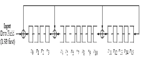
[image:1.595.318.551.479.579.2]Before transmission, the frame produced by CRC encoder consists of check bits cascaded with data bits. These check bits which are redundant are used for error detection and correction at the receiver. For the calculation of checksum bits, a fixed generator polynomial is chosen. The data bits are then divided with the generator polynomial and the resultant remainder is the checksum bits. The division of the data by the generator polynomial is performed using the circuit which is shown in Figure 1.
Fig 1: Polynomial divider.
Initially, all the remainder registers are initialized to zero. Then the data bits are shifted into the circuit with the order such that the LSB of data is entered into the circuit first. Now depending upon the generator polynomial, the data is just shifted right or it is added with the feed- back value. Modulo-2 addition is performed. Once all the data bits are shifted into the registers, the remainder registers indicates the checksum bits. These checksum bits are cascaded with the data bits before the data is transmitted.
The codeword C(x) can be calculated using Equation 1.
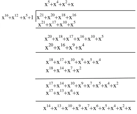
The first part of right hand side of Equation 1 represents the checksum bits. Here ‘n’ represents the frame width and ‘k’ represents the data width. As an example taking n= 24 and k=8 the calculation of checksum bits is shown below.
x
5+x
4+x
2+x
x16+x12 +x5+1
x
21+x
20+x
18+x
16x
21+x
17+x
10+x
5
x
20+x
18+x
17+x
16+x
10+x
5x
20+x
16+x
9+x
4
x
18+x
17+x
10+x
9+x
5+x
4x
18+x
14+x
7+x
2
x
17+x
14+x
10+x
9+x
7+x
5+x
4+x
2x
17+x
13+x
6+x
x
14+x
13+x
10+x
9+x
7+x
6+x
5+x
4+x
2+x
Here:
Data, D(x):00010011
Check bits:00110011011110110
Codeword, C(x):00110011011110110__00010011
Similarly the codeword for CRC-16 can be calculated. The CRC Encoder is designed to generate the codeword in a single clock cycle with high speed and efficiency.
Frame Structure of CRC-16:
Check bits (32 down to 17) Data bits(16 down to 1)
Frame Structure of CRC-8:
Check bits (24 down to 9) Data bits(8 down to 1)
3.
PROPOSED METHOD FOR ERROR
DETECTION AND CORRECTION
In this paper, we will be presenting a unique way of implementing multiple bit error detection and single bit error correction using CRC for a frame width of 24 bits and 32 bits. Let Ftr be the frame transmitted in which the checksum is appended after 16 or 8 bits of data. We can express Ftr as shown in Equation 2.
Ftr = Dtr & Ctr (2)
Where,
& - concatenation operator. Dtr- transmitted 16 or 8 bit data. Ctr - transmitted 16 bit checksum.
At the receiver side, let Fre be the received frame as shown in Equation 3.
Fre = Dre & Cre (3) Where,
Cre indicates received checksum.
Dre represents received data.
Receiver again calculates CRC on the received data. Let Ccal indicates the CRC calculated over Dre at the receiver side. If no error has occurred during transmission then Cre and Ccal are equal. But if some bit(s) are in error, then Cre and Ccal will be in mismatch. In such cases the error needs to be detected and corrected .Hence we need to calculate the syndrome which is given by:
[image:2.595.51.289.129.327.2]Syn=Cre XOR Ccal (4) If the syndrome is calculated as proposed in [9] which uses a circuit similar to the circuit as shown in Figure 1, only with more number of registers, then it requires as many clock cycles as the number of bits in the codeword. But by using equation 4, the syndrome can be calculated in minimum number of clock cycles .This method of syndrome calculation was proposed in [1] and is an efficient one, hence we have adopted it.
Table 1. Possible number of error patterns
This paper uses two standards CRC-16 and CRC-8 for correcting single bit errors. Here we have designed the algorithm to detect more than one error and we will raise a flag indicating retransmission of the frame if there were more than one error.
There are 2 cases in which the single bit error can occur. In the first case, one bit error can occur in the data bits. In the second case, one bit error can be in checksum bits. Hence the total number of possible single bit errors in data for both the standards is shown in Table 1.
For CRC-16 if ‘i’ is the position of the error then for case 1) 1≤ i ≤16 and for case 2) 17≤ i ≤32 . Similarly for CRC-8 only the limits will change.
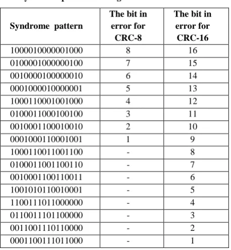
In our proposed method we have used a new technique for detecting errors in both the cases (described in previous paragraph). This method is an outcome of the fact that if an error occurs as in case 2 then the syndrome pattern will have 1’s equal to no. of bits in error. As we know, we only have to correct the error in the data bits, there is no need to correct the error which has occurred in the checksum bits. But we need to detect the errors in the checksum bits. This method of analysis is advantages since it reduces memory requirements by 76% and also we need to worry only about the errors in data, this reduces the load on the computational block of the receiver. The analysis of the two cases mentioned above is explained in detail by using tables. The syndrome pattern for Case 2 for CRC-16 is shown in Table 2. This pattern is similar even for CRC-8. As we can see the pattern consists of only bit with logical level 1. Similarly Table 3 represents the syndrome patterns of the Case 1 for CRC-16 and CRC-8 standards. In [1] only lower 8 bits are used for addressing leading to 256 memory locations. Also, the no. of patterns to be checked in [1] is only 32. Hence the above type of addressing is not applicable. Here we require the entire 16 bits of the syndrome for locating and correcting the data. This results in 65536 memory locations. Considering a ROM with 65536 or 256 memory locations is not so efficient when compared to our
Standard Single Bit Error
CRC-8 24
method of not using any memory block at all. We can analyze the syndrome more effectively without using any memory. The use of ROM [8] also introduces complexity into the design, since we need to constantly read error patterns from it and to take care of correct timing.
Table 2. Syndrome patterns of single bit error in check bits
Syndrome pattern Location of the bit in error (i)
0000000000000001 17
0000000000000010 18
0000000000000100 19
0000000000001000 20
0000000000010000 21
0000000000100000 22
0000000001000000 23
0000000010000000 24
0000000100000000 25
0000001000000000 26
0000010000000000 27
0000100000000000 28
0001000000000000 29
0010000000000000 30
0100000000000000 31
1000000000000000 32
[image:3.595.54.283.152.382.2]To explain the method of correcting single bit error that we have proposed let us consider an example of (7,4) CRC code as in [9]. The syndrome generator circuit for this codeword is shown Figure. 2. This circuit of shift registers is similar to the circuit shown in Figure 1 except that it has only three shift registers corresponding to three check bits in the codeword.
Fig 2: syndrome circuit for (7,4)
Here the generator polynomial used is g(x)=1+x+x3. The received vector Z=1110101 with three check bits and a nibble of data. In this codeword first three MSB bits are check bits which is concatenated with a nibble of data. Here the 3rd MSB or 3rd Check bit is in error. So we need to detect it and correct it. In conventional method the output of the circuit in Figure 2 which is syndrome is used to address a look up table which actually stores the error pattern. This error pattern is then XORed with the CRC frame to get the correct data.
Table 3. Syndrome patterns of single bit error in data bits
Syndrome pattern
The bit in error for
CRC-8
The bit in error for
CRC-16
1000010000001000 8 16
0100001000000100 7 15
0010000100000010 6 14
0001000010000001 5 13
1000110001001000 4 12
0100011000100100 3 11
0010001100010010 2 10
0001000110001001 1 9
1000110011001100 - 8
0100011001100110 - 7
0010001100110011 - 6
1001010110010001 - 5
1100111011000000 - 4
0110011101100000 - 3
0011001110110000 - 2
0001100111011000 - 1
But, in the proposed method the same circuit in Figure 2 is used but more number of clock cycles are required. That is when all the 7 received bits are entered into the syndrome calculator, ‘0’s are now fed into it, from 8th shift onwards as shown Table 4. Each time a ‘0’ is fed into the circuit, the shift register contents are tabulated. This process of feeding ‘0’s continues till the shift register contents read S0 S1 S2 =100. In general for (n-k) shift register, the contents should read S0, S1……. Sn-k-1 = 1 0 0………….0. i.e., 1 followed by (n-k-1) number of 0s. In Table (4), we find that at the 12th shift we get shift register contents as 100. The error is then located and corrected as given below.
Table 4. Contents of shift register in the syndrome calculator
No. of shifts
Input Z(x)
Shift Register Contents
S0 S1 S2
Initialization and LSB of Z(x) enter
first
Shift register contents are cleared
0 0 0
1 1 1 0 0
2 0 0 1 0
3 1 1 0 1
4 0 1 0 0
5 1 1 1 0
6 1 1 1 1
7 1 0 0 1
8 0 1 1 0
9 0 0 1 1
10 0 1 1 1
11 0 1 0 1
[image:3.595.57.278.479.602.2]As we can see from Table (4) after 7th shift we get the syndrome from the circuit in “fig 2”. Since this syndrome is not equal to “000” it indicates an error. Then the procedure is continued as explained earlier until 12th shift when shift register content is “100”. This shift number indicates the position of the error as shown below.
The 5th bit counting from right is in error. Therefore Error pattern is E=0010000 Corrected vector V= Z XOR E
= 1110101 XOR 0010000 V = 1100101
This is the same method employed in correcting single bit error in CRC-8 and CRC-16.
4.
IMPLEMENTATION ON FPGA
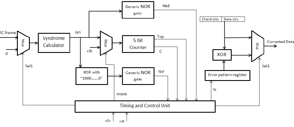
A parallel VLSI architecture of the decoder circuitry is as shown in “Fig.3”. The syndrome calculator generates the vector syndrome from the received frame based on the circuit similar to “fig 1”. This operation requires 32 clock cycles and hence this timing is kept track by a Timing and Control Unit with the help of a 5 bit counter. Then if the syndrome is all zero, it means that the corrected data is same as received data or else if the number of 1’s in the syndrome pattern is equal to 1, it indicates an error in the check bits. Finally, if single bit error is present in data bits which is indicated by the above equations not being satisfied then 0’s are input into the syndrome calculator circuit and after each 0 input the vector syndrome is XORed with the pattern “0000000000000001” and checked whether the result is zero or not. If it is zero then the corrected data is obtained by XORing the received data
with the error pattern register content. If not then the procedure is continued and error pattern register content is shifted towards left by 1 bit. The initial content of error pattern register is “0000000000000001”.
[image:4.595.64.576.535.757.2]Fig 4: state diagram of the control unit
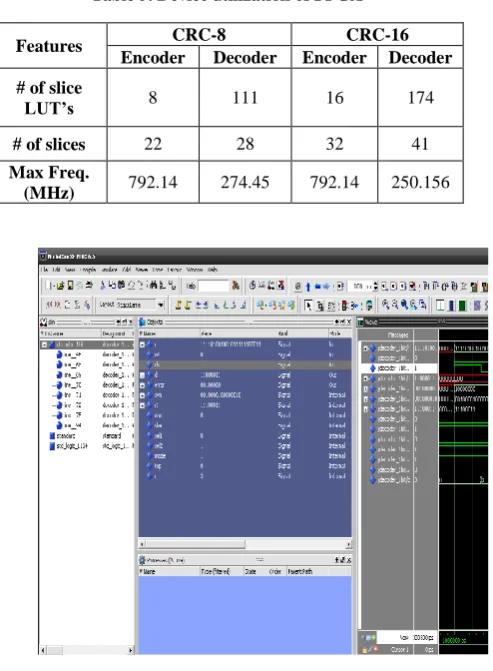
[image:5.595.53.300.349.685.2]The algorithm has been implemented and verified on Xilinx Virtex-5 FPGA device. The code was written in VHDL and synthesized using XST (Xilinx synthesis tool). The device used for implementation is xc5vlx30 with speed grade 3. The results obtained are summarized in Table 5. Simulation is carried out using MODELSIM SE 6.5 and the simulation results are shown in Figure 5.
Table 5. Device utilization of FPGA
Fig 5: Modelsim Simulation
5.
CONCLUSIONS
CRC is the method that can detect the error in transferring data between two points. In this paper a new method based on
CRC has been introduced for single bit error correction. We have implemented on FPGA, for two different standards CRC-8 and CRC-16. We have shown that hardware implementation on FPGA can be effectively used to improve the performance of CRC calculations.
Usually components, like shift registers, XOR and NOR gates are used, so the entire circuit can be easily designed. This approach is efficient both in terms of hardware and speed. The additional hardware required is very simple. This technique works efficiently in case of ASIC design also.
The hardware requirements are tabulated and the algorithm is tested for all possible inputs using a test bench and the algorithm performs as designed.
6. REFERENCES
[1] Shukla S, Bergmann N W. “Single bit error correction implementation in CRC-16 on FPGA” In: IEEE International Conference on Field-programmable Technology. Brisbane,Australia, 2004: 319-322.
[2] PAN Yun, GE Ning, DONG Zaiwang. “CRC Look-up Table Optimization for Single-Bit Error Correction”. In: TSINGHUA SCIENCE AND TECHNOLOGY ISSN 1007-0214 18/19 pp620-623 Volume 12, Number 5, October 2007.
[3] Johnston C A, Chao H J. “The ATM layer chip: An ASIC for BISDN applications”. IEEE Journal on Selected Areas in Communications, 1991, 9(5): 741-750. [4] Peterson, W. W. and Brown, D. T. “Cyclic Codes for
Error Detection “Proceedings of the IRE 49: 228. doi: 10.1109/JRPROC.1961.287814, January 1961.
[5] W.W Peterson, E. J. Weldon. “Cyclic Codes for Error Detection”.Second Edition Published by MIT Press, 1972 ISBN 0262160390,9780262160391.
[6] Norman Matloff. “Cyclic Redundancy Checking”. [7] “Double Bits Error Correction Using CRC Method” by
Shahram Babaie, Ahmad Khadem Zadeh, Seyed Hasan Es-hagi, Nima Jafari Navimipour.IN: Semantics, Knowledge and Grid, 2009. SKG 2009. Fifth International Conference. Oct. 2009, 254 – 257, 11050651.
[8] “FPGA implementation of one and two bit error correction using CRC” by Pramod S P, Akshay S kotain, Rajagopal A in International conference on recent trends in computer science and engineering 2012,ISBN 978-81-9089-807-2.
[9] Digital and analog communication systems, K. Sam Shanmugam, John Wiley, 1996.
[10]Giureppe Campobello, Giuseppe Patane. Marco Russo, ”Parallel CRC Realization”.
[11]T. V. Ramabadran and S. S. Gaitonde. “A tutorial on CRC computations”. IEEE Micro, Vol. 8, No. 4, 1988, pp. 62-75.
[12]T. B. Pei and C. Zukowski “High-speed Parallel CRC Circuits in VLSI” IEEE Tran.on Communications,Vol. 40, April, 1992, pp 635-657
Features CRC-8 CRC-16
Encoder Decoder Encoder Decoder
# of slice
LUT’s 8 111 16 174
# of slices 22 28 32 41
Max Freq.