Tailoring magnetoresistance at the atomic level: An
ab initio
study
Kun Tao and V. S. Stepanyuk
Max-Planck-Institute of Microstructure Physics, D-06120 Halle, Germany
I. Rungger and S. Sanvito
School of Physics and CRANN, Trinity College, Dublin 2, Ireland
(Received 15 September 2011; revised manuscript received 16 December 2011; published 5 January 2012) The possibility of manipulating the tunneling magnetoresistance (TMR) of antiferromagnetic nanostructures is predicted in the framework of ab initio calculations. By the example of a junction composed of an antiferromagnetic dimer and a spin-polarized scanning tunneling microscopy tip we show that the TMR can be tuned and even reversed in sign by lateral and vertical movements of the tip. Moreover, our finite-bias calculations demonstrate that the magnitude and the sign of the TMR can also be tuned by an external voltage. DOI:10.1103/PhysRevB.85.045406 PACS number(s): 75.76.+j, 72.25.−b, 75.30.Et, 85.75.−d
I. INTRODUCTION
When electrons tunnel from one magnetic electrode into another through a barrier, the magnitude of the tunneling current depends on the relative magnetization orientation of the two electrodes, which, in a magnet with uniaxial anisotropy, can be switched between a parallel and an antiparallel configuration with an external magnetic field. In this manner stable low- and high-resistance states can be realized. This is known as the tunneling magnetoresistance (TMR) effect,1–3 the foundation of modern hard-drive read heads and magnetic random access memories. The goal of obtaining a large TMR ratio has focused intensive theoretical4–7and experimental8–10
studies on improving the structural quality of the interfaces in magnetic tunnel junctions so that the tunneling process remains coherent.
Another route for achieving a large TMR ratio is that of scaling down the device’s size below the nanometer level toward single-atom dimensions. If this route is taken, the ability to control and manipulate the spin states of atomic-scale structures will become a crucial challenge. In general the spin state of a single magnetic atom or molecule can be controlled by depositing it on magnetic substrates11–17 or insulator thin
films,18,19 or by making it part of a variable length magnetic chain.20 However, fixing and controlling the spin direction
of atomic-scale structures without an external magnetic field still remains a formidable task. In order to achieve this goal the use of systems with large magnetic anisotropy energy is a natural choice. Transition metal dimers are believed to fall into this category, which makes them promising candidates for magnetic storage owing to their ultra-small size.21,22Most
importantly, it has been proven that their local spin states can be manipulated locally with an external electric field.23
In the present paper, we propose a new method for engineering the conductance and the TMR at the atomic level by a spin-polarized scanning tunneling microscopy (STM) tip. Here we choose a Co-Cr heteronuclear dimer as a model system and focus on the electron transport between the dimer and a Cr tip. Our spin-dependent transmission calculations demonstrate that the amplitude and the sign of the TMR can be tailored by vertical or lateral motion of the STM tip as well as by the applied bias.
II. CALCULATION METHODS
We performed ground-state density functional theory (DFT) calculations using the VASP code24 within the gen-eralized gradient approximation (GGA), with the exchange-correlation functional of Perdew and Wang (PW91).25In order
to describe the ion core electrons, the projector augmented wave (PAW) potentials are used.26 The valence electronic
states are expanded in terms of plane waves with the number restricted by a maximal kinetic-energy cutoff of 400 eV. All parameters in calculations are chosen to converge the total energy to 10−4 eV. The geometries are relaxed until
all the residual forces are smaller than 0.01 eV/A. The˚ transport calculations are performed with theSMEAGOLcode,27
which combines the nonequilibrium Green’s function (NEGF) formalism with DFT as implemented in SIESTA.28 In all the transmission calculations, we used a standard double-ζ
polarized basis for Cu and a triple-ζ basis plus polarization orbitals for thesshell for both Co and Cr. A 2×2 in a plane
k-point grid and a real-space mesh cutoff of 350 Ry are used. The Cu(001) substrate is modeled by a five-layer-thick slab containing 16 atoms in each atomic plane. The tip is modeled as a pyramidal cluster,29constructed from nine Cu atoms and
terminated with a single Cr atom at the tip-apex, which is the same geometry adopted in our previous work.30We have also
checked the stability of our results with the tip geometry and noted very little variations.31
The energy-dependent transmission coefficient,Tσ(E;V), is self-consistently evaluated at the finite biasV and integrated to give the spin current
Iσ(V)= e
h
dETσ(E;V)[fL−fR], (1)
Note that the actual potential drop in the device is calculated self-consistently.
III. RESULTS AND DISCUSSION A. Heteronuclear dimer on metal surface
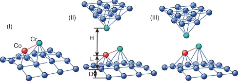
A Co-Cr heteronuclear dimer is placed above the top Cu layer at different sites, such as the top, bridge, and hollow ones on the (001) surface. After full atomic relaxation, the hollow site is calculated to be the most energetically favorable binding position between the adatom and the surface. The total energy of the system in this case is about 1.15 eV lower than that of the bridge site, and even lower than that of the top one. Thus, the Co-Cr dimer is placed with the atoms above two nearest hollow positions. The vertical distance between Co in the dimer and the Cu atoms underneath, LCo−Cu, is 1.54 ˚A,
while it is 1.80 ˚A for Cr,LCr−Cu. The relaxed local geometry is presented in Fig.1(I). The substrate also shows an upward relaxation with a distortionDsubof 0.04 ˚A.
The magnetic order of the dimer is mainly determined by the direct exchange interaction between Co and Cr, and it is characterized by two basic collinear spin alignments, in which the local magnetic moments are either parallel (P configuration) or antiparallel (AP configuration) to each other. The energy difference between two configurations is defined asEex=EP−EAP. We calculateEex= +186 meV, which means that the spins are in a robust AP alignment. Because of the interaction with the supporting substrate or host, the global spin orientation of a nanostructure can be driven into a noncollinear configuration. Thus, we extend our investigations into different noncollinear spin orientations, and we determine the magnetic anisotropy of the system. We find that the ground state is an in-plane (with respect to the Cu surface) collinear AP configuration, and the magnetic moment of the Co (Cr) atom is 1.59μB(3.79μB). As such, the hard axis of the dimer
is out-of-plane, and the total energy in this case is about 1.6 meV higher than that of the in-plane position.
A Cr-terminated tip is positioned right above the Co atom and it is moved toward the dimer as shown in Fig.1. First, the spin orientation of the dimer at different tip-atom distances (HTA) is carefully investigated. In our calculations, the spin
direction of the Cr termination of the tip is fixed to be out-of-plane, while the spin direction of the dimer is rotated.
Co Cr (I)
(II) (III)
H
L
D
[image:2.608.312.559.140.200.2]FIG. 1. (Color online) Setup for our transport calculations. (I) The Co-Cr heteronuclear dimer on the Cu surface. (II) and (III): The full device setup including the Cr-terminated tip and the dimer. These are positioned, respectively, at a large (5 ˚A) and a short (3 ˚A) tip-atom distance. HereH is the tip-atom distance,Lis the vertical distance between atoms of the dimer and the substrate atoms underneath atoms, andDis the distortion of the substrate.
TABLE I. Total energy in meV of the dimer-tip system when the Cr tip is positioned above the Co atom of the dimer at different tip-atom distances ( ˚A) for different spin configurations. Coσ (Crσ) (σ =↑,↓) is the spin orientation of the Co (Cr) atom in the dimer and Tσ is that of the tip. All the energies are measured with respect to the ground-state configuration, which in all cases is Co↓Cr↑T↑. HTA( ˚A) Co↓Cr↑T↑ Co↓Cr↑T↓ Co↑Cr↓T↑ Co↓Cr↓T↑
5 0 5.1 5.1 111.6
4 0 26.3 26.3 131.2
3 0 118.9 118.9 102.7
At large tip-atom distances,HTA=5 ˚A, where the junction
is in the tunneling regime, the easy axis of the dimer is no longer in-plane but rotates out-of-plane. Now the energy of the out-of-plane arrangement is about 3.6 meV lower than that of the in-plane one (the hard-axis is in-plane now). The physics behind this rotation is rooted in the fact that the Cr tip provides a perturbation to the dimer ground state. Thus, the weak indirect interaction between the tip and the dimer along the direction orthogonal to the surface moves the dimer spin orientation out-of-plane. The energy difference between out-of-plane configuration and in-plane one becomes larger as the tip-atom distance is reduced. This increases to 13.5 meV forHTA=4 ˚A, and it jumps to 25 meV forHTA=3 ˚A (contact regime).
We have then calculated the energy of the system at three tip-atom separations for different collinear spin configurations of the Co and the Cr atoms of the dimer and of the Cr tip-apex (T). The results are summarized in TableI.
From the table it can be observed that in all cases the ground state is characterized by a dimer AP configuration and by an AP alignment between the Cr atom of the tip and the Co in the dimer. Therefore, in all our next calculations we fix the spin direction of the Co-Cr dimer in such a way that the spin direction of the Co is perpendicular and points into the substrate while that of the Cr points out of it.
The geometry of the dimer-tip system changes as the tip approaches the surface. At the large tip-atom distanceHTA=
5 ˚A, due to the weak interaction between the tip and the dimer,
LCo−Cu slightly increases to 1.54 ˚A, while LCr−Cu remains 1.80 ˚A. The magnetic moment of the Co (Cr) atom of the dimer is 1.58 (3.78)μB; i.e., it is nearly unchanged as compared to the dimer in the absence of the tip. In this situation the magnetic moment of the Cr atom of the tip is 3.96μB. At the closer tip-atom distance ofHTA=3 ˚A, the atoms in the dimer are pulled upward,LCo−Cu increases to 1.71 ˚A, whileLCr−Cu becomes 1.90 ˚A. At the same time the Cr tip apex is pulled downward by 0.29 ˚A, so that HTA decreases to 2.57 ˚A. The substrate
also shows a strong upward relaxation withDsub= 0.12 ˚A. At
this stage the attractive interactions between the tip and the dimer and between the dimer and the substrate are the driving forces for the observed atomic relaxation. The magnetic moment of the Co (Cr) atom decreases to 1.42 (3.73) μB, and that of the tip is 3.89μB. Such a reduction is due to the strongly enhanced interaction between the tip and dimer at the shorter tip-atom distance.
[image:2.608.51.298.586.670.2]alignment of the Cr tip and that of the Cr atom of the dimer are always parallel and out-of-plane, regardless of the tip-atom separation. This is due to the strong exchange interactions between Co and Cr in the dimer. The atomic relaxation is then similar to that described for the Cr tip above Co.
B. Tip-atom distance-dependent transmission
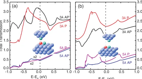
The zero-bias transmission coefficients for the two po-sitions of the tip and at two different tip-dimer distances
HTA are presented in Fig. 2. As expected the transmission
in the tunneling limit (HTA=5 ˚A) is sensitively reduced with
respect to that in the contact limit (HTA=3 ˚A), regardless
of the magnetic arrangement. However, we note that given the different spatial extension of thed andsporbitals, with thed shell being considerably more localized, we expect the tunneling regime to be characterized primarily by tunneling electrons with sp symmetry, while those with d symmetry will contribute the most in the contact limit.
In the tunneling regime, when the Cr tip is above the Co atom of the dimer [see Fig. 2(a)], a peak appears at
−0.3 eV when the spins of the tip and the atom are in the AP configuration, while it is much less pronounced for the P alignment. The transmission coefficient in AP configuration, however, drops near the Fermi level, andT(EF) for the AP
configuration is slightly smaller than that for the P one. In the contact regime, a large transmission peak emerges at −0.15 eV in AP configuration, while it is at −0.4 eV in P one. We then find TP(EF)< TAP(EF), with TP(EF)
[TAP(EF)] being the transmission coefficient atEF for the P
(AP) configuration. Therefore a tip-atom distance-dependent TMR is demonstrated. In order to quantify this effect we define the TMR ratio as
TMR=(IP −IAP)/IAP, (2)
where IP (IAP) is the current in the P (AP) configuration. Note that at zero bias the TMR ratio is obtained in terms of
T(EF) and not of the current, which vanishes. We then obtain
a positive TMR ratio of+14% in the tunneling regime and a negative one of−17% in the contact one. This means that the
-1.0 -0.5 0.0 0.5 1.0
0.0 0.5 1.0 1.5 2.0 2.5 3.0 3.5
-1.0 -0.5 0.0 0.5 1.0
0.0 0.5 1.0 1.5 2.0 2.5 3.0 3.5
E-E F(eV)
3ÅP
3ÅAP
5ÅP
x2
Tota
l
T
ransmission
E-EF(eV)
x2
(a)
5ÅAP
3ÅP
3ÅAP
5ÅP
5ÅAP (b)
FIG. 2. (Color online) Transmission curves for the parallel and antiparallel configurations at zero bias: (a) the Cr tip is positioned above the Co atom; (b) the Cr tip is position above the Cr atom. The numbers in the figure indicate the tip-atom separation. The insets describe the geometry used in the calculation. Note that all energies are measured relatively toEF.
TMR ratio can be tailored by changing tip-atom separations and in particular that a vertical manipulation of the STM tip can change not only the value but also the sign of the TMR.
When the STM tip is positioned above the Cr of the dimer [Fig. 2(b)] the total transmission coefficient in the P configuration is always larger than that of the AP one, in agreement with our previous calculations.30 We thus obtain a positive TMR ratio of about+34% in the tunneling regime and of about+33% in the contact limit. Although the TMR ratio in the tunneling and the contact regime is nearly the same, the transmission coefficient of the former is much less than that of the latter. By comparing Fig.2(a)with Fig.2(b), one finds that, in the contact regime, the transmission coefficient of the tip above Co atom is larger than that calculated when the tip is positioned over Cr, with the TMR ratio changing from−17% to+33%.31In the tunneling regime this change is from+14%
to+34%. This clearly demonstrates that lateral tip movements can produce a change of both the magnitude and the sign of the TMR ratio.
In order to deepen our understanding of the tip-atom distance dependence of the transmission, we concentrate on the configuration where the tip is placed above Co and plot the spin-resolved transmission curves for the P and AP configurations in both the tunneling and the contact regimes (see Figs.3 and 4). For both regimes the majority (↑) AP transmission is larger than that of the P configuration, whereas the minority (↓) AP transmission is smaller than the one of the P. Therefore, the transmission in the AP configuration is mainly determined by majority spins, while the minority spins give the main contribution to the transmission in P configuration. The underlying mechanism for such a transmission features is related to the wave-function overlap between the tip and the atom in two configurations. Such a conclusion can be drawn from the analysis of the orbital projected density of states (PDOS) of the Cr tip and the Co atom in the different regimes. First, we discuss this phenomenon in the tunneling regime. Figures3(c)and3(d)displays the PDOS of thesp orbitals,
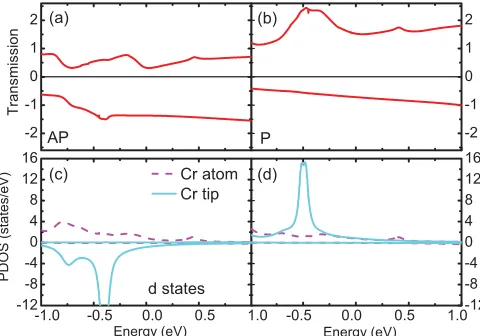
[image:3.608.53.294.539.675.2]FIG. 4. (Color online) Spin-resolved transmission coefficient in the contact regime (HTA=3 ˚A) for the AP (a) and P (b) configurations when the Cr tip is above the Co atom. In the lower panels we show the partial density of states (PDOS) projected over thedorbitals of the Cr tip and the Co atom: (c) AP and (d) P. In all the panels positive values correspond to↑spins and negative values to↓.
which are the ones dominating the tunneling. In the tunneling regime the amplitude of the majority Cosporbitals is nearly the same in the two configurations. In AP configuration the magnitude of the majority Crsp orbitals is larger than that in the P configuration. As a consequence the majority spins contribute the most to the transmission in AP configuration. However, the minority Co and Crspstates in P configuration give a larger contribution to the transmission than the ones in the AP state due to larger contribution of Cr sp states. Furthermore, the total transmission near the Fermi level in AP configuration is slightly smaller than that in the P one [as shown in Fig.2(a)], resulting in a positive TMR ratio.
In the contact regime (Fig.4) thed orbitals of the tip and those of the dimer give a dominant contribution to the electron transport. The d states of the Cr tip and the Co atom are plotted in Figs.4(c)and4(d). In the majority part of the AP configuration there is a pronounced Cr d states located at
−0.5 eV, where a transmission peak is found [see Fig.4(a)]. Therefore, it can be concluded that the transmission peak at
−0.5 eV in Fig.4(a)is mainly caused by Crdstates. It can also be found in Fig.4(c)that in the energy window [−0.3,+0.3] eV there is a strong hybridization betweend states of the tip and those of Co. This is responsible for the robust transmission peaks found around the corresponding energies. Similarly, the transmission peak near+0.5 eV is mainly due to Codstates. In the P configuration, Fig.4(d), although two clear Co majority
dstates appear at−0.25 and+0.3 eV, no significant peak in the transmission is found. In the minority channel, a pronounced minority transmission peak appears at−0.4 eV, which is due to the hybridization between the minoritydstates of the Cr tip and the Codstates. The strong hybridization betweendstates of the Cr tip anddstates of the Co atom is the reason of why at the Fermi level the total transmission coefficient in the AP configuration is larger than that of the P one (see Fig.2), and a negative TMR ratio is obtained.
A similar analysis can also be applied to the case where the Cr tip is above the Cr atom of the dimer, as shown in Fig.5. In
FIG. 5. (Color online) Transmission coefficient in the contact regime for the AP (a) and P (b) configurations when the Cr tip is positioned above the Cr atom of the dimer. In the lower panels we show the partial density of states (PDOS) projected over thedstates of the Cr tip and the Cr atom for both the AP (c) and P (d) configurations. In all panels positive values correspond to↑spins and negative values to↓.
the P configuration in the contact regime, a strong majority transmission peak at −0.5 eV is due to the hybridization between majority Cr tip and Cr atom d states. In contrast, for the AP configuration, the hybridization is weaker in both spin channels, and it results in a reduction of the transmission. Consequently, a positive TMR ratio is observed.
C. Bias-dependent transmission
An inversion of the sign of the TMR ratio has been already demonstrated in magnetic layer structures.32 Furthermore,
recently a spatial modulation of the TMR of a nanostructure has been reported.7However, the same phenomenon has not
been reported for atomic-sized junctions. A closer look at Fig.2(a)reveals that in the tunneling regime forE >−0.05 eV the transmission coefficient in the P configuration is larger
1 1
1
[image:4.608.315.555.70.238.2] [image:4.608.51.293.70.237.2] [image:4.608.313.556.534.700.2]than the one in AP configuration, whereas forE <−0.05 eV it is smaller. Therefore, an inversion of the TMR sign can be expected as the bias increases. Our calculations demonstrate such phenomenon, as shown in Fig.6(a).
The bias dependence of the TMR can be explained by looking at the evolution of the transmission function under bias, which is presented in Figs.6(b)–6(d). Figure6(c)displays the transmission coefficient for the P and AP configurations at zero bias [see also Fig. 2(a)]. At EF the transmission
coefficient in the P configuration is larger than that in the AP one, and a positive TMR is obtained. A strong peak (1) at−0.3 eV appears in AP configuration, and it is due to the interaction betweenspstates of the Cr tip and those of Co [see Fig.3(c)]. Above the Fermi level, the transmission coefficients for both configurations increase linearly. At the positive bias ofV =0.3 V, Fig.6(b), the current is obtained from Eq. (1) by integrating T(E;V) over a bias window. In this energy region the transmission coefficient for the P configuration is always larger than that for the AP one. Therefore,IP > IAP. At that voltage the strong transmission peak (1) in the AP configuration moves down to −0.42 eV, and its shape also changes, as shown in Fig.6(b). However, it does not contribute to the current as it lies outside of the bias window. Thus, at positive biases a positive TMR is found. In contrast, when a negative bias ofV = −0.6 V is applied, as shown in Fig.6(d),
the strong transmission peak (1) in the AP configuration moves to higher energy and enters the bias window, thus contributing significantly to the tunnel current. Therefore, atV = −0.6 V, we haveIAP > IP and the TMR is negative.
IV. CONCLUSIONS
In conclusion, we choose a heteronuclear dimer as a model system to demonstrate that the magnitude and even the sign of the TMR can be tuned by vertical or lateral movements of a spin-polarized STM tip, or even by the external bias. We believe that such a phenomenon is rather general, and it can be found in other transitional metal dimers. Our results are rationalized in terms of the system density of states and the alignment of the various orbital levels under bias. The effect predicted here can probably be proved experimentally by fabricating a magnetic mixed chain on surfaces or producing surfaces with an antiferromagnetic spin structures and by probing it with a spin-polarized STM tip.
ACKNOWLEDGMENTS
SS and IR acknowledge the Science Foundation Ireland (Grant No. 07/IN.1/I945) and the King Abdullah University of Science and Technology (ACRAB project).
1M. Julli´ere,Phys. Lett. A54, 225 (1975).
2J. S. Moodera, Lisa R. Kinder, Terrilyn M. Wong, and R. Meservey,
Phys. Rev. Lett.74, 3273 (1995).
3T. Miyazaki and N. Tezuka, J. Magn. Magn. Mater.139, L231 (1995).
4W. H. Butler, X. G. Zhang, T. C. Schulthess, and J. M. MacLaren,
Phys. Rev. B63, 054416 (2001).
5J. Mathon and A. Umerski, Phys. Rev. B 63, 220403
(2001).
6H. Oka, P. A. Ignatiev, S. Wedekind, G. Rodary, L. Niebergall, V. S. Stepanyuk, D. Sander, and J. Kirschner,Science327, 843 (2010).
7H. Oka, K. Tao, S. Wedekind, G. Rodary, V. S. Stepanyuk, D. Sander, and J. Kirschner, Phys. Rev. Lett. 107, 187201 (2011).
8W. Wulfhekel, M. Klaua, D. Ullmann, F. Zavaliche, J. Kirschner, R. Urban, T. Monchesky, and B. Heinrich,Appl. Phys. Lett.78, 509 (2001).
9S. S. P. Parkin, C. Kaiser, A. Panchula, P. M. Rice, B. Hughes, M. Samant, and S.-H. Yang,Nat. Mater.3, 862 (2004).
10S. Yuasa, T. Nagahama, A. Fukushima, Y. Suzuki, and K. Ando,
Nat. Mater.3, 868 (2004).
11P. Gambardellaet al.,Science300, 1130 (2003).
12Y. Yayon, V. W. Brar, L. Senapati, S. C. Erwin, and M. F. Crommie,
Phys. Rev. Lett.99, 067202 (2007).
13B. W. Heinrich, C. Iacovita, M. V. Rastei, L. Limot, J. P. Bucher, P. A. Ignatiev, V. S. Stepanyuk, and P. Bruno,Phys. Rev. B 79, 113401 (2009).
14F. Meier, L. H. Zhou, J. Wiebe, and R. Wiesendanger,Science320,
82 (2008).
15T. Balashovet al.,Phys. Rev. Lett.102, 257203 (2009).
16J. Brede, N. Atodiresei, S. Kuck, P. Lazi´c, V. Caciuc, Y. Morikawa, G. Hoffmann, S. Bl¨ugel, and R. Wiesendanger, Phys. Rev. Lett.
105, 047204 (2010).
17N. Atodiresei, J. Brede, P. Lazi´c, V. Caciuc, G. Hoffmann, R. Wiesendanger, and S. Bl¨ugel, Phys. Rev. Lett. 105, 066601 (2010).
18A. J. Heinrich, J. A. Gupta, C. P. Lutz, and D. M. Eigler,Science 306, 466 (2004).
19C. F. Hirjibehedin, C.-Y. Lin, A. F. Otte, Markus Ternes, C. P. Lutz, B. A. Jones, and A. J. Heinrich,Science317, 1199 (2007).
20C. F. Hirjibehedin, C. P. Lutz, and A. J. Heinrich,Science312, 1021
(2006).
21T. O. Strandberg, C. M. Canali, and A. H. MacDonald,Nat. Mater. 6, 648 (2007).
22R. Xiao, D. Fritsch, M. D. Kuzmin, K. Koepernik, H. Eschrig, M. Richter, K. Vietze, and G. Seifert,Phys. Rev. Lett.103, 187201 (2009).
23N. N. Negulyaev, V. S. Stepanyuk, W. Hergert, and J. Kirschner,
Phys. Rev. Lett.106, 037202 (2011).
24G. Kresse and J. Hafner, Phys. Rev. B 48, 13115 (1993); 49,
14251 (1994); G. Kresse and J. Furthm¨uller, ibid. 54, 11169 (1996).
25J. P. Perdew and Y. Wang,Phys. Rev. B45, 13244 (1992). 26P. E. Bl¨ochl,Phys. Rev. B50, 17953 (1994).
27A. R. Rocha, V. M. Garc´ıa-Su´arez, S. W. Bailey, C. J. Lambert, J. Ferrer, and S. Sanvito,Phys. Rev. B73, 085414 (2006); Nat. Mater.4, 335 (2004);I. Rungger and S. Sanvito,Phys. Rev. B78, 035407 (2008).
29W. A. Hofer, A. J. Fisher, R. A. Wolkow, and P. Gr¨utter,Phys. Rev.
Lett. 87, 236104 (2001).
30Kun Tao, V. S. Stepanyuk, W. Hergert, I. Rungger, S. Sanvito, and P. Bruno, Phys. Rev. Lett. 103, 057202 (2009).
31We also calculated the transmission coefficient with a pure Cr tip that contains 10 Cr atoms. In the contact regime, when this Cr tip is positioned above the Co atom of the dimer, the TMR ratio is −19.9%, and it is+38.1% when this Cr tip is above the Cr atom of the dimer.
32J. M. De Teresa, A. Barth´el´emy, A. Fert, J. P. Contour, F. Montaigne, and P. Seneor, Science 286, 507 (1999); J. M. De Teresa, A. Barth´el´emy, A. Fert, J. P. Contour, R. Lyonnet, F. Montaigne, P. Seneor, and A. Vaur´es, Phys. Rev. Lett. 82, 4288 (1999);
M. Sharma, S. X. Wang, and J. H. Nickel, ibid.82, 616 (1999);
S. Yuasa, T. Nagahama, and Y. Suzuki,Science297, 234 (2002);