TV
&
CASSETTE INTERFACE
CARD/64 CHARACTER
(llifl@~~
)
"
II
1'\DIGITAL GROUP 1024 CHARACTER TV READOUT/CASSETTE INTERFACE CARD
General Design
This PC Board combines two functions needed by microprocessors, the ability
to output data and messages on a low-cost TV set, and the ability to reliably
store, retrieve, and exchange programs or data at low cost.
The TV Readout
will display 1024 characters, 16 lines of 64 characters per line, with upper
and lower case alpha characters, Greek alphabet, math symbols, and special
characters.
The characters are formed from a 7 x 13 matrix of dots,
pro-ducing easy to read characters with a normal height to width aspect ratio.
The cassette section provided circuits for recording data as well as receiving
data previously recorded.
Frequency Shift Keying is utilized, 2125 Hz being
the Mark of "I" frequency, and 2975 Hz used as the Space or "0" frequency.
The frequency shift keying system gives a better signal/noise ratio and the
wide spacing of the harmonically unrelated frequencies permit the use of low
cost home cassette recorders in spite of their generally poor "wow" and "flutter".
Software parallel to serial conversion systems are used for record, and
software serial to parallel conversion systems for data playback.
These
software conversion systems permit complete flexibility in Data rate (from
near
~
to 1000 bits per second), Codes utilized (ASCII, Baudot, etc.), and
Error checking (parity, CRC, etc.) inclusion.
TV Readout Description
The TV Readout consists of five interacting sections.
They are Memory,
Character Generation, Composite Video Output, Read Clock, and write Clock.
The memory section consists of seven 2102A or faster lK memories, giving
a possible storage of 1024 seven bit ASCII characters.
The microprocessor,
keyboard, or some attached circuit writes the characters one by one into .
the 2102's, and then the TV Readout continuously displays these characters
until either more characters are entered, or the circuit is turned off.
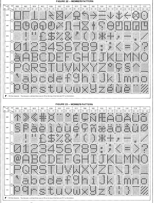
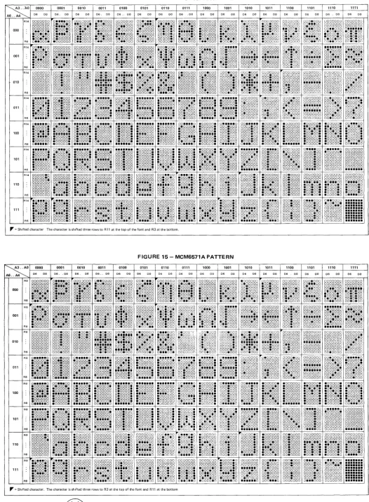
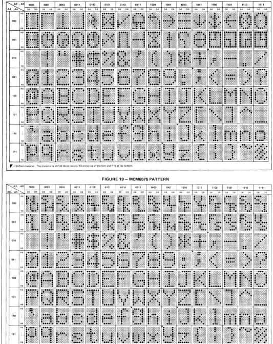
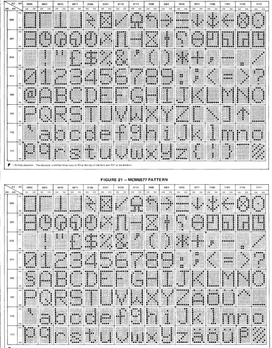
The character generation circuit consists of two IC's, the MCM6571L
char-acter generator, and 74165 parallel to serial converting shift register.
the 6571 takes the seven bit ASCII character coming from the memories and
outputs 7 dots making up a character row for each of 13 potential rows
making up each character.
The 74165 loads these 7 dots coming out at a
time into its internal memory, and then outputs these one at a time for
serial transmission to a TV set.
For more information on TV character
generators, I would suggest reading an excellent article by Don Lancaster'
in June, 1974 Radio-Electronics (p. 48-52).
The video output section uses a 74151 data selector, a 7401 open collector
NAND gate and a driver transistor to produce a low impedence composite
video signal.
The 74151 permits selecting either white characters on a
black background, or black characters on a white background.
In addition
extermal binary level video (such as TV graphics) may be selected/inverted.
The TV output is around 2 volts peak to peak with about a
~volt
horizontal
and vertical sync and blanking pedestal.
~
____________________
C~~_o_@~~_~_@~o~_o~w
____ )
r---~~
The Read Clock is the master control of the various sections.
Starting
from an initial frequency of 11.980 MHz, a countdown chain of three
74193' s (IC's 26, 25, and 37) produce
an~
811s horizontal sync
when gated by 1/6 IC2, 1/2 IC27, 2/3 IC29, and 1/4 IC28.
A 20
l1S
horizontal blanking circuit prevents loss of characters at the edges
of the screen and is produced by the gating action of 3/4 IC17, 1/6 IC2,
and 1/3 IC29.
The resultant horizontal frequency is 15,598 Hz,
some-what lower than the standard 15,750 Hz, but usually only requires trimming
horizontal hold slightly if at all.
The vertical countdown chain uses three more 74193's (IC's 1,15, and 5)
to obtain a final vertical frequency of 60 Hz, syncronous with the AC
line to avoid hum roll and wobble problems on low cost TV's.
3/6 IC7
and IC8 produce an 82011s vertical sync pulse, 2/3 IC6 gives a
~
22 gating
to IC's 15 and 5, and the 1/6 IC7 produces a 3.5ms vertical blanking
pulse.
!"lolII,
:p,:'P'
t~
I"'''''
$y:";:I"f,p..,~ ,~
V-5V+c
flvt
ISf! ,:" ..,-,{,
:';""'1'/
1'J'-re"'A''';,,~
....
I,~.,
H-fy"'1£
p",
IS-f:
"Y(Ju
ItI
",w_~/ty
i-e.
-
II? h-r-/"
-,,,,,-I,:Jf~
/I
J'y~~ d~"""'"
1/
,.~-froc-e.
I,'!'
re'J,-r~~-I"c."
A special feature of this TV Readout board is its ability to be externally
syncronized to an external video timed base.
This permits syncronizing the
microprocessor's video countdown chain to an external video source such as
a TV camera or a commercial TV program for titling, "Frame Grab", etc.
operations.
The horizontal countdown chain is syncronized by a short
negative going pulse appli-ed to connector
pin
U which will reset the
horizontal counters and the horizontal sync pulse.
The Vertical chain
is reset by applying a short negative pulse to connector pin V.
The various Read Clock timings are brought out to the connector so that
external video based systems (such as graphics) may be easily coupled
with this TV system.
As if these operations weren't enough, various timings
from the Read Clock also tell which of the 13 rows, which make up each
character, is being currently accessed, and loads the 74165 when the row
of 7 dots is available from the 6571.
The 11.980 MHz signal then shifts
out 8 dot peroids (the 8th one is a horizontal space between characters)
before the next dot load command
occurs~
All of these timings are very
critical during the design phase, but the builder should have no problems,
since no adjustments are needed.
The Read Clock also controls which of
1024 characters is currently being inputed to the 6571 for dot encoding,
except during Write Clock times.
I thought you'd never ask about the Write Clock.
Well, i t controls the
entry of the characters from whatever external source into the 2102 memory
bank.
Several alternatives in character entry are possible.
However, this
design tries to be as simple as possible, yet give the user a very capable
unit, particularly when using a microprocessor, or even mini, midi, or
ma.xi processors.
A sequential entry system is utilized.
A Home Reset control signal is
developed by IC22 when i t detects the 7 character defining input lines
high ("1").
IC's 23, 13, and 3 are then preset so that the next character
to be entered will result in its being displayed as the top leftmost
character on the screen.
The 2nd character will be viewed to the right
of the first, . . . . until on the 65th character a new line appears, displaying
the 65th character.
Up to 1024 characters are thus
seque~tially
entered
and displayed.
If a 1025th and following characters are entered, an
over-write condition results, with the new page load displayed from the top
. _____________________________
~~
__
o_~~~~~_o~®~~_o~w~~
_____ )
leftmost, the former character overwritten "gone forever".
The display may
be reset at any time.
Screen erase consists of either 1024 or more ASCII
"spaces" (Octal 240) and an ASCII. (all bits on (either a 177 or a 377» ,
or an ASCII. and exactly @.ASCII spaces, the latter being preferable.
r
[U'l-'t
Memory writing occurs when the MSB goes high.
The 74l57's then allow the
74l93's IC23, 13 and 3 in the Write Clock to control the memory address
lines on a priority interrupt basis.
600 ns later, a 600 ns strobe pulse
writes the new character into memory.
WY,d-e.
2dol~55 I~ .j""cvr~""i'~t;(
;1+
,"'1-<..
v"S'I~
-uff,/.""'-;:(l-f~-c.
f<1
01c-tt'(!V1
(/"'5'f3 f'f15f)) (i./!'.
voif1 .... "'Sf
(,,(WC.~'-1
I"w,),
wV',
'!e
p.tA.-.
51
cJd~ c.vt:~-ti-;-1
:;7-
-rc.--,
e
r'l:> I"'j.
~d9,:~
tTl
.L.?l3
r
I
I
r.
rl>
t>
ISIt"'!,
WO,f.;
If /..,
b'~
i>
{,(/(f/th'''jl.,
~{tt"vwr(-r-d':1
;Jrlu::1/,:,a~v
J,-I't~
i, ...
,,-r--c4 ...
VA . .,...'w.·.1f-r: ...
....-dl
",41" , ...
<" ('-
~
i f '1'''>-<~.(Jt:::;rj
_
4-r
-<t..~
,r
v<ff
iJ-r:
I./V, fh'J" ,;v.'ft!'P 0'(:'
-t."'~ '1!~"1Ii1£<)" (~#:>t:t-r:ef,
P,':'/1
hP~
1-tr
W(reft:~
t7J-CV;'c,-<.,,-vv
There is a paraLleL logic path to step the write Clock address forward or
backward without writing a character.
This produces a "Pseudo Cursor"
effect without the usual expense of a number of comparators, etc.
A
software "blink" may be easily implemented with a final result
indistinguish-able from a hardware cursor.
The "Pseudo Cursor" logic consists of 1/4
IC16 and IC38 which detect the presence of an LSB, toggling the Write Clock
,
74193' s up in count without firing the 74L123 (IC20) write Strobe if
:m:R:.-p,~
1"1;'!S
LI
her
simultaneously brought high (indicating character entry then, of course) .
LSB
+
1 high without the MSB toggles the Write Clock 74l93's down in count,
which backs up the cursor.
A 74122 (IC39) produces a short pulse each time the MSB is brought high,
thereby blanking the screen while the memory updating process is taking
place.
This reduces the glitches appearing on the screen when high rate
updating occurs.
The only way to completely eliminate the glitches would
be to only update during the Vertical blanking pulse, but this would
seriously downgrade performance in some critical operations.
Cassette Interface Circuit Description
The previous 512 character Digital Group TVC used a tunable oscillator
which required careful alignment.
This requirement has been eliminated
by using a digital frequency synthesizer countdown chain.
The TV master
oscillator is divided by either 5650 or 4030 to get the 2125 or 2975
cassette frequencies.
The actual frequencies are a few Hertz low, but
well within tolerances.
The main cassette countdown chain consists of
IC's 45, 46, and 43.
IC49 is used to gate an early reset to achieve
the 2125 tone, and IC48 gates an early reset for 2975.
The actual
out-put of this chain is 10 times too high, and the 7490 (IC42) provides a
~
10 smoothing and squaring function.
A logic level input at pin 18 on
the connector controls the resultant audio frequency at output pin 10.
A high input ("1") produces a 2125 Hz output, and a low output
("0")
results in 2975 Hz.
The output wave shape is a symetrical square wave.
The 47K (R13) resistor in series with the output is a typical value to
be used when coupling to the low level, low impedence external microphone
inputs of most cassette recorders.
The cassette receive circuitry detects the prerecorded frequency shift
keying and produces a "1" or a
"0"
output as a result of a detected 2125
Hz or 2975 Hz tone at the input.
IC40 is a clamped limiter which prevents
variations in amplitude from affecting the resultant detection process.
The output of IC40 should be about 1.2 volts p-p, roughly a square wave of
the incoming frequency, constant in amplitude regardless of tape volume
L __
s_e_t_t_i_n_g_o_r_m_i_n_o_r_t_ap_e_'_'
d_r_o_p_ou_t_'_' _p_r_O_b_l_em_s _. _ _ _ (
....
®l®
___
D_@J_O_C®...;;;o;:;...Ut@[]
_ _
o
-..;;®:;..~_o
__
W
_____
)
Two bandpass active filters then amplify a tone 5 times when actually tuned
to their respective frequencies of 2975 Hz for the top filter and 2125 Hz
for the lower filter.
The further
0(;£
the tuned frequency the tone is,
the less amplification the filter will produce.
The actual resonance points
of the filters may be easily adjusted by merely trimming the multiturn
pot-entiometers in each filter.
Full wave active detectors produce rectified full wave pulses at the
sum-ming junction, pin 5 of IC47.
The 2975 Hz tones are rectified
+,
and the 2125
Hz tones are rectified -
As tones depart from either exact frequency,
a value less
+
or - is produced until approximately midway a summed voltage
of
~
results.
A 3-pole lowpass active filter then removes the remaining traces of
pulsating DC from the summed signal with almost no effect on the data
pulses up to a speed of 1000 bits per second.
If lower data rates were
to be utilized, an improved signal to noise ration could be obtained
by multiplying the values of C35, C37, and C38 by the reciprocal of
the data rate difference.
I doubt you would notice any operational difference,
however.
The final section is a slicer connected 741 (IC51).
This op amp detects
whether the voltage at its pin 2 is
+
or - with respect to the constant
voltage at its pin 3.
The output voltage will then swing either to
nearly +5 or to nearly -12.
A forward biased germanium diode prevents
the actual output voltage from going less than
~
-.2 volts, so that valid
TTL levels are not exceeded.
An offset adjusting pot allows the output
to be placed in a "Mark Hold" condition when no tone input is being
detect-ed.
2/4 7400 (IC50) provides output TTL level buffering, and allows
data inversion by tapping the output to the pin 11 section if a customized
circuit required this modification.
Construction
Tools:
Fine tipped, low wattage soldering iron, "wire solder"
(around 20 gauge resin solder), small diagonal cutters.
Test Equipment:
Ohrneter
Audio Generator helpful
10 MHz or better triggered sweep oscilloscope
Frequency Counter
Microprocessor, Mini, etc.
Estimated Construction Time:
3-6 hours
1.
Insert the 24-pin socket, 58-pin sockets, 28 16-pin sockets, and
17 l4-pin sockets into the PC board.
If the sockets have a keyway
indication, orient this away from the connector.
Note:
the top side
of the board is indicated by The Digital Group label.
2.
Invert the board and carefully solder in the sockets.
A special
plating process is used by The Digital Group to minimize solder
joint troubles.
We would suggest a "warmup area" by starting with
the cassette interface sections of the card.
I
~
____________________
(~--Q@-O~-~-O-~~-O-W----)
3.
Insert and solder the 17 resistors in the TV Readout section enclosed
by the +12 bus line.
Insert and solder the 22 resistors in the cassette
section.
4.
Insert and solder the zener diode, the germanium diode, and the 8
silicon diodes.
Note:
all of the diodes are oriented with their
cathode or "bar" end oriented towards the right.
5.
Insert and solder the output transistor in the TV Readout section.
6.
Insert and solder the two 220 pfd and the 330 pfd and the 100 pfd
condensers in the TV Readout section.
7.
Insert and solder the fourteen condensers in the Cassette Interface
section.
8.
Insert and solder the three potentiometers in the Cassette section.
Note that the potentiometer is a 50K, the other two are long
multi-turn 500 ohm units.
9.
Insert and solder the various bypass condensers in the TV Readout
section.
Note:
the positive (+) end of the dipped tantalum
conden-sers is indicated by the vertical marking (paint strip) along one side.
Additional holes have been provided between IC's 9 and 30 for
addition-al input bypassing with 50-200 pfd condensers if your instaddition-allation so
requires.
10.
Trim the crystal socket's pins as shown to fit into the crystal holes.
Pin view:
Result:
Press the rear tab into the board hole provided for it.
Solder the
pins and the rear tab.
The socket provides a space-saving flat mount as well as avoids
sold-ering to the heat-sensitive crystal.
11.
At this point, measure the resistance between ground (pin 20) and the
other voltage supply pins (19, 21,
&
22).
A very low resistance
in-dicates a bad bypass or a solder bridge short somewhere.
12.
Insert the IC's in the TV Readout section except for the memories
(2102's) and the MCM6571L character generator.
The notch or pin 1
end of each IC should be oriented away from the connector end of the
board.
Measure the resistance between pins 19
&
20, noting the value.
Reverse the ohmeter leads and remeasure.
A shorted reading indicates
a bad IC, and near equal readings indicates a reversed IC.
~
____________________
C~@@_o_~~~_~_@~o~_o~w
____
)
13.
Temporarily groung pin 1 of the TV readout and connect a TV set modified
for direct video, or a commercial TV monitor, between pins 16 (video)
and 20 (ground).
14.
Putting a +5 voltage between pins 19 (+) and 20 (Ground) should
result in 64 vertical white columns on the screen.
Refer to "Troubles"
section if this does not happen.
15.
Connect the other ±12 supplies, and turn on power again.
Measure the
voltages on pins 1, 2, and 3 of the MCM6571L socket.
They should
measure -5, +5, and +12 respectively.
16.
Plug in the 2102's and the 6571.
The temporary grounding jumper to
pin 1 should still be connected as well as the
TV
monitor.
Turning on
power this time should result in a random display of 1024 characters on
the screen.
The actual character at each location is determined by the
chance bit structure at the memory locations.
Remove the temporary
grounding jumper from pin 1 when done with this test.
17.
Complete testing of the TV Readout is best performed under microprocessor
control, and sample diagnostic programs are included with The Digital
Group Systems.
"Breadboard diagnostic testing" may be accomplished
temporarily tieing each of pins 2 -
8 to +5 through a lK resistor.
pin 1 to the output of a simple oscillator such as shown below:
.
+5
?
14
,1.
~
1/2
fA
7413
4~
100mfd
+
{f
III
6
>
~220
<;Grounding pins 2 -
8 to ground should produce:
•
pin to ground
Character
8
'\J
7
}
6
{
5
w
4
0
3
2
?
18.
Plug in the twelve IC's in the Cassette section.
19.
Connect a calibrated frequency counter between pin 10 and ground.
by
Tie
20.
Apply +5 and ±12 voltages to the board.
With the Cassette Write input
pin 18 open or tied to +5, the frequency counter should read approximately
2120 Hz.
I
C
~--a
cQJ-o
~-~-o
-®[[@@J-O-W--)
21.
with voltages still applied, ground input pin 18.
The frequency counter
should now read approximately 2970 Hz.
This completes cassette write
turn up.
Easy, isn't it.
22.
Jumper pins 10 and 9 together.
This permits using the write cassette
section as a master oscillator to align the Read Cassette section.
23.
Measure the output at pin 6 of the 741 limiter (IC40) with an oscilloscope.
The waveshape should be an approximate square wave of about .6 volts p-p.
24.
Keeping tpe jumper from ground to connector pin 18, (the frequency
counter should read about 2970 yet) measure the output at pin 7 of
the 5558 active bandpass filter (IC4l).
Turn the 2975 trimmer pot
(R30-the pot in the right corner) until the signal exactly peaks, and
leave at this point.
25.
Move the jumper on connector pin 18 from gorw1d over to +5.
The frequency
counter should now read about 2120.
Measure the output at pin 1 of IC4l.
Turn the 2125 pot (R29-the middle pot) until the signal exactly peaks,
and leave at this point.
26.
Measure the detected voltages at pin 5 of IC47.
When the input
frequency approaches 2125, the output should go -
When approaching 2975,
the output should go +.
Trouble in this area would most likely be caused
by reversed or defective diodes, or adjacent line shorts.
27.
Measure the voltage at the cathode (bar) end of the output clamping
germanium diode (Gl).
If desired, remove the jumpers and attach an
audio oscillator.
Sweeping the frequency between 2125 and 2975 Hz should
result in a clean voltage jump somewhere between 2125 and 2975.
Be sure
that the negativemost voltage at this point is about -.2 volts.
28.
Remove the jumper between pins 9 and 10 and short input pin 9 temporarily
to ground.
Measure the output at pin 6 of IC40 again.
A stable
condition (no oscillation) should be seen.
Connect the oscilloscope
to the cathode of Gl again.
Adjust the balance potentiometer (R18
-the small leftmost pot) clockwise so that -the voltage is at a -
level.
Slowly turn the potentiometer counterclockwise until the voltage jumps
+ and leave setting at this point.
29.
Disconnect the temporary jumper from conncector pin 9 and reconnect
the audio oscillator.
Perform step 24 again.
If all proceeds well
at this point, the cassette interface is ready to receive data.
Troubles - General
1.
One of the more difficult troubles to find is an IC pin which was bent
under the IC when i t was inserted.
Any unusual pressure when inserting
an IC should be investigated.
2.
Every pin should be soldered.
The most frequent cause of trouble is
an unsoldered pin, generally an end IC pin.
Carefully sighting down
parallel rows of pins usually finds any that are not soldered.
3.
When troubleshooting with a 'scope probe, measure from the top side of
the IC, not the bottom, to eliminate a bent under pin problem or defective
socket from misleading.
r;
)
---'---~
4.
Before ever plugging in any IC's, always measure the voltages at the PC
board and at the pins of the more expensive IC's, like the 6571.
5.
When handling IC's, avoid static charges.
Run your house humidity high,
and ground yourself ty touching a grounded chassis before touching Ie's.
6.
Beware of solder splashes and drilling errors. Please inform The Digital
Group of board manufacturing errors that you detect.
A flashover or splash
on the topside would be very difficult to find after soldering the sockets.
The black socket body of the sockets used in The Digital Group kits may
be pried off after removing the IC should a hidden splash be suspected.
7.
Beware of shorts in the cassette area between component leads and
under-lying circuitry.
Specific Troubles
No white colums on the screen at step 14.
1.
Bad connection between connector pin 16 and TV.
2.
Temporary jumper from connector pin 1 to ground not connected.
3.
Crystal not oscillating.
Check for pulses at pin 1 of ICl6.
4.
Horizontal Countdown chain defective.
Successively measure output
at pin 3 of IC's 26, 25, and 37.
Each should be progressively lower
in frequency.
5.
Vertical Countdown chain defective.
As above #4, but measure IC's
1, 15, and 5.
6.
Defective video mixer.
Look for pulses at pins 1 and 13 of IC19.
Poor or lacking syncronization at step 14.
1.
TV is overloaded by the
~
3 volts of video.
Swamp the video with
a 10 ohm resistor to see of sync
& video stabilizes.
2.
Check for Horizontal and vertical sync and blanking pulses at
connector pin 16.
A 75 ohm load should be attached.
The pattern
should look like:
sync
a.
If Horizontal Sync is defective, check IC's 2, 27, 2S, and 29.
b.
If vertical Sync is defective, check IC's 7 and S.
c.
If Horizontal Blank, check IC's 2, 17, and 29.
d.
If vertical Blank, IC7.
No characters at Step 16.
1.
Missing voltages at the MCM6571 (ICll).
2.
Defective Character generator.
3.
Defective 74165 (ICIO) or 74157 (IClS).
4.
Defective logic signals to and from ICll and ICIO.
All inputs and
outputs should be pulsing at valid TTL levels
(~
to .S volts
=
low/ 2 to 5 volts
=
high).
5.
Pins 11 and 10 of 74151 (IClS) not at +5.
~
____________________
~~~_=_~~~o~_o~~_~~w~
__ )
Wrong character(s) in display
1.
Miswired or misjurnpered input.
2.
Defective Memory IC.
Note:
the bit difference between the intended
character.
IC30 is the memory for the Least Significant Bit (LSB)
of the character ... and IC36 is the Most Significant Bit's (MSB)
memory.
3.
Defective 74l57(s) -
IC's 24, 14, and 4.
4.
Shorted lines in the memory and write clock area.
"Twinkling" character on TV
1.
Slow memories.
500 nanoseconds or faster 2102's must be used.
2.
Overheated memories.
Access times increase with heat.
3.
Slow 657lL - none seen so far, but possible.
Uneven lighting of leading and trailing edges of characters, esp. "H".
1.
Monitor bandwidth too low produces a dim left side of H, bright on
the horizontal bar part.
2.
Incorrectly high peaked monitors give an excessively bright left edge
to characters such as "H".
3.
Dim right side of "H" and other characters may be monitor or may
re-quire increasing the clock lag condenser (IC43) in value.
Too
high of a value will reduce the left side of characters such as "H".
Won't write characters
1.
Missing Storbe pulse, or continuous level on MSB input
(~onnector
pin 1).
2.
No write pulse from 74L123 (IC20).
Measure at pin 12 of IC20,
looking for an
~
600 ns negative going pulse.
Connecting the MSB
(connector pin 1) to a
~50KHz
TTL clock will permit viewing on
lower cost oscilloscopes.
3.
write Clock not toggling.
With above temporary oscillator inputting
to MSB, look for pulses at pin 3 of IC's 23, 13, and 3.
4.
Defective Read/Write Multiplexers (IC's 24, 14, and 4.
Extraneous Characters
1.
Noise on the input lines to the memory, particularly on the MSB
(connector pin 1).
Pads for Cl, C2, and C3 -
small pfd condensers
used on the input line to suppress most noise sources.
This trouble
generally shows up as an a appearing on the screen when another port
is addressed.
2.
Data sent to the TV character generator faster than i t can handle.
Data must be valid for 1.S microseconds following the rise of MSB
strobe.
Faster data rates can be handled by reducing the value of the
condensers in the 74L123 (IC20) write strobe singleshot.
Alter-natively, a data hold loop consisting of Nap's can slow the data
out-put to the readout.
3.
Defective or slow memories.
Look at the bit pattern of the extraneous
character to determine if a single memory is bad.
4.
More bypassing required.
A number of unused voltage bypassing pads
at the top of the TV Readout section have been included should
your particular system require them.
Defective level output from Cassette Input Limiter
1.
None at all:
Check for ±12 to IC40.
2.
Too high output level.
Diodes (S3 and S4) open or one is reversed.
Bandpass Active Filter Problems
1.
Check by sweeping with audio oscillator for proper range.
2.
Swap 5558 (IC4l) with IC's 44 and 47.
3.
Check for shorts or out of tolerance (5%) condensers C30, C31, C32,
or C33.
Disc ceramics are a no-no in tuned circuits!
Full Wave Detector
1.
Diodes open, reversed or shorted.
2.
Defective 5558 (IC44).
Low Pass Active Filter
1.
Shorted or out of tolerance condensers.
2.
Defective IC47.
output Slicer (IC38)
1.
Reversed, open, or not Germanium diode at Gl.
2.
Defective or missoldered resistors in pin 3 circuitry of 741 (IC5l).
3.
Defective 741 (IC5l).
' - - - -_ _ _ _ _ _ _ _ _ _
\.--C
iliJL@_o
_cQJ~-=-o
[K@]_o
---=-®_[f@}D~W_'_____)
1024 CHARACTER READOUT
& CASSETTE INTERFACE - PARTS LIST
rc's
rC30,36
rCll
rC9, 17, 28, 50
rC19
IC16
IC2, 7
rC6, 29
IC27
rC8, 22, 48, 49
IC42
Capacitors
C2
C4, 5
C43
C24
C35
C30 - C33
C37
C38
Bypass Capacitors
24
.01 mfd disc
4 -
1 mfd tanta1ums
Crystal
1 -
11.980 MHz
Resistors
-
all
~
watt 5%
Rll
R12
R31
Rl, 2, 10
R28
R32
R5, 42
R6, 7, 8, 9, 14
R22
R3, 4
7 -
2102-1 or better
1 - MCM6571L
4 -
7400
1 -
7401
1 -
7402
2 -
7404
2 -
7410
I -
7420
4 -
7430
1 -
7490
1 -
100 pfd mica
2 -
100 pfd mica
1 -
330 pfd mica
1 -
1000 pfd mica
I -
.0047 mylar
4 -
.01 polystyrene
(may be marked 10000)
1 -
.01 mylar
I -
.015 mylar
Misc
5 -
8 pin sockets
17 -
14 pin sockets
28 -
16 pin sockets
1 -
24 pin sockets
I -
crystal holder
1 - documentation
unless noted
1 -
22 ohm
1 -
220 ohm
1 -
390 ohm
3 -
470 ohm
1 -
470 ohm
~
watt
1 -
620 ohm
2
-
lK
5 -
2.2K
1 -
4.7K
2
-
15k
IC's
IC39
1 - 74122
IC20, 38
2
-
74L123
IC18
1 -
74151
IC4, 14, 24
3 -
74157
ICIO
1 -
74165
rCl, 3, 5, 12, 13,
14 -
74193
15, 21, 23, 25,
26, 37, 43, 45
46
IC40, 51
2 -
741
rC41, 44, 47
3 - 5558 or LM1458
Diodes
Sl - S8
8 -
IN914 or IN4148
Gl
1 -
IN48 or eq.
Germanium
ZI
1 -
5V 1 watt zener
(lN4733 or eq.)
Tl
1 -
2N5129/2N2369
Resistors
R16, 17, 19, 20, 21, 26,
11 -
10K
27, 35, 36, 37, 38
R15
1 -
33K
R13, 24, 25, 33
4 -
47K
R34
1 -
68K
R39, 40, 41
3 -
lOOK
R29, 30
2 -
500rt trimpot
R18
1 -
50K pot
1024 Character TVC
Front of Board
Pin Side of Board
Pin
Function
Pin
Function
1
MSB
Strobe
A
P
2
MSB
B
A
3
MSB
C
B
4
MSB
Data to TV
D
C
Harz
5
MSB
E
D
6
MSB
F
E
7
MSB
H
N
8
LSB
J
F
9
Data from Cassette
K
G
10
Data to Cassette
L
H
11
Clock
M
I
Vert
12
H sync
N
J
13
V sync
P
K
14
H Blank
R
L
15
V Blank
S
M
16
Video
T
Data Inv
17
Data to CPU
U
H Preset
18
Data from CPU
V
V Preset
19
+5
W
Graphic Input
20
Ground
X
Graphic Select
21
+12
Y
not used
22
-12
Z
1
~
___________________________
C~--o-@-~-~-o-®-o~-o--w---)
512 TO 1024 UPGRADE SPECIAL DIRECTIONS
This 512 to 1024 character upgrade kit permits using most of the 512
character IC's in addition to a new board, sockets, resistors, condensers
and miscellaneous parts to achieve a 1024 character TV readout.
Steps:
1.
Remove all IC's from your 512 board except IC27 (74LOO), IC23 (74123),
and IC33 (566).
2,.
Add the 34 IC's just removed to the IC' s supplied with the 1024
character upgrade kit.
3.
Continue with regular 1024 character readout directions.
l . . - - -_ _ _ _ _ _ _ _ _ _ _
c
L-@l@_-
o_cQ]~l®_~___.:~~o
_0
-::::;:;.0 _ _ _
)
1024 CHARACTER READOUT
& CASSETTE INTERFACE UPGRADE - PARTS LIST
IC's
(IC30, 36)
7 -
2102-1 or better
(Iel1)
1 - MCM6571L
IC9, 17 (28, 50)
4 -
7400
( IC19)
1 -
7401
IC16
1 -
7402
(IC2, 7)
2 -
7404
IC6, (29)
2 -
7410
(IC27)
1 -
7420
IC8, 22, (48, 49) 4 - 7430
IC42
1 -
7490
Capacitors
C2
1 - 100 pfd mica
C4, 5
2 -
220 pfd mica
C43
1 - 330 pfd mica
C24
1 -
1000 pfd mica
C35
1 -
.0047 mylar
C30 - C33
4 -
.01 polystyrene
(may be marked 10000)
C37
1 -
.01 mylar
C38
1 -
.015 mylar
Bypass Capacitors
Misc
24 -
.01 mfd disc
5 -
8 pin sockets
4
-
1 mfd tantalwns 17 -
14 pin sockets
Crystal
1 - 11.980 MHz
28 -
16 pin sockets
1 -
24 pin sockets
1 -
crystal holder
1 - documentation
Resistors - all \ watt 5% unless noted
Rl1
1 -
22 ohm
R12
1 -
220 ohm
R31
1 -
390 ohm
Rl, 2, 10
R28
R32
R5, 42
R6 , 7, 8 , 9 , 14
R22
R3, 4, 22
3
1
1
2
470 ohm
470 ohm
~
watt
620 ohm
lK
5
2.2K
1 -
4.7K
3 -
6.8K
IC's
IC39
1 -
74122
IC20, 38
2 -
74L123
IC18
1 - 74151
(IC4, 14, 24)
3 - 74157
(IC10)
1 - 74165
IC1, 3, 5, 12, 13,
14 - 74193
15, 21, 23, 25
(26, 37, 43, 45,
46)
(IC40, 51)
2 - 741
(IC41, 44, 47)
3 - 5558 or LM1458
Diodes
Sl - S8
8 - IN914 or IN4148
Gl
1 - IN48 or eq.
Germanium
Zl
1 -
5V 1 watt zener
(lN4733 or eq.)
T1
1 -
2N5129/2N2369
Resistors
R16, 17, 19, 20, 21, 26, 11 - 10K
27, 35, 36, 37, 38
Rl5
1 -
33K
R13, 24, 25, 33
4 - 47K
R34
1 - 68K
R39, 40, 41
3 - lOOK
R29, 30
2
-
500Q
trimpot
R18
1 - 50K pot
( ) indicates IC's removed from 512 Character Readout and Cassette Interface
'----_ _ _ _ _ _ _ _ _ _
~(m_o_cQ]~_=__o~_o__=_®_~__._;;;;..W~_)
, I
NOTE TO OWNERS OF THE PREVIOUS 512 CHARACTER TVC-F.
The 1024 character TV readout board produces 64 characters on each horizontal line
now, instead of the previous 32 per line.
This will generally result in a need for
reprogramming the screen formatting somewhat.
Most D.G.S.S. Z-80
tapes
using 512
character TV output have been modified to reflect this additional character count
requirement.
However, user designed programs may have to be modified to support
the additional characters.
A "quick and dirty" implementation can be performed
by outputting an additional space lIafter each character or space."
The screen erase subroutine must output 1024 spaces.
This subroutine is part of
the EROM op system of the various Digital Group CPU boards.
The Z-80 has had
several versions of EROM supplied, marked ZA, ZB, ZC, ZD, and ZE.
ZE is the latest
and most cornmon.
All but the ZA version already perform a correct "Erase" for both
the 1024 and the 512 character TVC's.
The 8080, 68000r 6502, (or 6501) must have 80B, 68B or 6502, respectively, EROM's
to satisfactorily perform a 1024 character Erase.
Should you have an older 512 character erasing EROM (a very small number of
customers are in this category) please return your EROM and the Digital Group will
reprogram/exchange i t with the latest version for $5.00 postpaid .
. ; I ,
~
_____________________
(~@@_a_~~~_~_@~o~_o~w
____ )
L - _ - ;
____
~___
r__----.L
---,-: