BM792
read-only-memory
and MR11-DB
bootstrap loade"r
1st Edition, July 1971 2nd Printing, December 1971 3rd Printing (Rev), October 1972 4th Printing, December 1972 5th Printing, May 1973
6th Printing (Rev), January 1l)74 7th Printing, August 1974 8th Printing, January 1975
Copyright © 1971, 1972, 1973. 1974. and 1975 by Digital Equipment Corporation
TIll' matl'rial in this manual is for informational purposes and is subject to change without notice.
Printed in U.S.A.
Th~ following are trademarks of Digital Equipment
Corporation. Maynard, Massachusetts:
DEC
FLIP CHIP
DIGITAL
PDP
FOCAL
CONTENTS
CHAPTER 1 INTRODUCTION
1.1 1.2
SCOPE
GENERAL DESCRIPTION
CHAPTER 2 DETAILED DESCRIPTION
,~. 1
"
.,
.~ . .32.4
~.5
BASIC OPERATION ADDRESS SELECTION
, WORD SELECTION
DIonE MATRIX AND OUTPUT BUFFER
ANODE RECOVERY CIRCUIT
CHAPTER 3 PROGRAMMING AND OPERATION
3.1 .L2
GENERAL
PROGRAMMING THE ROM
CHAPTER 4 ROM ENGINEERING DRAWINGS
APPENDIX A BM792-YA PAPER-TAPE BOOTSTRAP LOADER
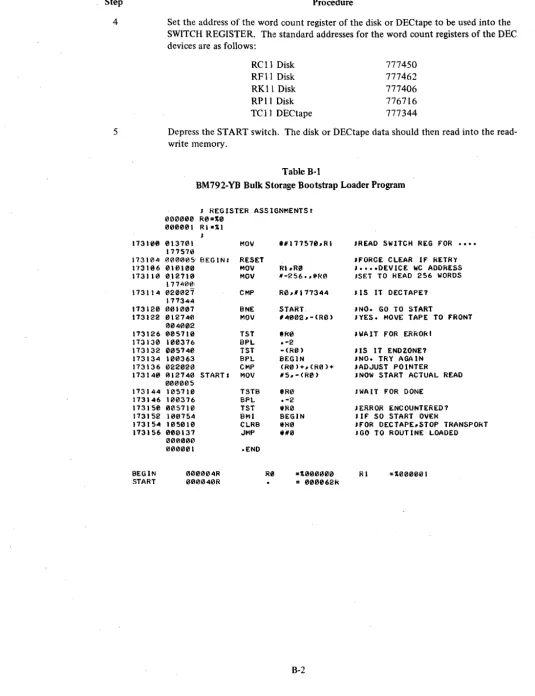
APPENDIX D BM792-YB BULK STORAGE BOOTSTRAP LOADER
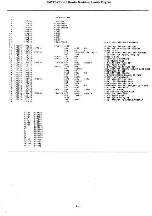
APPENDIX C BM792-YC CARD READER BOOTSTRAP LOADER
APPENDIX D MRII-DB BULK STORAGE BOOTSTRAP LOADER
APPENDIX E BM792-YF BULK STORAGE BOOTSTRAP LOADER
,\PPENDIX F BM792-YH CASSETTE BOOTSTRAP LOADER
Figure No.
2-1 2-2 2-3
2-4 2-5
2-6
3-1
ILLUSTRATIONS
Title
ROM Block Diagram ROM Address Word Format
Simplified Logic Diagram of ROM Address Selection Circuits for Addresses 773400 - 773476
Word Selection Circuit for 773X04 Address
Diode Matrix and Output Buffer, Simplified Logic Diagram Anode Recovery Circuit
Physical Locations of Addresses and Bits in the ROM Diode Matrix
1-1 1--\
::1 2-\
.,
,.. -~"
3-1
3-1
2-t 2-2
2-3
2-4
2-5
2-6
Table No.
\- t ~-I
'-
.,
A-I
B-1
C-I \)-\D-~ 0-3
E-I
F-I
Pn .. ·programmed ROMs ROM Addn~ssl's
B('I) Ikcolkr Truth Tahk
TABLES
Title
BM 7l) ~-VA Pap~r-Tap~ Bootst rap Loader l')rogram
BM79::!-YB Bulk Storage Bootstrap Loader Program BM792-YC Card R~ad~1' Bootstrap Loader Program M R II-DB Bulk Storage Program Loader Listing Starting Address
Power Up Start Vector Jumper Connections BM792-YF Bulk Storag'~.Bootstrap Loader Program BM792-YH Cassette Bootstrap Loader Program
Page
1-2
A-3 B-~ ('-3
\)-3
0-4
CHAPTER 1
INTRODUCTION
1.1 SCOPE
This manual provides the lIscr with theory of operation, programming information, and schematics necessary to understand and program the BM792 Read-Only-Memory (ROM). The level of discussion assumes that the reader
is familiar with basic digital computer theory.
Although the input and output signals of the ROM are carried by the Unibus
@ ,
it is beyond the scope of this manual to describe the Unibus itself. A detailed description of the Unibus is presented in the PDP-Ii PeripheralsHandbook.
1.2 GENERAL DESCRIPTION
The BM792 is a 32-word read-only-memory (ROM). The diode matrix and address selection circuits that consti-tute the ROM are mounted on an extra-width quad-board module. This module is inserted in either one of the two small peripheral controller slots in the PDP-II processor or in one of the four slots in the DD-II peripheral mounting panel.
The ROM is available either unprogrammed (designated BM792) or preprogrammed (designated BM792-Y X. where the letter in the X position identifies the program). The unprogrammed module can be programmed to form code conversion tables or contain frequently-used mathematical values and subroutines. These applications of the ROM provide an access time of 100 ns, which can increase the program speed.
Preprogrammed ROMs are used for implementing small standard programs required in PDP-II System opl'ration. such as bootstrap loaders for paper tape or DECtape. The preprogrammed ROMs that are available at
puhlica-tion of this manual are described in the Appendices and listed in Table 1-1. As addipuhlica-tional preprogrammed ROMs become available, additional appendices will be published to describe them.
Module
I
Option No. of Words.M792-YA BM792-YA ~,
M792-YB BM792-YB 32
M792-YC BM792-YC 32
M792-YD MRII-DB 64
M792-YE
M792-YF BM792-YF 32
M792-YH BM792-YH 32
...
N
I
I
Table I-I Preprogrammed ROMs
Power-Up
Address Range Vector
-.
773000-773077
I
No773 I 00-773 I 77
No
773200-773277 No
773 1 00-773277 Yes
(Ex-cept TM)
773200-773277
No
773300-773377 Yes
I
!
No. 01 Worth I II
Devices I{cad-In Loading AreaI i
KL nL-A, I ()2 max. Highest Memory
I
DL-B, PC, PRTC, RC, RF, 256
o
and upRK, RP
CR, CM Variahle Variable
TC, TM, RC', TM:256
o
and upRF, RK, RP Othcrs:512
TC,RK,RF 25()
o
and upTA 64 (\ ~-..I , ,
CHAPTER 2
DETAILED DESCRIPTION
2.1 BASIC OPERATION.
Th~ ROM diode matrix contains 32 16-bit words, ~ach of which can be applied to the bus under program control.
The ROM responds only to a DATI from the Unibus, DATO, DATOB, and DATIP are ignored. A block diagram
of the ROM is shown in Figure 2-1.
When both a DATI and a ROM address '}fl' sent to the ROM, the word in the addressed location of the diod~
matrix is applied to the Unibus. When th~ ROM address is received. the 5-bit,code on address linl's AO I through
A05 is decoded to apply a signal to the cathodes of the diodes in the addressed word location. The word in the
addressed location is transferred through the output buffer to data lines DOO through 015 of thl' Unibus.
UNIBUS
2.1 ADDRESS SELECTION
~---~.---~ ______ ~ADDRESS~ ______ ~ A <06: 17> SELECTOR ANODE
RECOVERY DAT I
MSYN SSYN
~-..----' SIGNAL
WORD
A <01:05> SELECTOR CATHODE
D<OO: 15>
DRIVER SIGNAL
32 x 16 DIODE MATRIX
Figure 2-1 ROM Block Diagram
---+ OUTPUT BUFFER
1\ -02 99
TIll' addr~'ss \\onl formal for the ROM is shown in Figure 2-2. Octal addresses for the ROM must he or the
--:-JXXX j'orm:lt. Thc ROM reads-out only full 16-bit words and docs not issue byte data; thus, address hit AOO
j.., Il () t lI,>~.'d,
(he addr\.'..,\c:-. arc i'urtiler divided into eight groups, which are determined by address bits A08, A07, alld AO() ;lI1d
[image:7.612.76.503.334.613.2]WORD SELECTION ADDRESS 8x4 =
32
OCTAL GROUP r ---~
ADORES S
7
7
3
0-7
0-7
0-7
r-~r--~~"---'---"'~~
ADOREB~~
\17 \16\15\14\13\12111
\10\09\08\07106\05\04\03102\ 01\
Figure 2-2 ROM Address Word Format
Address Word Bit
A08 A07
0 0
0 0
0 1
0 1
1 0
1 0
1 1
1 1
A06
0
1
0
1
0
1
0
1
Table 2-1
ROM Addresses
Address Ranges
773000 - 773076
773 1 00 - 773 I 76
773200 - 773276
773300 - 773376
773400 - 773476
773500 - 773576
773600 - 773676
773700 - 773776
Preprogram med
ROMs
BM792-YA
BM792-YB, YD
BM792-YC, YE, YF
BM792-YH
11-0298
In a PDP-l 1 Syst~m. only ant? ROM module can be used for each of the eight address groups. Jumpers on the
module art? connected in a configuration that causes the module to respond to its designated address group.
For exampk. when a ROM modull' is to be addressed in the group 773400 - 773476, bits A08, A07. and AO() of
the address word contain binary 100 as shown inTable 2-1. The bus lint's for these bits an: shown COt1Ill'dl'd to the circuits of the ROM in Figure 2-3, a simplified logic diagram of the address selection circuits. Figure 2-3 abo shows the address selection circuit jumpers connected to respond to address group 773400 - 773476. Asserted
bus lilll'S arc low and ullasserted bus lines arc high, so that the output of gate F 12 at pin 14 is high and the outputs of pins .2 and 3 arc low when a valid address is received. Each of the three outputs from the E 12 gates is exclusive
NORed with a low or a high level, depending 011 the jumper configuration. The outputs of the three E 13 gates
must ill' high to accomplish address selection; therefore, the jumper configuration shown responds to addresses in
the 773400 - 773476 group.
The signal, which results from the decoding of bits A08, A07, and A06, is gated with a signal generated by the
decoding of an address in the format 773XXX and receiving MSYN (Drawing D-CS-M792-0-1). The resulting
signal (pin 10 of gate E 17) is gated with a signal generated by the decoding of a DATIon the control lines.
Therefore, pin 8 of gate El7 provides a low output signal when the ROM address, MSYN, and DATI are asserted
on the bus. This signal at pin 8 is uscd to accomplish thc following in thc ROM circuits (sec Drawing
D-CS-M792-0-1 ):
I. Assert SSYN on the bus.
} Activate the word selection circuits.
[image:8.612.42.531.58.397.2] [image:8.612.35.537.60.729.2]+ 5V NO __ ~
PIN L ; 9
8
~~~.
- - W3
eN 2 BUS AO 8 L 10 E 1 ;> ~~._~_-=-~~
______
~__
9+5V
JUMPER
o CP2
PIN'~7_
2~
- W2- BUS A07L 6 E12 - - - 1
+5V
PIN H
~
~
o C U 1B -U-S-A-O-6-~f--3 _ _ _ -_-___ W_' _ _ 2-/)
H
E13 TRUTH TABLE EXCLUSIVE NOR
A B C
L L H
L H L
H L L
H H H
11-0297
Figure 2-3 Simplified Logic Diagram of ROM Address Selection Circuits for Addresses 773400 - 773476
2.3 WORD SELECTION
Bits AOS - AO I of the address word are decoded by the word selection circuits to select Olle of the 32 word lo-cations in the diode matrix. A low-level signal is then applied to the diodes in the addressed word location,
re-sulting in 16 bits of data being read out on the data bus lines.
Because address bit AOO is not connected to the ROM, byte addressing is ignored and a 16-bit word is read onto the bus regardless of the state of AOO. In the octal coding of the address, AOO is considered in designating the last octal digit. Therefore, the addresses of the words in the ROM use the following sequence:
773XOO 773X02 773X04 773X06 773XIO 773X12 etc.
An address of 773XO 1 would address the same location as 773XOO, and 773X03 would be the same as location 733X02.
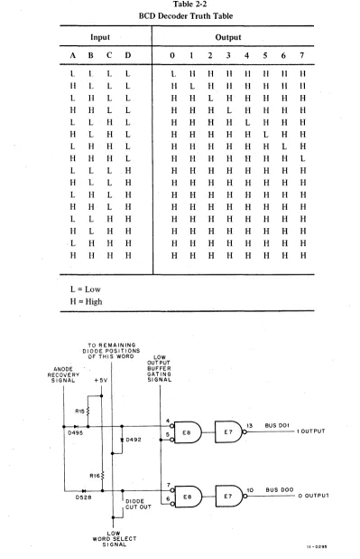
A simplified logic diagram for the word selection circuits is shown in Figure 2-4. This diagram illustrates how the circuits operate for a 773X04 address. Table 2-2 is a truth table for the Binary-Coded Decimal (BCD) de-coders that are shown in the diagram and on Drawing O-CS-M792-0-1.
[image:9.612.76.494.49.258.2]the ROM. The signal levels on the cathodes of the other 31 word locations are high. Thus, only the diodes in location 04 arc forward-biased, allowing the word in this location to be read by the output buffers and applied to
the Unibus.
TO CATHODES OF DIODES IN LOCATION 04
773X04
°
IH'~us
'0'
L~
EIGY---.--..
---.---BUS A02 L
-~1:3---_---~
, (Llo (HI BUS AOI L _~~ _ _ _ _ _ _
~---.
O(H) J!~A04L;al1
E 14 .f-C-13=--_ _ _ _ _ _=_; 12
L
o (H) B U S A O S L ; G S
E 14 .f-"':3 _ _ _ . - - J
4
I
FROM s~~~~ig~ - - - - , - L7
0Wc:-:-:W7:CH:":"":E::-:"N:-7==7=-=3::-:"X7:CX X:-:-:"A"::"O=-=DR=-=E::::S"::"S,---' MSYN. 8 DATI ARE RECEIVED
L
L
L A
B EI8 BCOI C
D o L
1
2
:3
Figure 2-4 Word Selection Circuit for 773X04 Address
2.4 DIODE MATRIX AND OUTPUT BUFFER
A B C D L H L L
"-0296
The BM792 ROM is supplied with a complete diode matrix. A diode is wired into each of the 16-bit locations of all 32 words. The binary content of each word is determined by the presence or absence of the diodes: thus..
the lIser can program the module by cutting Ollt selected diodes. Presence of a diode in a bit location produces
a binary 1 and absence produces a binary O. The pre programmed ROMs are manufactured with the diode con-figuration required for their programs.
A simplified logic diagram of the diode matrix and the output buffer is illustrated in Figure 2-S. The low output buffer gating signal is present when the ROM address, MSYN, and DATI are asserted on the bus (refer to
Para-graph 2.2). Th.e word select signal is low when the particular word location is selected by the decoding of bits AOS - AOI (refer to Paragraph 2.3).
Diode D492 for the DO I bit is in the circuit and is forward-biased. Therefore, a low level is gated with the out-put buffer gating signal,which results in the assertion of a low level on bus line DOl to signify a binary 1. The diode for the DOO bit is cut out of the circuit. Therefore,
a
high-level signal is gated with the output buffer gat-ing signal, which results in the assertion of a high level on bus line DOO to signify a binary O. The remaingat-ing bit [image:10.611.75.518.90.355.2]Table 2-2 BCD Decoder Truth Table
Input
A B
L L
II L
L H
H H
L L
H L
L H
H H
L L
H L
L H
H H
L L
H L ·L H
H H
L= Low H = High
C L L L L H
H
H H L L L L H H H H D L L L L L L L L .H H H H H H H HTO REMAINING DIODE POSITIONS
OF THIS WORD ANODE
RECOVERY
SIGNAL +5V
I R15 0 L H H H H H H H LOW OUTPUT BUFFER
GAT I N G
51 GNAL H H H H H H H H 1 H L H H H H H H H H H H H H H H Output
2 3
H 11
H II
L H
H L
H H
H H
H H
H H
H H
H H
H H
H H
H H
H H
H H
H H
4 5 6 7
II II II II
H
H II IIH H H H
H
H
HH
L H H H
H L H H
H H L
if
H H H L
H H H H
H H H H
H
H H HH H H H
H H H H
H H H H
H H H H
H H H H
13 BUS DOl
0495 1 OUTPUT
0492
RIG
0528
DIODE CUT OUT
LOW WORD SELECT
SIGNAL
10 BUS 000
0 - - - 0 OUTPUl
II - 0295
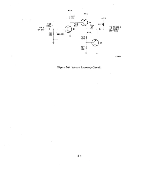
[image:11.612.98.498.53.672.2]2.5 ANODE RECOVERY CIRCUIT
The anode recovery circuit (see Figure 2-6) provides a voltage surge to the anodes of the diodes in the matrix immediately after a word is read out. This voltage surge charges the capacitance of the diode in the matrix and
ensures that the anode lines in the matrix are at a high level for the next read out.
Transistors Q I. Q~. and QJ (St'e Figure ~-6) art' tUflll'd 01'1' when thl' ROM is IIl)1 being addn.'ssl'd. Pin ~ llf F I 7
gOt'S fWIll low tn high wlll'1l the bus addressing signals arc conduded. The high signal turns on Q 1 and subsequently Q2, which provides the positivr voltage surge to the anodes of the diodes in the matrix.
Transistor Q3 of the anode recovery circuit is used as a clamp. When the voltage surge from the collector of Q2
reaches a high enough value, Q3 turns on and grounds out the surge.
+5V
+5V R25
2K
R24 1.5K ) 01
R28 100
R27 100
+5V
8.2K 02
R26
47 TO ANODES
~-""""r-_ _ " " " _ -OF DIODE MATRIX +5V
03
[image:12.611.39.509.193.764.2]11-0367
CHAPTER 3
PROGRAMMING AND OPERATION
3.1 GENERAL
The ROM operates in a manner similar to other memory devices that can be included in a PDP-II system. When the ROM is used for storage of constants, the processor may be programmed to address the appropriate ROM location for the required constant. When the ROM is used for storage of a subroutine, a jump instruction is used to get into the subroutine and place the first address in the program counter. Then the program counter is changed to address the other sequential steps in the subroutine. The last step of a subroutine stored on the ROM should be either a jump instruction to a location out of the ROM or a return from subroutine instruction.
3.2 PROGRAMMING THE ROM
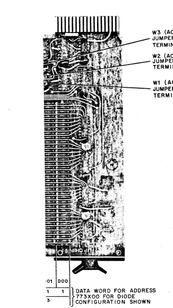
Programming the ROM is accomplished by cutting diodes out of the diode matrix in the configuration required
for the binary data words to be used. The diode must be removed for each bit position that is to read out as a binary O.
The physical orientation of the diode matrix with respect to the addresses and the bit positions is shown in Figure 3-1. Address 773XOO is shown with diodes removed in a configuration that reads out the binary word 1 010010
011 101 011. With Figure 3-1 and a binary listing of up to 32 16-bit words, the user can program his ROM mod-ule.
The ROM module must also be programmed to respond to one of the address groups determined by address bits A08, A07, and A06 (refer to Table 2-1). Figure 3-1 shows the locations of the three sets of address-bit jumper terminals which are labeled WI, W2, and W3 on the ROM printed circuit board. The relationship between the jumper tenninals and the address bit is as follows:
WI A06
W2 A07
W3 A08
101 000
W3
(A08)
JUMPER TERMINALS
. W2 (A07)
JUMPER
TERMINALS
W1
(A06)
----JUMPER
TERMINALS
}
DATA
WORD FOR ADDRESS- - - I 773XOO FOR DIODE
3 CONFIGURATION SHOWN
1
[image:14.635.220.572.88.713.2]CHAPTER 4
ROM ENGINEERING ORA WINGS
The following engineering drawings are applicable to the BM792 ROM:
Title Drawing No. Rev. Page
ROM Diode Matrix M792 D-CS-M792-0-1 D 4-3
ROM Diode Matrix M792-YA D-CS-M792-Y A-I H 4-5
ROM Diode Matrix D-CS-M792-YB-I 4-7
ROM Card Reader Bootstrap D-CS-M792-YC-l 4-9
ROM Diode Matrix D-CS-M792-YD~1 A 4-11
ROM Diode Matrix D-CS-M792'-YE-l A 4-15
ROM Diode Matrix D-CS-M792-YF-l 4-19
BK2----""l
BL2---1
BM2~
BN2---1
BP2----""l
BR2 ---'
1-"--+-_ _ +-____ ---"'-1
5
U1
IBS2----""l
BTz---l
cu: -=-BU:..:S __ IW-=--::6-=.L _ _ ":-=Cl
BUS AIIL
CLI -=---'----'--=---+:=.('j
INDICATED:
<11 :SPLIT LUGS. ---- :JUMPERS
CAfJlCITORS ARE .Olul, IOOV, 20"1. RESISTORS ARE 8.21<, V4W, 5% DIODES ARE 0664
E2, E4,E6,ES,EIO, EI2, E14. EI5.EI6:DEC:380 E17' DEC7400N
EI, E3, E5, E7, Ell: DECSSSI E13: DEC8242 E9- DEC314 E18- E?2: DEca251
~I~ I~~~~V ON DEC38J, DEC314
~:~ ~4.' G'N~V ON DEca8SI, DEC8242, ceC7400N : : ~6: ~~v ON DECS251
E19- 22 PINS 6 AND 7 NOT CONNECTED
EI8 PINS 4,5,6,7,9 NOT CONNECTED WI, W2., W3 DESIGNATES WIRE J ... PERS
EYi
L-_---ir-_ _ _ _ .:::124sJ
CFI _ _ _ +-_B::::U::S'-'-"A0:..:2:.=L _ _ --'-_-+---'=c
BUS Mil L
CHI ---+---+-=c
i
F---+---:.:'-Ityd
OTHERWISE INDICATED'
o =SPLIT LUGS, --- = JlJ,IPERS CAPACITffiS ARE .OIUF,IOOV.20"lo RESISTORS ARE B.2K,1/4W,5% DIODES ARE D664
E2, E4,E6, EB,EIO,EI2, EI4, EI5, EI6 = DEC3aO E17=DEC7400
£1, E3,E5,E7, Ell' DEC888I E13' DECB242 E9= DEC314 EIB- E22' DECB251
~:~ ~::riri ON DEC380,OEC3I4
~:~ ~4== ~V ON DEC 8881, DECS242,DEC7400
~~ k6; G~b\l ON DEC8251
EI9-E22 PINS 6AND7 ARE NOT CONNECTED EIB PINS 4,5,6,7,9 ARE NOT CONNECTED
CFI
CHI BUS A04L
BUS
eVI A05L
BK2----, BL2---.J
:===:!
BP2===:!
BR2
0;:.2
CK2
CE2 ::02
CCi
COl eEl e"l
CPI CRI
CN2
CP2
CUI
eLi
+5'1
CA2 0A2
AI>2.
GNC
BUS C00L BUS Ar'~
BUS Ai6L BUS AI5L BUS AlZL BUS AI7L BUS .... StU L BUS AI4L
B~S l,;~'1
BUS Af)9L
BelS A08L
BUS A07L
BUS A06L
BuS AIIL
E51
6 1 < 2 3 L 2 -S W Z - - - ,
8"'2---'
9 P 2 - - - ,
BR~----.i
8 5 2 - - - ,
8T? ---.J
i
r---~
AC2,ATI
azCTI~~~--~---4---4--~-~--~~~--~~~~~~~--~----~~~--~
OC2,DTI
UNLESS OTHERWISE INDICA TED:
0-SPl..ITwGS, - - - --JUMPERS
:A!'IIIOTORS ARE .Oluf, 100'1, 2O%.
RESISTORS ARE 8.21<, I14W, 5.".
DIODES ARE 0664
E2, E4,E6, ES,EIO, E12, EI4, E15. E16- DEC380 E17. DEC740QN
EI, 0, E5, E7, Ell' DEC8681 El3· DEC6242 E9= DEC314 E 18 - E22 • OECB251
~:~ 1~~t~V ON DEC38O, DEe314
~~
j4:
:..~V ON OEcaaal, DEC8242, DEC7400N : : : : ; : ON DEC6251£19-22 PINS 6 AND 7 NOT CONNEC TED
£18 PINS 4,5,6, 7, ~ "lOT CCHlE:TED
WI, W2, W3 DESIGNATES WIRE JIMPERS
CFI
CH'
CU2
CVI
_ _ _ +---'S::.,:'.I:.:S_A:.;:0::2:=L _ _ _ _ _ _ --+---":...;
'~~
EI6 ~I
SUS 1101 L
BUS AeJ4L
--.-/
I:
iI
II
i L
I
Lb~:.~-=_-=
__
=
__
==t-=±::~·~~==l====---:::±--=
l _ _ _ _ _ _ _ _ _ _ _ _ _ _ _ _ ._._ . - - _ _ _ _ _ _ ...J
.============
-4 BUS S SYN L CJI
CF2 BUS CIIlIL
CJ2 BUS COOL
CK2 BUS Al3L 4
CE2 BUS Al6L 5
(!)2 BUS AI5L CCI BUS Al2L
CD! BUS AI7L 10
GEl BUS MSYN L
CKI BUS AI4L 12
cpo BUS A/0L
: = = = : J CRI BUS Afl9L
BMZ----, BNZ---.J
BUS A(II8L
BP2===:J CN2
BIlZ
BS2===:J BT2
BUS A07L CP2
WI
BUS A06L CUI
12 BUS AIIL
CLI 13
GND
AC2,ATI
~,crl~~~--4----4---4--~--~--~---4--~--~--~~~--~---4~~-'--~
OC2,DTI
UNLESS OTHERWISE INDICATED: 0=SPUT LUGS, ---- =JUMPERS CAFl\CITORS ARE .Oluf, IOOY, 20% RESISTORS ARE a2K, I14W, 5% DIODES ARE 0664
EZ, E4,E6,E8,EIO, EIZ, E14, E15, EI6=DEC380 E17· DEC7400N
fl, E3, f5, E7, Ell = DEC8881 EI3 = DEC8242 E9' DEC314 -EI8- E22 = DEC8251
;:~ 1~~t~V ON DEC38D, DEC314
~~ ~4: ~~V ON DEC888I, DEC8242, DEC7400N ::: : : :,;: ON DECa251
E19- 22 PINS 6 AND 7 NOT CCNNECTED EI8 PINS 4,5,6,7,9 NOT CCltIr<ECTED
WI, W2. W3 DESIGNATES WIRE JLMPERS
~~ ____ ~ __ ~B~US~~==~ ______ -+ __ ~
CFI _ _ _ +-_B;:.:Uc::S_ A..::0:.:2;::L _ _ _ _ -+---"=a
BUS MIL
CHI---+---r~~
BUS CU2 A04L
BUS
o
-c
B
8
TlVlesr..irIf.IId~,~-""''''thI~ .rtyo'DiICaIl[~Cor~ancf~~. ~orc . . .
or8Mdi"""'erlftpart-rrwa.s.lotfflemanufllCla,. . . aI . . . ...c:
.--I
7I
NOTES:
I. FO,#!, DIODe i.OCRTION.5 SEE Erell BCW/el} OVE"-e('I9Y.
5
4-3
~
+
GND AND SV ARE USUAllY P ... 7 AND 14 RESPECTIVELY EXCEPTIONS ARE STATED ABOVE
DEC fORIl NO DItO'USA
IC PIN LOCATIONS
8
I
7 I6
I
56
I
5f
.4
I
34=lL-...J...L.1
Il----lr-=P
I .____.;:)/U"F. rI
I~
I I
I
1
______
2~
~~!f
II
.~.
I
I ~,
s E/B-e2Z
'I eZ~E4~£4,c~~~c/e
e"H--€I"
ClJ.1:)£)6" lX .. ~ ~
Z.e: ~C 82<fe
I. C. DeC 82!:1
I.C. UC.38¢
I/OOII~
/'10971Z,
zc..
~I
20
1'1
o
~/~~C_I_7 ____________ ~_J._.C_._DC ___ C_7_4~¢~¢~N~ __________ ~/~?Q~~~~~?~~ __
~~~.--FIRST USED ON OPTION MODEL
I QI 7eAHSZSR:;Je Me a~fI'~ /~o.a;oo 1'7
-2. ~~.)9J1 T.eANS.c..s7t:\e. ZIV.!!4.3"f8 /S"'oe7~z. '4 ~«
It;, leI-ii!.'" leeS. 8.Z~ 1/4W S"'~ /30:8/79
1S'r-I RZ4- RES. I.S~ I/tf W S')I. 1..300.5'11
s
1!!17-1!~.el~.e~2 REs. I~ I/~w ~~ 13003~I te!Jtf. R~. ZK 1/-9W S'~ /$(2888
4 ~~~.3..ee~RZ'8 £eS. H'J¢4 1/-9W S'-,(, 1300z2.'T I Ii!!Zr::.. leeS. 47J1. 1/4W s - t /3002.0Z
:z.s C'1-CZ,a J CZ4
I cZS"
I
OT'( REF DESIGN~TION DESCRIPTION P~RT NO. ':fo~
PARTS LIST
I I I I I I I I I I
r
II
11/45 ETCH BOARD REV I E II
11.0: ..i. > DRN.("};/-J. .f: D.\TE?Z"'O.-DEQU
I PM E NTI ~ ~ ~~ r---t---tr---t---"bu;;.~. "'<';.:;,:.:.:~lis;;-rl-;:..:;~ ~. ~ CORPORATION
~
1_
~ r----t----Jt---t--~~9j~~2~..;{::;;;· ~I4~-~i._ -4D.\g~~E2h~, rrmn]li.P===:.::M:::: •• H::: ... :::;.=:w.::.: ••• ::;C"::::u.::;.'.::'.-1A
MATRIX
<II
"Ie ....
0 I - - - j - - -__ tl---t----"her.~!r~··~·· /~=:o:...~~~"E~.,;,::..I,~j
i
~ ~ ~ ;;t'-;;:x,;~-t/::;i3c;~1I--,--
___
kil'Rl~'JhrZ;~:z~-,~·~~~i~~i:.;.,
ROM DIODE
'<:: 1.U1~ • ~ ~ ~I ""'''''"-4 11V3~Oc.,
1 "'~~
*
~ ~..--
JlllCID·lI_ ~~11.I ~
:C!.
'\0 '" u Fl)6"c..:....c--=a:..::OO..::...:::ge=-+=2'-'-N.:....30=-=i(,.:....:4:....:~=--jIt-_ _ _ ----l _ _ _ _ ~ NEXT HIGHER ASSY 1 ~";'1> ~ ~ t=Z:..:..N:...::3:..:~:..:.3::..:9.'-'='8~....:S.=-A:..:.M:.:...6::...-t!--_ _ _ +-___ -IB_ DD -M RII-D B I 'Ol ~ - - f - DEC NO EIA NO. DEC NO EI~ .. 0!
i
~
g
SEMICONDUCTOR CONVERSION CHART : :~
2I~D£I NUMBER 111£'1; ~
:DICSIM792-YJ-i A '}
DISTill I I I I I I T t ,
+5V CA2
QI\2
AA2
CF2 BUS C0Il
CJ2 BUS COOL CI<2 BUS AI3L
CE2 BUS Al6l
CO2 BUS AI5l CCI BUS AI2 L CDI BUS AI7l CEI BUS MSYN l CKI BUS AI4l Cpt BUS AI0L CRI BUS A09l
BUS A08L CN2
BUS A07l CP2
BUS A06l CUI
INDICATED: (2I:SPlIT lUGS, - - - - =JUMPERS
~CITORS ARE .Oluf, IOOV, 20% RESISTORS ARE 9.21<. I14W. 5% DIODES ARE 0664
10 II 12
E2, E4,E6,E8,EIO, E12, E14, E15, E16= DEC380 E17= DEC7400N
EI, E3, E5, n, Ell: DECSS81 E13: DEC8242 E9 = DEC314 EI8-E22 = DEC8251
~:~ I~~;~V ON CEC380, DEC314
~~ ~4:= ~~v ON DEC8S8I, DEC8242, DEC7400N
=
~6: :;.,~ ON DEC8251 E19-22 PINS 6 AND 7 NOT CONNECTED EIB PINS 4,5,6,7,9 NOT CONNECTED WI, W2, W3 DESIGNATES WIRE JlNPERS---_ I I I
12
~
13
BK2---, BL2---1 BM2---, BN2---1
BP2~
BR2---1 BS2---, BT2---1
eFI ----+--=:....:::=---+--'::q
CHI ----+--~~~---+-::q
BUS
CU2 A04L BUS CVI A05L
I
.t
I
DEClOD" 2N!009
2_
-<.." ~
_"'''ROM DIODE MATRIX
EQUiPMENT ... • """"
""2
i-:I'
io
>-. N
0'> ~
AT2 !~
D
-c
B
A
8
I
7I
ThII~ .. aftd~."""".al.trMlProll
NOTES:
MrOfOlpl:allG . . . ~·ncllII . . notbe
~or(opoedoru'MCI'nwl'lo6e",,"part . . . . . ba . . forthernMllfac:bl,..or .... ol~ .. ,...hOut
/. FOA!! DIOD€" ~OC.-9T2nMS' SE€
.r6n perl'l'1tU1Otl
eTOI 8CW.eo OV6"~y.
,
~
+
1
0
''''
o
~IDI~
o
3..!...H'
.illIf:r
U
f!16
J
5~
~
~
.BR.
.4
I
tt
II
FI
_____ SeG"F
1
i
1 I$
~
r
!c~
1)107
074 --(;f- ~OIOS ~71
~
-£lI-1:)10:5 070
-C!- ~
f:) 101 DQ.B
~
-Ct-1:>41 De
--t:t-c=~ !:lID
~
-DI-O.!7
D4-~
-Ct-!:las
D2-- t ; ; D2--
-{:;4-3
II:!.
I
1~~~~26L~ ?a?,l,~.
2I
JD
&paT LI.J~S 90ot:.71SS" Z"
~re'£r
....
GSif-7 a·!>TI#1I"SOt 9ao~73a Z$C
,I. C. /)EC e~'Ie 190'17/2 2""
I.e: CJCC BB!!JI /909 "7ofr
za
I ~9 I.e. DeC .3 141- /90970~ 2ZS' c18-cZ2 I.e. DeC ScSI 1909S9ff. ZI
,
c2 .. ef>€",c~ t;1¢.lE12~ EI4-elfO. z.e. DeC 38¢ /909485 20
..
I EI7 .r. C. i:JCC 7<9¢¢N 1'70 $':S"? S- /9
1 01 TR-'?NSIS70/i!.. CJcC:30098 /SOc/CO 18
.;...
18
1
"
I14
fl8
n
o
t: €}----@Z'0" ."
'15 Z€}---@'l 1'<lTH'
E:IOoa: 8zS'1 8 Icc.
U'C.5/~ I
a
C1CC'..38C 1 S
Ie TYPE _ GND + 5V
-'.§.. i l l I
16~~
H
~V
I.
oi
!.@R21@!. CIS''g~
Et+A
1'\20
CI e\1 CI
I
CiZ .B.!1...
rr
'6"' "
'" , B
H'
E9t
I
,24
I
v A v
C .13
/0. # ReF
~ 02~QS
I~ /el-;€/f;,
/ leZ4
...3 C2t:.-C2B
za C/-CZ3 I
CZ4-I C2$
IeEF
OTY REF DESIGNATION
fiRST USED ON OPTION MODEL
l
11/45 ETCH BOARD REV I E ITR/?NSIsrQ,e ~N3,"S.,e /5'0~7"Z 17
RC-S. 8.Z.i::. 1/t1WS% / 3 0 3 / 7 ' I~
ecS·I.SK 1/41AJ :5'~ /3003'71 I!f' Rt'5. IK 1/'114/ ~70 13003'-6'" I""
«s. ;:K I/"W
:S"~ /doc.s88 I~lii?eS. 10D.4 1/4M) c~ 130022'
12-~S. n./LI/~JII 5'10 1300202 /I
DIODE "~.,. //00//4 10
CA~ ~.lV.J~ 35'1/ 1~"Io T/lNT /OCJ~ao" 9
09.P. .¢?J.I,t:' /¢¢veo"' .. /OO/(i'/O I s· CI9,1£l :S'-¢..A.JAF/¢~ v ~oj() i:)K) IOOOO~:S" 7.
CHI! 22¢..A.I.AIF/¢¢ V S'% DM IOOoaZI
•
ETCHeD CI.eCIJ.IT 801'9;;:4; SCJas917 I :S"DESCRIPTION PART NO.
PARTS LIST
I I I 111
I I
111 I
ITEM NO_
-~<:(-
1 i~. i IN (J) --r-2 §~ :;0 ~ B
II
I :~I",~ ~ DRNaxki ~;hzIItO-DO-OEQUIPMENT
II i
I
~
r-=f-f-
~=========~=========~=========t=========t~~~~~~,~-::-~~7~_~.~~=.'~lZ~A~~~~v.~_
-4-TiIn:TLi~==m==.=~=,-,::=.o",
..=~=~=:::.:.R=
••A=c~..:}=.'?=,~=."""1-
AIl
i~~i I""I;.~
0 '"E~~
~1~,-.." I g I; ,zl z
I.".
~ ~J
I,·';" ';'~ I~; ~i~,2~N~3(;G.33'':;.B~t:s.S:;'/?;:;'/I1;;;;e€-r----i---11'RO~~~·E~~l_..;.-,,-_ -+.I~~-j ~~,./;'<Z:1"~
I ~iJ:-N - effl:\l')1, _ ~~n.
ROM eIeDE
MATRIX
'M~ ~
.i
r\t ~ i5 t::! DEC 300';81 'CN 3G..4'- NEXT HIGHER ASSYI
f 1: It: \ i D "r;. 4 / N 3ceor;. B DD M R II DB '==="---,.,=,,.---"T--::o::-l I ~ i">;l ~ 0 - DEC NO. EIA NO DEC NO EIA NO ~ -~ -
LD\csl
M792 Y'EBERI1
'A'
IC PIN LOCATIONS I .J
~ ~.
SEMICONDUCTOR CONVERSION CHART SHm I Of 2 DIST. I 1 I 1 I I I I J I~.
f·~~~'F~O.=.~.O~--~~~~~~----~I~---~'---~I---~T---~~~~~~~-~I---r-!---~~~~---=~~--~~1~~~~~~~~~~~~..IV'
GND AND 5V <IRE USUALL Y PIN 7 AND 1~
RESPECTIVELY EXCEPTIONS ARE STATED ABOVE
CF2 BUS C01L
CJ2 BUS C00L
CK2 BUS Al3L 4
CE2 BUS AI6L 5
ccz BUS AI5L
eel BUS Al2L
COt aJS AI7L 10
eEl BUS MSYN L II
eKI BUS AI4L 12
ePI BUS Al0L
BK2-=:=J
CRI aJS A09L BL2
B M 2 = = : J BN2 . BUS A06L
B P 2 = = : J C N 2
-BR2 B S 2 = = : J BT2 BUS A07L
eP2
BUS A06L CUI
BUS AIIL CLI
GND AC2,ATI
CC2,CTI -~T-~-... -~_ ... - ... -~ ___ ... _~_~_+_~_+-_-
...
w.4_---lDC2,DTI
INDICATED: J
0=SPLIT WGS, - - - - :JUMPERS
~eITORS ARE .Olul, IOOV, 20"10
RESISTORS ARE 8.21<, V4W, 5%
DIODES ARE 0664
E2,E4,E6,E8,EIC, EI2, E14, EI5, E16: DEC380 E17: DEC7400N
EI, E3, E5, E7, Ell: DEC888; E13= DEC8242 E9 = DEC314 EI8- E22: DEC8251
~:~ I~ =Gt~V ON DEC380, DEe314
~~ j4:= G~~V ON DEC888I, DEC8242, DEC7400N
:
~6: ~f;' ON DEC8251 E19.., 22 PINS 6 AND 7 NOT CCJIINECTED EI8 PINS 4,5.6,7,9 NCT COf.t.lECTED WI, W2, W3 DESIGNATES WIRE JlHPERSeFI
CHI BUS CU2 AI!l4L
o
-c
B
8
n...,..nd~ ...
theprop--trt'lDildlllEQwprnwtt~"'''''''''''
,.,...,..arQtJMedorYSMitlwftote • • pIft.
=.:-~~nulldu"«"'of""1IIIMboIIt
:CP,I'\TGH' c ,sn OrGITAL
EGU :PME~T CCRPCRATlON
1
7I
6I
51
4NOTES:
I. ON ITEM -1Ft:) USc OVERLAY TO DETERMINE
WHICH c08 DIODES OF DI THRU D529 fiRE USED.
2. ON ITEM */3 ALL 9 CHIPS MUST B£ EITHER
DEC. 350'..5 OR ITj SUBSTITUTE, JJ38DIC 'So
COMBINATIONS ARE: NOT ALLOWED ON THE ,sAME: OPTlOIY. 4 3 2 / -R28-
-RZ7-
-FlZ'-@@
-R~S'--R4t-@
-Ra}- -021- -<&--(~''D'~
LJ
-(Z\-''D'~
o
-<lJ)"'D~
\
-Rlb- -RI5- -RI1-- -~13- -RIl.- -RII- -AIO- -1\')- -R8- -R7- -R~- -R5- -R'\-- -1\3- -1\2,-
-RI--DSZS-
-_s-
-1>%2.- -01'Z"- -D~ -D343- -0330- -Da7- -iJi!I.'f- -Dl3I- --f)9&- -DI'5- -013/..- - " " - -0,;&--D33--oStl- -Dll.'- -DZJI,- -Dl'3- --[)IJ7-
-0131-
-051.1--_3- ~- -~- ~- -{)t%- -D"3- -Dl~ -rm- -06-\-
-031-
--
~-
-~-
--~-
-ta.I--O~,- ~3- -\111.0- -09'1-
-!)118--D'J'i - -D358- -~- -02_ --[)IJ3- -D~- -1)121- -o?+- -D6I- -1l'!8-
-oaa--032., - -l>o1'!<>- -t67 - -091 -
-OIZ5--0355- -D3la- -<JZIl!I- -1l2~- -Dl!l()- -0157- -DlZt- -,",I - -D56-
-I<!S--D320- ~Z:2 ..
--0.18- -D)'~- -Da- -Q253- -{)167-
-1lIZl--£eSZ,- -I:l21'- -(>tflf,- -;)153- -0120- -081- -D5+-
-D<J--0515 - -~- ~- -D383-
-DBO--0+16- _ - -1l31l.- -D/B3- -DZ17- -;>19<- -DtSI- -OllS- -D8S- -D52-
-DI~--D3+7- -031+- -DI8i- -u!I8- -0116- -01+8--1)'\-11- -03l/.--ozn- -[l24!,- -I:l213-
-D}47--0+76--Oot+r -D'Ho- -DS17- -D.}+tr- -03011- -02.76-
-DI4--1)343--D)II)--DU1- -Dl4+- -0211 -
-0+5--1»75- -031<.- -l>3oJ- -!lZ1(,-
-Dl2.--D3o't- -1>16-
-077--Dl~-....,,307--Il271-- -1>141- -<>15 -
-"""--1>50\--
-Dfl6--~ -D305- -I>Z.7l.- -Da'I- -DOOO- -D/!O-
-D8-_ --".~- -DI-03- -D3lO- -0337--D300- -D27\-
-D7--Wll.- -0303- -02'1)_ -0237- -D2Ot-
-DI)8---I>t*- -0-101- -D33S--0"""--t20 - ~- D5
-1
3Il
~
I
ReF X-YCOORDIIVAT£ HOLE LOUIHON i(-CO-!.f792·VF-4 I
REF A55rjORfLLING HOLE Ll1yovi ~~H'#792'YF-S 2
REF NODULE ceo HI5TOIU' !B-MI.Hf792-YF-';' 3
£ TCH£D CIRCU[ T BOA If 0 5~C89'7 4-I C25 CAP 22.0PF /ooV .5 ole D", '000021 5
~/-+_C_2_4 ________________ -+C_I1 __ P_~_'_~_O_P_~ ___ I_OO __ Y ___ 5_0_~ __ D __ ~ ____ -r_/c __ O_c_c __ 2_5 ____ -t_~__1D
23 CI THRU C23 Cf/P .OI.L<F 100V 20~", _~5':' ICOI..,iO 7
3 C2 Go. C27- C2B
DIODE Dfz,;J,4 1/00//4 9
I R2t.. I!'j0020e (0
<1 R20,R23,R27.R28 RES ICO 1/4 W .5 0/0 13OC229 II S RJ7,/?IB,RI9,R2,,1?22 RES /K l/diIY 5''7'0 Ie!
I Res RES 2,K 1/4-w S '}'.;, /3
r--~~---~+---+---+---i
I RZ4 RES 1.5 K 1/4 W 5% '~oo 391 /4
16 RI THRU RJ~ RES 8.21( 1/4 IN S":-'o 130 "'/79
2. Q2, Q:l TF'I1N515TOR 2N3o.398
"
/ Q I TR.-9N5I:".TOR Dec 3009 B 150 '3100 17 / £17 Ie D£':' 7400 !90S575 18 5££ NOTE2 9 ~;e.~"1-If.~/58E~~0 ,Ie DEC. .3M A 1909485"
19095'94 J9
S £18 TttRU £22 Ie DEC. 8eSI i:: eo C
I £9 Ie. DE::'" 314 A 19Q9704
"I
190970.5 22I EI3 Ie DEC 82./2. 1909712 B EYELET #..C;54-7 900(P 75c.
6 SPLIT ':""UG 2.5
9008.0'~7-~
o
-<>m- ~ I ~SEENOT.E 2-t>\!!8- ...s- ~- -O~- -!>~- --03<>0-
V
~
-__ - -<>1<'- -il'\3O- ."m-..,,~- -D~)I- -D<'>8- --te!.5- -1>232,- -t1,,- -Dl<4- -ilI33- -0100- -0&.7- -03t- -D' - ...
'B-<"-"
EIS 'B
E.'" '1-<8-
-ClS-
-(~-D
18'1
-RB-EI3 ;.~
-F\W--<B- -<.11-
-RI7-'0
'1o
I C2.7I
+_ L - -_ _ _ _ _ _ --'
v r C ~A---V~U~T~.U.~N~~L~.2J~"~'~.~.~.~.L----LT~.~.UP~.~M~L~.,
ALLOWABLE SUBSTITUTION LIST
ORIG I SUBSTITUTION Ff>.RT liTEM
PART tt
I
DESCRIPTIONI
PART ttI
U1909485
I
Ie 113801
1911113I
19TJ'1
LJ
-ca-6 A
QTY REF DESIGNATION DESCRIPTION
I
1'19 liZ - YF ETCH BOARD REV I E II FIRST USED ON OPTION MODEL PARTS LIST
I I
1 1 1 1 1 1 1
PART NO,
1 1
~TE"
NO.
I
II: t' <I U.I 1---+---it---t---"1-::~~f.:: ·~'~~OSO::===-.fi/~O;;:-~~7...!-7:.!:!L • • • COR PORATION B!~ ~;~ >
DRtI...IJ.'/ J J
DATE
m a _ o E Q U I P M E N T!~,'
"'r-~ ~
=;.
I~~~
DATE
~
...
o~''''CH"''''.
I~ ~N ~ ~I ~
,
r---t---~---_r---~~~~~~~;~~~1~'·O~'nrrT~LEr---~ ADC:O: 3/4 I B
C\.:~ ~
i~t!.' :
c~ ~ ~2;----.:---j_r---it1t-_:-_;;.-_;:-~-~-;;'tt-;:-;;-;~--;-;:--f~:~~:;/f::;.~
E~~~' ~./-""""...u~~,1'/~1~~,2~.~-~iZ~:~:~:
ROM DIODE MATRIX
'" >-
.J
~.,
I U.I ~I &?,,-. . .r( ' . ' "DL~ 380 ' 8
IC TYPE GND + 5V
GND '-"'0 5V ARE USUAl.L Y PIN 7 ,,"0 14
RESPECTIYE~r EXCEPTIOfIS ARE STATED ABOVE
IC PIN LOCATIONS
8
I
7I
6 I, .l
.~1G\,.. ~':'1I~"':I:u'"~ a~
a~ ~ ~ ~t====j====j~Z~N~3~l.~3~9~Bt2~1(~3~'~J,~'=:a=lI~PIi(IO[~~.~~
OEC.300982N3009 '(.I,..
~~~~~~J'I?t&~VN~
"" ~ J:':: NEXT HIGHER !tSSY
~.~ ~
j ..
~ i:fl1 j;;~ ~ ~----+----+-D~I4-(",4"'---+_I-'N-3-4-Cl'-t.,____f B-DO-M79z'-'(F t-mc:r;::;:r--~=p;;----,-... ii"'-t k0~ ~I
r.4
it:±·::=~
DEC NO. EIA NO, DEC NO, EIA NO. SCALEIDiesl
M792~UYF
II s·
~;., ~
'"'1~
5
SEMICONDUCTOR CONVERSION CHART SHE£'!'!~
z... OIST. I I I 1 J J J 1 JGND AC2,ATt
CF2 BUS C01l
CJ2 BUS COOL CI<2 BUS Al3L
CE2 BUS Al6l
CD2 BUS AI5l
eel BUS Al2l
COl BUS AI7l
CEI BUS M5YN L CKI BUS AI4l Cpt BUS AI0l
CRt BUS A09L
BUS A08L
CN2
BUS A07L
CP2
BUS A06L
CUI
BUS AIIL Cli
4 5
6
9
10
12
4 BUS S SVN L CJI
WI
~
13
31~+----+---~ ~4
EI3 II
'---+----..::::..l.12 ~
~ ______ ~ __________ ~13 824
C25
22Qpf
5"10
R23 100
:=::J
BM2----, BN2---1
:=::J
8 5 2 - - - - , BT2---1CC2,CTI
-....,=-r--...
----_--+--4~--... --... - ... -__4 ___ __4 ... _ + -... - ... --~..""iov_ ....-De2,DTt
BUS Aa..
CFI _ _ _ _ 4-__ ~B=US~A~0=2~L ______ _+--~
CHI _____ 4-__ ~BU~S~A0~IL~ _______ +_~d
BUS
CU2 A04l
BUS
CVI A05l
14 B EIB
8
I
7I
NOTES:
/. FOR DIODE LOCATION 5
ETCH BOFtRD SV£RI..RY.
c. ALL DroD~, CATHODE FIICE ~IGHT
s. W'3 .INSERTED aNt. y
SEE
-tt-6
I
51
1
3I
I
REFI
REFf-fI7NDLE rLIP CHIP .~II"lGElVT.A 90083:;7-04 X-YCOORDINATE HOLE LOGAT/ON K-CO-M792'YH-l ""
t--~SS'q'DR'LLING HOLE LAYOUT D-I7H-M792-YH-~ -j
I i£rcHED CIR.CUIT B017RD .soo
E!!.!...?') ..
o
I
I
25
MODULE
Eeo
HISTORY -.---~~MH-.M7"-'tI C 25 ~AP. 22.¢ .1.1.111" loa'/" sYo DM /OOQ_~-'-_ 10_ 0
I (J 2't CI7P. SfO¢ A/.III" /00 v 5' % OM /0000
?i __ .
j '2.3 C/THRU C23 CAR .rJi.41" loaV eO%,?~/-9..?'610._I$
-c
8
':'14 I 8
i 8
IC TYPE GND + 5V
GNO A"IO ~v AIlE USUALLY PI'j 7 AND 14 RESPECTIVELY EXCEPTIONS ME STATED ABOVE Ole fOA .. NO
010 LJ!iA
IC PIN LOCATIONS
8
I
I
JJ
I
~,
V
-t
+
T + ++
-R16- -R15--RI4- -Rl~ -Rl2- -Rl1- -RIO- -119--A8- -R7- ~- -115- -R4- -R3--R2-
-11--0528- -0495--D4GZ- -D42S- -D396- -0363- ·0330- -02'37- -{)264- -0231- -{)198- <165- -0132- -099- -06&-
-033--0329 - -0296- -0263- -0,,-,...
-DI3i--RZ8- -m28 - -02G2- -0229- -ilI96- -0163-· ~30---re?- -064-
-oot--RZ7- -D4~ -0228-
-ilE2-
-1\2:6-@@
-1>489- -094--il6I--tl488- --!l323---!l29O-
-0257--D4Z3-
-0551---Q:lf-
-D12~--R25- -D520- -0454- -0'121- -D36&- -0355- --!l~-
--tl2B9--R.24- -0519--D4!Iii- -m21- -0189- -0/23-
-024-€)
-1123- -D52!I-~ --il23- --Q2Z- -w- -019--{K8--D32O- -0188-
-0122--OI2D-
-DS?-
-041,--D418-
--!l253--D<I/7- -0318-
,;)285--QE2- -l>44~ -D41G- -D38T -tmO- -il3I7- -[)264- -Cl25I- -D218--0481- ,;)283-
-C07--o.eo- -0414- -D38I- -0348- -D3I5- -il2a2-
-0249--047'51- -0413- -0132- -DI49- -0116-
-C:I7-
-;)418--D5IO--0477- -o-c«--0411- -Il378-
~5--0316- ,;)343- -!l31O- -D27?- -D24+ -0211---Il4<1Cr -{).407- -0341- -il~ -0275-
-!l242--D4OC- -D~ -02704- -0241-
-03»--0438- ~ -0372- ~- --0306- -0273-
-iJ240-~~--D470- -D437- -aaD6-
-01«)--oZ7t- -0236- -il205- -Dln- -0139-
-Qi06--!l237-
~71--0170-
--05--0l0I- -DQ1- --£85-
-cz--'g'g
~ 'g~
'g"
h"
'~"
I
t~ B~'~·
'OE9 14lj
U}
L
E I 2 q 4 U0
111....---.---.1'
l , - - - i~.
n
~1.~
_____
O
________________ C
___
/O.4~
REF7
I
6!
A
,..
.1
B
5
f
43 C2" THRU caB CAP. ~.8...t11' 3SV /010 I()OS30~ i 0
I R"C.t;. RES. 47..1l '/1-W S % inooao~ __ E~
<f- R2(),Rc3,R.c"l R2B RES. I~~.n. I/+W SYo '/300.;.2.... i /I
f---+---'--'---'---t---t---- - ..
--j---J R2.5 RoES 21< 1/.,. W s % 1/302. ~ BS
i
Ie:..5 RI7,1RI"i,R21,R22 RES. IK 1/4 W S% i'3003'S' !I:;;
f---+---=----=---+---'----.---- - - r - - - - t
-I R24f R.ES, 1.5 K , / " W .5
ra
~9':' ~.I : 1+r--liD RITH~U.RIG, RE-S. B.2K 'j'l-W 5""0/0 1/30~~::'.~
2 Q2., Q3 TPJINS/STOR. cN3'-39B IIs"027~2---t>f,
....
i -'-+--Q.---" '---+T.-R.-/j-N-S-'-S-T-O-R.,--D-£,-C-3-¢¢ 98 : / oS 0
-!
_~_? 0 _~ ~EI7
II.C.
DEc.. 7"'''r,1JN ;/905$7$ 18Ec..IE"1-j Er.,cB,c/OJ' ; ;
-91 II,e.DEC 380 1/90'f"1-8S"" .1'(
iE12.J c14, el"
~~---~---.---
---f-S-!!_c_/_B_TH_R._U_C_C_2. _ _ l-rf--.. _C_,_D_Ei_C_8_c_,s_I _ _ _ _ --J.i_/9_0_~~9!_ . _.~.o C
I :E? I.e... DEC 31+ i/90970~_
8.'1'1 F8.S
1 5IE/le3.1ES-;E~E/I ~.C. DEc.. 8881
"11.£/.3 ~C. DEC. 82.<To2
OTY REF DESIGNATION DESCRIPTION PART NO.
PARTS LIST
L FIRST USE 0 ON OPTION MODEL
l
I I rO ETCH BOARD REV I E' I I I I I I I I I I I ITEN NO.
B
l* ~ t---t---t---r---1::I~~;.:·(w::.J==~· =;=-~~~~»¥_l/ ~7J
"B __
~g~~;R~~,~~1
r . ;~---~---_ir---1_---_l,I~~,~~~.J~~~~A~I~~~i~:~~~~n~~~~~·~-~._
.. _
..
~o_M.~
•. _.c_""_··_ .._·~A
I I~. "/1 • DATE mLE
IS
~ r---t----1t~--t_--1,1~ 'ii/ .. '~~,..,....~/',::!:I_~W.;~~i..m.@jCA SSE TT E
!~ I:) ~1r:~;--t:;;t3;~~---I--i.~~~~~· -;~):""".s-..~~~.;t;I~~f7J.~
BOO TS T R
j,P
i:;c ~ Dti64- m:% 0," '~:I. ~~I~ I .
1~5 DEC3009B2N3&H I "NEXT HIGHER ASSY
ReM
I 2.N3'3 ~ B SA ME I=:=::o-r---..".",,=---r~~
1.(5V,- A-Pl:BM792~YH s!"lEj~' "UMBER
1
nv..-,.- DEC NO EIANO DEC NO. EIANO. SCAlE -+----+- Dies, M792 YH-I ~
J
5
SEMICONDUCTOR CONVERSION CHART SHEET I 01' 2. 01ST·1 _l -' I I I I I I 1,
3I
2I
8
I
7o
--c
[1(;28
6.8.1f
Cl635V I0"Io
B
t
C26r
GND 6.8uf CI .QC2,ATI 35V a::z,CTI 10%
DC2,DTI -~
--
CFICHI
BUS
CU2 AI/l4L
BUS
CVI AIl5L
A
It£VISIONS
CHI( I CHANGE NO JREV
I I
1
J
,..
...
..,8
I
C. 117
7
C24
56Qpf
5%
BUS A82L
I
6I
51
I
RI
on is
3
'"
Q
II ...
11-HA~6LIA4 1~£121
'"
o
~,
II E2 13 DIS
~
2
1312 BUS~ II EI AD2
~
______
~2
0
3.~IO~~========================================~================~
________________
J
I
I
I
I
I
I
_111:AL1 NO N E
f"HF'
_e"I"EV.
IDlesl
M792-YH-lI~ Z OF 2 I DIIT. I I I I I 1 I ITT
6
I
5t
I
3I
2I
1
APPENDIX A
. .BM792-YA PAPER-TAPE BOOTSTRAP LOADER
The BM792-Y A ROM is shipped with jumper wires connected for address group 773000 - 773076, and its diode matrix is pre programmed for a paper-tape bootstrap read-in· loaner program. The BM792-YA can only be used in a PDP-II System that has at least 4K of read-write memory and either a Teletype@ (KL I I) or a high-speed paper-tape reader (PR II or PC 11), or both. If neither the high-speed reader nor the low-speed reader (Teletype) is available. the paper-tape bootstrap loader program will not function properly.
An absolute loader or dump program contained on a bootstrap format paper tape (described in Chapter 5 of the Paper-Tape Sof/ware Programming Handbook, DEC-II-GGPA-D) is loaded into read-write memory by the
paper-tape bootstrap'loader. The sequence of operations used by the paper-paper-tape bootstrap loader is:
I.
3.
4.
5.
Determines which paper-tape reader is available. Checks the high-speed reader first and then the low-speed reader. The high-low-speed reader is considered unavailable if no tape is in it.
Determines the size of the read-write memory of the system.
Stores the device address (determined in Step I above) in the last location of read-write memory. This action is required by the absolute loader program.
Loads the absolute loader program from the bootstrap format tape into the read-write memory.
Jumps to program loaded, as specified on the bootstrap format tape.
The paper-tape bootstrap loader program and the absolute loader program require the use of 96 locations at the high end of the read-write memory. Memory locations 4. 14, 16, 20. and 22 are modified during the operation of the paper-tape bootstrap loader program. Also, the illegal memory reference (bus time-out) trap at location 4
is used ex tensive Iy by this loader.
A program listing for the paper-tape bootstrap loader is provided in Table A-I. Hardware addresses in the PDP-II usc 18 bits with the result that bits A 15. A 16, and A 17 are considered in designating the most significant octal
digit of the address. The software assembler program uses 16-bit addresses so that only bit A] 5 is used to desig-nate the most significant octal digit of the address. Therefore, the addresses in Table A-I are listed as 173XXX
instead of 773XXX.
The operating procedure for loading a bootstrap format paper tape with the paper-tape bootstrap loader is:
Step
2
3
Procedure
Set the HALT/ENABLE switch to HALT, then to ENABLE.
Place the bootstrap format paper tape in the reader to be used, with the special tape leader placed over the read head.
· Step
4
7
Procedure
If the low-speed reader is to be used, set the high-speed reader switch to OFF and set the low-speed reader switch to START.
S .. :t till' starting addn.'ss. 77jOOO. into thl' SWITCH RFGISTFR.
Dcprl'ss ti, .. ' LOAD ADDR swikh.
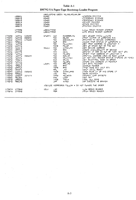
1730el0 17311104 173010 11'3"14 173016 1731/12" 173022 17302" 173e26 17303£1 17;,;:,32 t73~.36
1730 4 " 173,,42 173,,44 1731346 17'31/l~21 173;!52 173e54 173~621 ~ 73Z62
~7'3a66 17301" 173072 173014 173076 (j000~1 J00212'2 7001Z1:.::3 .:0Z0~~41 ,)000<16 J0QHP7 1715'0 177560 ,112701 ~127~2 ,I12n3 1105012 ,'U742 1121H6 :1413['4 l05714 100175
"1" 7 12 :'127:'0
:l,~4 41
[image:30.614.69.543.55.753.2]'4~6'\1 ,1'1('1111 :111;:'2 '1052141 11215714 103376 116"12 ~0'211 123221 "£11366 105222 ~00142 1715621 171550 'l.60iOIH': "'0121006 173100 Table A-I
BM792-YA Paper-Tape Bootstrap Loader Program
'Rt:GISTE~S Rl-"1 R2."2 R3-"3 Fl4d4 SP~"6
flC.'"
HSRII1775~0 l.SR·1715~0SHIHI "IOV "'OV
MOV
CI,..
"IOV "'0"8
DEVil
"'0"
TST RMt "Ov "'OV "'011 tqe MOVLO~PI MOV
INC TSTB fin ~OVB I~e eMf'£;! A~E I~CB JMP #16001110,Rl,
'~., R2 'OEV.~,R"5 ,R2 PIf,-(I'(2) PC,sP _(R3),R'l l'H4 DE-Vi r-tt,'R~ IiIZ4,S,",
R4, .. (1«1)
SP,R1 Fq,,"R~ 9Rl,Ril IIH(4 lIH4 ,-2 2IR4),_H2 "'Hi R2,'3~' ,-OOP (H2)'" .IR21
,A~CqESS POI~TER
,TrMPORARV STORAGE
,TfMPORAkV STORAGE IOnICr;' POI~tER
,S HCK PO I'JTER ,PQOr:RAM COUNTER
'~J~W SPlED READER A1DRESS
'L~W SPEEO REAOE~ ADDRES~
ISET ~EMORV ~HECK '-l~ITS tT~Ap VEC'OR IS ~O~ T ON 'lIb
,p~t~TrR TO OEvlCE AJD~ESSES
ICLEAR THAP STATUS AT ~O~A'l~N
,SET
TRAP ADD~~SS IN LOCATtO~ 4IS£T U~ STACK OUT
or
T~E ~'YIGfT DEVIC~ ADDRESS
IC~tCK AVAILABll,.lTY
or
DEVICE,BPA"CI-I IF' f.lSR IS OUT ~r TAPf IBIT ~~)
IRrsrT T4AP ADDRESS AT ~OC'T!ON 4
ISPE~IAL ADDHESS U~ED AS MAS~ ~ATl~
'D~ ME~ CHKI READER STATUS A~DRES5 15 ~OV(~
,5fT RiaX7752, MASK IN S.'~4
,5 TOQE OWN AODRESS I~ POtNTlQ ,GFT BYTE POINTE~
,ENAFIL.E
HEADF.R-ITr~T DONE BIT (BIT 071
IWAI· VNTI~ qEADY
IT~EN 'lCK IT UP A~D 5TOQE IT
,BUMP P01NTE~
JSTOQE~ JU"IP OFFSET?
I NOT Vf:T
J HS, Al.L. OO'IJ[
IG~ EXECUTE AS BRA~CH
'I,.Ow S~EtO RtAOER
APPENDIX B
BM792-YB BULK STORAGE BOOTSTRAP LOADER
The BM792-YB ROM is shipped with jumper wires connected for address group 773100-773 176, and its diode matrix ispreprogrammed for a bulk storage (disk or DECtape) bootstrap loader program. The BM792-YB is used in a PDP-l I Systeril that has at least 4K of read-write memory and one or more mass storage devices, such as disk or DECtape.
The actual bootstrap loader program, stored in the first 256 words of a disk or DECtape, is transferred from the device into rcad-write memory by the BM792-YB program. The transfer is started from location 0 of the device. and the loaded routine is assumed to be operative at read-write memory location O. The BM79:!-YB program
jumps to location 0 after a satisfactory completion of the transfer, so that there is automatic starting of the actual bootstrap loader program. If error conditions occur during the running of the BM792-YB program. the program starts over again.
The sequence of operations used by the bulk storage bootstrap loader is as follows:
I.
3.
4.
5.
6.
It lktermines whether the device is a disk or DECtape from the address set in the SWITCH REGISTER.
If the device is a DECtape transport, it moves the tape until the front endzone is sensed.
It rcads 256 words stored in the device, starting with address 0 of the device.
The loader then stores the 256 words in read-write memory sequential locations, starting with location O.
The loader checks for errors and starts the program over if any errors occur.
The loader then jumps to read-write memory location 0 for automatic starting of the actual bootstrap loader program.
A program listing for the bulk storage bootstrap loader is provided in Table B-1. Hardware addresses in the PDP-II
usc 18 bits: thus. bits A 15. A 16. and AI 7 are considered in designating the most significant octal digit of the ad-dress. 'The software assembler uses 16-bit addresses; consequently, only bit A I 5 is used to designate the most
sig-nificant octal digit of the address. Therefore, the addresses in Table B-1 arc listed as I 73XXX instead of 773XXX.
The operating procedure for use of the BM792-YB bulk storage bootstrap loader is as follows:
Step Procedure
Set the HALT/ENABLE switch to HALT, then to ENABLE.
2 Set the ROM address, 773 I 00, into the SWITCH REGISTER.
3 Depress the LOAD ADDR switch.
Step 4 5 173108 173104 113186 173110 173114 173120 173122 173126 173130 173132 173134 173 I 36 173140 173144 t73U6 173150 173152 173154 173156 BEGIN START Procedure
Set the address of the word count register of the disk or DECtape to be used into the SWITCH REGISTER. Th,e standard addresses for the word count registers of the DEC devices are as follows:
RCl] Disk RFl] Disk RK] I Disk RPl] Disk TC 1] DECtape
777450
777462
777406
776716
777344
[image:32.626.13.549.59.756.2]Depress the START switch. The disk or DECtape data should then read into the read-write memory.
Table B-1
BM792-YB Bulk Storage Bootstrap Loader Program
J REGISTER ASSIGNMENTS: 000000 R0=10
000001 Rlall
013701 177570 000005- BEGIN: 010100 0.12710 177400' 020027 1773~4 001007 012740 004002 005710 100376 00574e 100363 022020 012740 START. 000005 105710 100376 005710 100754 105010 000137 000000 000001 000004R 000040R MOV RESET MOV MOV CMP BNE MOV TST BPL TST BPL CMP MOV T3TB BPL TST BMI CLRB JMP .END U177570"RI RI"R0
#-256. ,,'R0
R0,,1I77344 START. 14002,,-(R0) IR0 • -2 ~(R0) BEGIN (R0)+,,(R0)+ IS,,-(R0> tR0 .-'2 'R0 BEGIN @K0 " 0
1<0 x%000000
=
000062k,READ SWITCH REG FOR ••••
'FORCE CLEAR IF RETRY ' •• ~.DEVICE WC ADDRESS JSET TO READ 256 WORDS
JlS IT DECTAPE?
INO. GO TO START
JYES. MOVE TAPE TO FRONT
'WAlT FOR ERROR 1
JIS IT ENDZONE? JNO. TRY AGA IN 'ADJUST POINTER 'NOW START ACTUAL READ
'WAIT FOR DONE
JERROR ENCOUNTERED?
JIF SO START OVER
JFOR OECTAPE"STOP TRANSPORT JGO TO ROUTINE LOADED
APPENDIX C
BM792-VC CARD READER BOOTSTRAP LOADER
The BM792-YC ROM is shipped with jumper wires connected for address group 773200-773276. Its diode ma trix is preprogrammed for loading binary data into the PDP-II memory from cards using the CR 1 1 or eM I I Card Reader. If tht' data represents a PDP-II program, the program can be automatically started upon
comple-tion of loading. The BM792-YC is used in PDP-II Systems that have at least 4K of read-write memory and a card reader.
On the card that is read, each pair of columns (column I and column 2; 3 and 4; etc.) beginning with column I contains two 8-bit bytes which represent one 16-bit word. Also a control bit can be contained in the second column of a pair. The eight bits that represent each byte are punched or marked in rows 2 through 9 of each column.
The first column of a pair contains the high-order byte (PDP-II bits 15-8) of the word and the second column of the pair contains the low-order byte (PDP-II bits 7.,.0) of the word. A control bit punched or marked in row
o
of the second column of a pair designates that the word in those two columns is a new Loading Address. Each Loading Address must be equal to zero modulo two because loading must begin at a word boundary in memory rather than a byte boundary. Loading is accomplished one word at a time, thus a new Loading Address can appear anywhere on the card. However, a Loading Address must be in the first two columns of the first card read.The absence of control bits in rows 12, II, I, and 0 of the second column of a pair designates the word as a Data Word to be loaded into the PDP-II memory. The Data Word can represent a machine instruction or data. After each Data Word is loaded into memory the current loading address is incremented by two.
A control bit in row I of the second column of a pair designates the word as a Transfer Address. When a Transfer Address is read, the bootstrap program issues a RESET and branches to the Transfer Address. The card which contains the Transfer Address passes through the card reader, but no other Loading Addresses or Data Words are read from it.
The operating procedure for use of the BM792-YC card reader bootstrap loader is as follows:
Step
2
3
4
5
6
7
Procedure
Set the HALT/ENABLE switch to HALT, then to ENABLE.
Load the input hopper of the card reader with the cards to be read.
On the card reader set the MODE switch to REMOTE.
On the card reader depn~ss the RESET switch and observe that the associated grel'n indicator lights. The card reader is now on-line.
Set the starting address, 773200, into the switch register.
Depress the LOAD ADDR switch.
Table C-l
BM792-YC Card Reader Bootstrap Loader Program
1
2 ;CR BOOTSTRAP
3
•
~ 73221" ,-1732005 ""'14""0 9P08:40'" 6 -:"~?~0 BIT09"1000
7 '4:'1002: B I Tl'h40000
8 "~t:'Il1:~0 R0="0 9 :"Jl'I~11I1 R1=U
a :-C?Je02 R2=%2
11 :'/1(11111113 R3="3
12 ~"'""0~4 R4="4
13 00Q1~"I7 PC="7
1 4 1771 60
1'5 CRS=177160 ICR STATUS REGISTER ADDRESS
RESET
16 1732110 :'~'~00!:> START: :C~EAR A~L PRESENT DEVICES
1.7 173202 '127~0 1771~e MOV *CRS.
FI"
:~OAD STATUS RECISTER 'DORESS18 1732('16 :1(102'1 MOV R0. Rl :MOVE TO Rl
19 17321'" -'3:?721 ";:1421~ fl! T *B!~08IBIT09,(R1)· : ~EST CR RUDY AND GET CRB ADDREIS
n l73214 ~ '1371 BNE START lAND WAtT 'OR REAOV, ON-\.IN£
<'1 !7~216 '" ~ 210 NEXTC: INC (iIIR0 lRUO A CUD
il2 17~22~ ":''1~'3 NEXTV: CLR R3 lCLEAR OAT' CONTENTS
23 :73,22 . ~~2ZIl1 CL.R Roll lAND COLUMN ;LAG
24 ~ 73224 "31Ql27 042l021~ TESTCD: BIT ~R0, nln.
liS CARD DONE 'L4C SET
~5 !7323e' {,c 13?;,1 BNE "JEXl(' IYES, READ A C'RO
'6 :73232 1157U WAITCI T5T8 GtRI1I
lIS COLUMN READY 'LAG lET
?7 173234 1;}:l373 QPL TESTCD
INO, WAIT ,OR COLUMN AND/D~ CAIIIO DONE
'6 :.73236 ,""1<'3:"3 SWA8 R3 I~EARRANGE THINGS
29 173240 151111:3 91S8 (iIIR1, R3
lAND GET THIS COLuMN
l~ 173242 "'O;l~4 COM Roll liS THIS SECONO COLUMN or 'AIR
11 ~7't244 1:H772 8MI WA PC 1~IRST, GET ANOT~EIII
,'2 17,3246 121?!>1 0,"002'1 CMP8 ~PC, leRl)
ITEST HIGH BYTE 0' CRB
~3 i732~2 ~:::142'5 BEQ TRA~SF IROW 1 IS TRANlrtR 'LAG
~4 173254 "~:30Z2 BCT DATA IROW ",1-e IMPLIES DnA
~5 173256 "l;'3~2 MOV R3. RI! :OTHERWISE Rowell 1"'1'1.1£1 LOAD ADO
~6 17321>e ,~ :!'~7'57 8R NEXTV lAND START NEW PAIR
"7 173262 :"1"1322 ,)ATAI t-IQV R3. (R2). ISTORE DATA 'WOAD
~8 173264 n0755 8R NEXTV lAND GET NEW COLUMN PAIR
~9 173266 ,~31e'27 0401:)"0 TRANSF": aIT taR0, 'BIT1. IWAIT 'OR CARD DONE
.""
173272 r.:-:1175 8EQ TRAt-./H lIN A TIGHT LOOP41 173274 i'Me05 RESET ITHEN CLEA~ CR 'LAGS
42 173276 ,l:?'J113 JMP (ltR3 lAND TRANS'ER TO LOADED PROGRAM
43 "(l"lI1'U .ENO
f1IT~o 0i.:04~0
E' IT~9 001030 8IT1' 0400210
CRS 177160
':lAT. 173262
"JElCTC 173216 "EliTV 173220 PC 0"00217 R
Q1 0~00210R
Rl 0~11I0hR
"2 0k:11I01l2 R
D3 3C00Z3R
i::4 01:00Z4 R
!,'TART 1732~0
TE"TCO 173224
TRAN~F' 1732~6