International Journal of Emerging Technology and Advanced Engineering
Website: www.ijetae.com (ISSN 2250-2459, ISO 9001:2008 Certified Journal, Volume 9, Issue 1, January 2019)
35
Realization of MIN-MAX Circuit for Rule Base Block of Fuzzy
Logic Temperature Controller using P-Spice Simulator
Srismrita Basu
1, Subhodip Maulik
21,2Institute of Engineering and Management
Abstract— This paper proposes the realization of a CMOS min–max circuit for the Rule-Base block of Fuzzy Logic Temperature controller using P-SPICE. Here, we mainly deal with the analog implementation of VLSI circuit. Then digital implementation was compared with analog implementation and the advantages of the analog implementation for this particular case were presented. Popularity of the analog implementation is due to the fact of their continuous-time-processing and high frequency and low power implementation.
Keywords— Fuzzy logic, analog implementation, digital implementation, current mode, current mirror, bounded difference.
I. INTRODUCTION
A mathematical system that takes continuous values between zero and one, in contrast to classical or digital logic, which operates on discrete values of either zero or one, and analyzes analog input values in terms of Fuzzy variables is called Fuzzy logic. In a 1965 paper by Lotfi A, Zadeh of the UC Berkeley, fuzzy logic was first introduced. In another paper in 1973, it was elaborated when concept of Fuzzy set was introduced. For our particular work, we have used Takagi-Sugenos type controller where we are concerned majorly with the Rule Base block in which a set of rules specifying the combination of input membership values are stored. Application to multi-input-multi-output problems and single- input- single-output problems are possible because the controllers use the inference mechanism.
The block diagram of Fuzzy controller is shown in fig-1.
Fig-1 Block diagram of Fuzzy logic controller
To design the Rule base block we consider the analog implementation of CMOS over digital implementation.
II. DIGITAL IMPLEMENTATION
International Journal of Emerging Technology and Advanced Engineering
Website: www.ijetae.com (ISSN 2250-2459, ISO 9001:2008 Certified Journal, Volume 9, Issue 1, January 2019)
36 Binary data are easily saved which allows multistage fuzzy processing. However, to obtain accurate and fast processing, the corresponding Fuzzy vectors and parallel structures are required. Digital implementation of basic Fuzzy operation leads to complicated and huge VLSI circuits. The density and speed of these circuits are continuously increasing with advancement in technology to be able to implement much efficient Fuzzy logic systems.
Digital Fuzzy processors are designed for flexible applications. Digital Fuzzy processors therefore must implement a considerable number various Fuzzy operators, inference rule, and membership functions. Provided appropriate programming is possible, the Fuzzy operators make the Fuzzy processors efficient for a large range of applications. Now, linguistic rules derived from a human
expert combined with appropriate programming
environment, can be directly translated into the implementation on a chip. Digital implementation is used in robots, expert systems, diagnosis control, image recognitions etc.
III. ANALOG IMPLEMENTATION
Analog circuits have several advantages over the digital ones, namely power dissipation, the speed of processing, and functional density. They are capable of performing continuous time processing and are flexible enough to be compatible with actuators, sensors, and other types of analog signals. Hence they are able to deal with analog Fuzzy values. By dealing with transistor characteristics, non-linear Fuzzy operations and membership functions can be easily synthesized. Provided that no specific digital signal processing is required, A/D or D/A converters are not necessary when implemented in a real system. For some applications requiring low-consumption, low-cost, compact and high-speed stand-alone chips, digital controllers can be replaced by analog circuits. The absence of reliable memory cells is the only issue here. They are generally not suited for pipeline structures with limited programmability opportunities. However, the nature of Fuzzy variable systems requires extensive parallelism which makes analog circuits suitable for limiting the problem of error accumulation.
Analog implementation is used in stable and low-noise analog technologies (n-well CMOS, Bi-CMOS) having sufficient accuracy with wide frequency range. Analog implementation consists of two mode of operations- 1) Voltage Mode and 2) Current Mode
III.1 Voltage Mode
Voltage mode makes it easy to distribute a signal in various parts of a circuit. Voltage mode can easily implement non-linear operators such as the MIN, MAX and truncation. Emitter coupled Fuzzy logic gates are circuits which are devised by Multi-input MIN & MAX circuits. The non-linear gates present good characteristics and robustness. Such circuits that cause an acceptable error associated with the transition region in which multiple devices are active, are impractical with MOS transistors. CMOS multi-input MIN-MAX circuits using gain-enhanced voltage followers based on differential amplifiers have great frequency and accurate performance but are more complicated.
In voltage-mode Fuzzy circuit, large energy is stored into the parasitic capacitances and speed is limited by charging delays of various capacitors. They suffer from lack of precision as signals are sensitive to changes in supply voltages. The problems occur because several functions are very difficult to build in voltage-mode and also due to the sizing of some components. To achieve additions and to convert voltages into currents, this type of implementation needs resistors. But, the integrated resistors involved are generally inaccurate, cumbersome and involve significant parasitic capacitances. Parallelism of the Inference engine (especially when the number and size of output sets is large) generates a serious problem of
de-Fuzzification. This approach causes high-power
dissipation, increase in chip area and high cost. These problems can be removed by the Current mode operation.
III.2 Current Mode
These circuits can achieve summation and subtraction in the simplest way of wire connections and do not require resistors. This leads to configurations, which exhibits high speed and great functional density. They are used by systems requiring a high level of interconnectivity.
The main advantages of the current mode circuit are- (i) Low power dissipation
(ii) Good insensitivity to the supply voltage fluctuation (iii) Low supply voltage
Since, current mode circuits have a single fan-out, the distribution of signals requires multi-output current mirrors.
III.2.1 Current Mirror
International Journal of Emerging Technology and Advanced Engineering
Website: www.ijetae.com (ISSN 2250-2459, ISO 9001:2008 Certified Journal, Volume 9, Issue 1, January 2019)
37 An ideal current mirror is an ideal current amplifier. There are 3 main specifications to a current mirror-(a) The current level it produces, (b) The minimum voltage drops the mirror necessary to make it work properly, and (c) Its ac output resistance which determines how much the output current varies with the voltage applied to the mirror.
The n-channel MOSFET current mirror with a resistor to set the reference current IREF is shown in fig.2.
Fig-2 n-channel MOSFET Current Mirror
In modern research, the transistors are replaced by the MOSFET to develop the current mirror as the speed of MOSFET is much higher and the power dissipation is low. A basic realization of multiple-output CMOS current mirror is shown below in fig-3.
Fig-3 Basic n-output CMOS current mirror
Since each output current is slightly modulated by output voltage throughout the early conductance, therefore the circuit is however not suitable for synthesizing accurate functions. The output current should be independent of the output voltage, which is obtained by reducing the conductance as for the 3 common mirrors shown in fig-3. The output voltage of the circuit is then independent of the drain voltage of the transistor which imposes the current.
Wilson mirrors, because they require a single polarization voltage instead of two superposed voltages, are often used in place of multi-output cascade mirrors as they are preferable for low power applications. The Mod-Wilson mirror is obtained by adding a transistor to the Wilson mirror to improve its symmetry. input current is well reproduced with perfectly matched identical transistors and provides good accuracy for this type of mirrors. The mirror accuracy depends on the matching of their transistors and their corresponding output resistance.
To synthesize Fuzzy logic operation, Current mirror can be used as building block. Hence, nine basic Fuzzy operations can be implemented on the ICs with standard CMOS technologies. The current mode exhibits good linearity which are not achieved in the voltage mode which in turn led to development of the Fuzzy integrated systems.
III.2.2 MIN-MAX circuit
The sentence connectives in any kind of Fuzzy controller is defined by the employment of Minimum (MIN) and Maximum (MAX) operators . In MAMDANI controller they also define the aggregation mechanism and the Fuzzy implication. Using membership functions, they are also used in the Fuzzification operation. The building block of these circuits is known as bounded difference circuit which is defined as
X Θ y={x-y; if x ≥ y
0; if x < y [where, x, y are two variables]
The combination of a current mirror and a diode fabricates the bounded difference circuit. The diode can easily be realized in the CMOS circuit by a single FET in which gate and drain is connected together.
International Journal of Emerging Technology and Advanced Engineering
Website: www.ijetae.com (ISSN 2250-2459, ISO 9001:2008 Certified Journal, Volume 9, Issue 1, January 2019)
[image:4.612.323.568.158.385.2]38 Input and output of Bounded difference circuit is given below in fig-5.
Fig-5 Input and output of Bounded difference circuit
Now, Fuzzy circuits can be designed only by specifying connections between different sub-circuits, as bounded difference and algebraic sum are sufficient to realize all Fuzzy functions.
MIN function of two inputs x and y can be derived by using bounded difference operator as follows:
MIN (x, y) = x Θ (x Θ y).
The two input MIN circuit is given below in fig-6.
Fig-6 A two input MIN circuit
[image:4.612.50.289.163.379.2]The input and output of MIN circuit is given below in figure 7.
Fig-7 Input and output of MIN circuit
MAX function of two inputs x and y can be derived by using bounded difference operator and Add (+) operator as follows:
MAX (x, y) =(x Θ y) + y
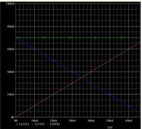
The two input MAX circuit is given in fig-8.
Fig-8 A two input MAX circuit
[image:4.612.325.569.474.663.2] [image:4.612.52.288.487.695.2]International Journal of Emerging Technology and Advanced Engineering
Website: www.ijetae.com (ISSN 2250-2459, ISO 9001:2008 Certified Journal, Volume 9, Issue 1, January 2019)
39
Fig-9 Input and output of MAX circuit
IV. CONCLUSION
An attempt has been made here to initiate work on analog realization of fuzzy circuits, but the implementation involves a large number of MIN-MAX circuits, which is time consuming. Research and development is also continuing on fuzzy applications in software, as opposed to firmware, design, including fuzzy expert systems and integration of fuzzy logic with neural network and so called adaptive “genetic” software systems, with the ultimate goal of building “self-learning” fuzzy control systems.
REFERENCES
[1] Rajasekaran, Sanguthevar, and GA Vijayalakshmi Pai. Neural networks, fuzzy logic and genetic algorithm: synthesis and applications (with cd). PHI Learning Pvt. Ltd., 2003.
[2] Design of Fuzzy Controllers:
http://faculty.petra.ac.id/resmana/private/fuzzy/design.pdf
[3] Fuzzy control system:
http://en.wikipedia.org/wiki/Fuzzy_control_system
[4] Current Mirror: http://en.wikiepedia.org/wiki/Current_mirror [5] Razavi, Behzad. Design of analog CMOS integrated circuits. 2005. [6] Fuzzy Logic:
http://faculty.petra.ac.id/resmana/private/matlab-help/pdf_doc/fuzzy/fuzzy_tb.pdf
[7] MIN and MAX Circuit:
http://portal.acm.org/citation.cfm?id=79828.79833
[8] Jacob, R., Harry W. Li, and David E. Boyce. "CMOS circuit design, layout, and simulation." IEEE Press Series on Microelectronics Systems (1998): 355-361.
[9] Maulik, Subhodip. "Realization of low cost bluetooth based visual sensor node for pest and disease detection in crops." International Journal of Emerging Technology and Advanced Engineering 2, no. 6 (2012).
[10] Basu, Srismrita. "Realization of fuzzy logic temperature controller." International Journal of Emerging Technology and Advanced Engineering 2, no. 6 (2012).
[11] Maulik, Subhodip, and Srismrita Basu. "Comparative Study of Adaptive Filter and Notch Filter for Filtering of Corrupted Signals." [12] Maulik, Subhodip, Srismrita Basu, and Theda Daniels-Race.
"Electrospray-assisted carbon nano tube deposition on aluminum without a binding agent." Bulletin of the American Physical Society 61 (2016).
[13] Maulik, Subhodip, Srismrita Basu, Hsuan-Chao Hou, and Theda Daniels-Race. "Voltage-Controlled Deposition of Dispersed Carbon Nanotubes onto a Conducting Substrate Without a Catalyst." Advanced Science, Engineering and Medicine 10, no. 6 (2018): 564-567.
[14] Maulik, Subhodip, Anirban Sarkar, Srismrita Basu, and Theda Daniels-Race. "Voltage-Controlled Spray Deposition of Multiwalled Carbon Nanotubes on Semiconducting and Insulating Substrates." Journal of Electronic Materials (2018): 1-6.
[15] Maulik, Subhodip. "Voltage-Controlled Deposition of Nanoparticles for Next Generation Electronic Materials." (2018).
[16] Basu, Srismrita, Subhodip Maulik, Hsuan-Chao Hou, Theda Daniels-Race, and Martin Feldman. "Surface enhanced Raman spectroscopic substrate utilizing gold nanoparticles on carbon nanotubes." Journal of Applied Physics 122, no. 17 (2017): 175107. [17] Basu, Srismrita. "Surface Enhanced Raman Scattering (SERS)
Substrates and Probes." (2017).
[18] Basu, Srismrita, Hsuan-Chao Hou, Debsmita Biswas, Subhodip Maulik, Theda Daniels-Race, Mandi Lopez, Michael Mathis, and Martin Feldman. "A needle probe to detect surface enhanced Raman scattering (SERS) within solid specimen." Review of Scientific Instruments 88, no. 2 (2017): 023107.
[19] Hou, Hsuan-Chao, Yaser Mohammadi Banadaki, Srismrita Basu, Subhodip Maulik, Shu-Wei Yang, Safura Sharifi, Martin Feldman et al. "Characterization of Sputtered Nano-Au Layer Deposition on Silicon Wafer." International Journal of Advanced Research Trends in Engineering and Technology 3, no. 12 (2017).
[20] Maulik, Subhodip, Srismrita Basu, and Theda Daniels-Race. "Dispersed Molybdenum Disulfide Deposition onto a Conducting Substrate Using a Voltage Controlled Deposition Technique." Advanced Science, Engineering and Medicine 10, no. 12 (2018): 1224-1226.
[21] Hou, Hsuan-Chao, Yaser M. Banadaki, Srismrita Basu, and Safura Sharifi. "A Cost-Efficient Surface Enhanced Raman Spectroscopy (SERS) Molecular Detection Technique for Clinical Applications." Journal of Electronic Materials (2018): 1-8.
[22] Basu, Srismrita, HsuanChao Hou, Debsmita Biswas, Theda Daniels-Race, Mandi Lopez, J. Michael Mathis, and Martin Feldman. "Single fiber surface enhanced Raman scattering probe." Journal of Vacuum Science & Technology B, Nanotechnology and Microelectronics: Materials, Processing, Measurement, and Phenomena 35, no. 6 (2017): 06GF01.