Frequency upconversion in nonpolar a
plane GaN/AlGaN based multiple
quantum wells optimized for applications
with silicon solar cells
Radosavljević, S, Radovanović, J, Milanović, V and Tomic, S
http://dx.doi.org/10.1063/1.4890029
Title
Frequency upconversion in nonpolar aplane GaN/AlGaN based multiple
quantum wells optimized for applications with silicon solar cells
Authors
Radosavljević, S, Radovanović, J, Milanović, V and Tomic, S
Type
Article
URL
This version is available at: http://usir.salford.ac.uk/37360/
Published Date
2014
USIR is a digital collection of the research output of the University of Salford. Where copyright
permits, full text material held in the repository is made freely available online and can be read,
downloaded and copied for noncommercial private study or research purposes. Please check the
manuscript for any further copyright restrictions.
Frequency up-conversion in nonpolar a-plane GaN/AlGaN based multiple quantum
wells optimized for applications with silicon solar cells
S. Radosavljevi, J. Radovanovi, V. Milanovi, and S. Tomi
Citation: Journal of Applied Physics 116, 033703 (2014); doi: 10.1063/1.4890029
View online: http://dx.doi.org/10.1063/1.4890029
View Table of Contents: http://scitation.aip.org/content/aip/journal/jap/116/3?ver=pdfcov
Published by the AIP Publishing
Articles you may be interested in
Optimization of InAs/AlInAs quantum wells based up-converter for silicon solar cells J. Appl. Phys. 110, 063713 (2011); 10.1063/1.3641977
Ultrafast intersubband relaxation and nonlinear susceptibility at 1.55 m in GaN/AlN multiple-quantum wells Appl. Phys. Lett. 84, 1102 (2004); 10.1063/1.1647275
Well-width dependence of photoluminescence emission from a-plane GaN/AlGaN multiple quantum wells Appl. Phys. Lett. 84, 496 (2004); 10.1063/1.1638884
GaN/AlGaN multiple quantum wells on a-plane GaN pillars for stripe-geometry nonpolar ultraviolet light-emitting devices
Appl. Phys. Lett. 83, 2599 (2003); 10.1063/1.1614835
Frequency up-conversion in nonpolar a-plane GaN/AlGaN based multiple
quantum wells optimized for applications with silicon solar cells
S. Radosavljevic´,1J. Radovanovic´,1,a)V. Milanovic´,1and S. Tomic´2
1
School of Electrical Engineering, University of Belgrade, Bulevar kralja Aleksandra 73, 11200 Belgrade, Serbia
2
Joule Physics Laboratory, School of Computing, Science and Engineering, University of Salford, Manchester M5 4WT, United Kingdom
(Received 4 June 2014; accepted 1 July 2014; published online 17 July 2014)
We have described a method for structural parameters optimization of GaN/AlGaN multiple quantum well based up-converter for silicon solar cells. It involves a systematic tuning of indivi-dual step quantum wells by use of the genetic algorithm for global optimization. In quantum well structures, the up-conversion process can be achieved by utilizing nonlinear optical effects based on intersubband transitions. Both single and double step quantum wells have been tested in order to maximize the second order susceptibility derived from the density matrix formalism. The results obtained for single step wells proved slightly better and have been further pursued to obtain a more complex design, optimized for conversion of an entire range of incident photon energies.
VC 2014 AIP Publishing LLC. [http://dx.doi.org/10.1063/1.4890029]
I. INTRODUCTION
Ongoing development of novel device concepts, materi-als, and fabrication processes is aimed at lowering the cost of solar power and hence at making it more competitive.1–5 Significant research efforts are directed towards enhancing the performance of solar cells (SCs), as well as towards opti-mizing their fabrication and installation and improving their working efficiencies.6The overall energy conversion capabil-ity of SCs has increased steadily in the last decade through enhanced photon absorption and charge carrier transport. The highest share in production and market belongs to solar cells based on silicon, both in crystalline and polycrystalline form due to its low price and availability, as well as the maturity of crystal growth and fabrication processes. Yet, like other sin-gle junction/sinsin-gle bandgap devices, they suffer from rela-tively weak conversion efficiency due to the wavelength mismatch between the narrow wavelength band associated with the semiconductor energy gap and the broad band of the (blackbody) emission curve of the Sun. The power loss is associated with both long-wavelength photons that do not have enough energy to excite electron–hole pairs across the energy gap (leading to a 20% loss in silicon) and short-wavelength photons that excite pairs with energy above the gap, which thereby waste the extra kinetic energy as heat.
Recently, nanoengineering approaches to enhance solar power conversion efficiency have started to receive consider-able interest.4,5,7Within such methods, sub-bandgap photons (that would normally be transmitted straight through the SC) may be utilized in a process called up-conversion (UC) to produce an above-bandgap photon,5,7–9or, on the other hand, above-bandgap photons can be reduced to multiple lower energy photons in a process called down-conversion (DC). Using one or both of these processes can increase the current collected in a solar cell. One of the unique advantages of this
concept is that it is compatible with many existing solar tech-nologies, due to the fact that only the incoming solar spec-trum is modified. For example, the UC layer can be attached to the rear of a bifacial solar cell without disturbing the per-formance of the device for the above bandgap photons.9 Consequently, any additional photocurrent that is generated via the UC results in performance enhancement. In addition, it is also possible to place a reflector behind the UC layer so that no luminescence escapes out of the rear of the device.
Semiconductor quantum well (QW) heterostructures offers extra degree of freedom in designing the optically active transitions between quantum states in such nanostruc-tures. By following the quantum engineering paradigm in the materials modeling, by suitable variation of semiconductor QW width, potential height of surrounding barrier material and shape of the QW itself, it is possible to tune the optically active transitions in such nanostructures to match simultane-ously the wavelength of the incident light and the desired wavelength of output signal to the absorption spectra of bulk solar cell device. Moreover, by placing them in a QW array in which each of the quantum wells is with slightly different absorbing wavelengths and each of them with the exactly the same output wavelength, potentially it would be possible to achieve the broadband absorption of the sunlight with nar-row output emission form such device. Another possible advantage of the up/down convertor based on the QW struc-tures when compare to doped material is in much more suppressed detrimental Shockley-Hall-Read nonradiative recombination too. Potential advantage of QW based up (or down) converters when attached to the bulk based absorption region of the conventional solar cell, are also in the fact that they can convert the part of the sun spectra otherwise trans-parent (or with energy lost in the form of heath) in the single energy gap absorption region SC design without converter, for the benefit of increased efficiency of such SC design.
In order to overcome the loss of low-energy photons, we have considered a model of up-converter based on nonlinear
a)E-mail: [email protected]
0021-8979/2014/116(3)/033703/6/$30.00 116, 033703-1 VC2014 AIP Publishing LLC
optical effects related to intersubband transitions in quantum well structures. Nonlinear optical effect involves a couple of photons unusable by the solar cell, whose sum of energies is almost equal to the value of the bandgap (Eg) of silicon. After conversion, a high-energy photon (emitted via the tran-sition of excited electron down to the ground state of the quantum well) can be reused by the SC. Thus, the larger por-tion of the solar spectrum may be exploited and the effi-ciency of current generation would increase.
We started by designing individual one-step QWs through varying their structural parameters (the widths of step and well layers and the Al content in the step region) in order to influence the positions of bound states and the shape of the corresponding wavefunctions. The goal was to optimize the light converter by searching for maximum of the relevant sec-ond order susceptibility derived from the density matrix for-malism. The best solution is determined by using the generic algorithm optimization tool for selecting the optimal parame-ters, subject to physical and technological constraints, thus en-abling us to obtain a realistic optimized quantum-well profile. In striving to benefit from larger off-diagonal matrix elements of wavefunctions of successive bound state-levels, we decided to reduce the electronic system and consider only the first three bound states to participate in the process.
A semiconductor that is to be used is such a nonlinear optical process needs to provide a large enough conduction band offset to accommodate at least three bound states. With respect to conditions listed here, we have chosen to use non-polar a-plane nitrides (AlGaN as a barrier and GaN as the well material), as it is the most suitable combination to our knowledge. Because of their wide direct bandgap, group III-nitrides and their alloys are the most promising materials for short-wavelength optical devices and are currently widely explored.10–13This procedure is repeated for various combinations of incident photon energies, to cover the whole sub-bandgap part of the spectrum. These individual quantum wells should be grown in a sequence, so to form a multi-QW structure capable of converting photons “continuously.” In more detail, adding a component (photon of a given energy<Eg) into the spectrum is consistent with adding a corresponding QW to the total design. The entire multi-QW structure comprises close to 50 subsequently grown GaN/ AlGaN QWs optimized for absorbing and converting pho-tons with different wavelengths.
II. THEORETICAL CONSIDERATIONS
The response of a material to the presence of electric field (E) of the incident radiation can be described by polar-ization (P)
P¼e0ðvð1Þ Eþvð2Þ
E2þvð3Þ
E3þ Þ; (1)
wherev represents the susceptibility of the material, while superscripts i in vðiÞ refer to the order of susceptibility. In this paper, we consider the second order nonlinear susceptibility
Pð2Þi ðxpþxqÞ ¼e0 X
j;k X
p;q
vð2ÞijkEjðxpÞEkðxqÞ; (2)
where indices i,j,k are Cartesian components of the field (x,y,z, subject to permutations).14All components contribute to nonlinear polarization effects, thus summation over all frequency combinations xp;q, need to be performed, while
their sum is fixed (xpþxq). Calculating the second-order
contribution within the perturbation theory, where the unper-turbed system is assumed not to be influenced by electric field, results in a well-known expression obtained from the density matrix formalism.14
We consider a multi-QW semiconductor structure, where the growth direction is labeled as z, therefore the second-order susceptibility amounts tovð2Þ
zzz, since thez
com-ponent of the dipole matrix element is significantly larger thanxandycomponents.15
In bulk semiconductor materials, as well as in semicon-ductor heterostructures, the scattering mechanisms exhibit considerable dependence on the wavevector and fre-quency.16–18 In case of “typical k” approximation this de-pendence in only frequency-related, while within “full k” approximation, it entails the wavevector relationship as well.16,17In the model of exact “full k” approximation, line-widths for all the transitions have very complex correlation with both the wavevector and frequency, clearly leading to different values for different transitions. In this paper, we use the averaged values of linewidthc, taking an equal value for all transitions, which leads to significant simplifications in the theoretical and numerical treatment of the problem considered here. We also assume that almost all electrons in the conduction band of the unperturbed system are in the ground state. All these assumptions are typically used in the literature and provide a good quantitative picture of the ana-lyzed problem. On the other hand, a very interesting treat-ment for obtaining the precise values of linewidths, offered in Refs.16–18is worth implementing and will be considered in future work.
In addition to the above considerations, we take into account only three relevant bound states of the QW, labelled 0, 1, and 2. Starting from the general expressions detailed in Ref. 14 (Eq. (3.6.18) therein), after introducing the above assumptions, we arrive to the expression for second-order nonlinear susceptibility in the form
vð Þzzz2 ¼e 3N
2h2l10l12l02Q; (3)
with
Q¼ 1
x10xp
ð Þ icþ
1
x10xq
ð Þ ic
" #
1
x20xpxq
ð Þ icþ
1
x21þxpþxq
ð Þ þic
" #
þ 1
x21þxp
ð Þ þicþ
1
x21þxq
ð Þ þic
" #
1
x21þxpþxq
ð Þ þicþ
1
x10þxpþxq
ð Þ þic
" #
:
Here, N is the electron number density, lnm¼ hnjzjmi are
the dipole matrix elements for transitions between states n andmof the QW (the relevant bound states are labelled 0, 1, and 2), xp and xq are the frequencies of incident photon
pairs. If we consider the cases close to resonance, where
xp¼x10þd and xq¼x21þe, with jdj x10 and jej x21, then the second summand in Eq. (4) becomes
much smaller than the first one, and Eq.(3)amounts to
vð Þzzz2 ¼ e 3N
2e0h2
l10l12l02
1
x20xpxq
ð Þ ic
1
x10xp
ð Þ icþ
1
x10xq
ð Þ ic
" #
; (5)
with the term½ðx21þxpþxqÞ þic1being neglected as well. The above expression can be further simplified to
vð Þ2 zzz ¼
e3N
2e0h2
l10l12l02
1
eþdþic
1
dþicþ
1
eDxþic
; (6)
whereDx¼x10x21. The absolute value of the real part of Eq.(6)is given by
Re vð Þzzz2
n o
¼ e
3
N 2e0h2
jl02l21l10j
dðDxeÞðdþeÞðdþeDxÞ þc22c2þðDxeÞðDxþdÞ ed
½ðeþdÞ2þc2d2þc2½ðeDxÞ2þc2 : (7)
On the other hand, if we take a strictly resonant case (xp¼x10,d¼0), then Eq.(7)reduces to
Re vð Þzzz2
n o
¼e
3
N
e0h2
jl10l12l02j
1þDxðDxeÞ
2c2
e2þc2
ð Þ 1þðDxeÞ 2
c2
!:
(8)
Our goal is to optimize the real part of the susceptibility in order to enhance the response of the material at frequency Eg=h(withEg being the energy bandgap of Si) which is best
absorbed by the silicon solar cell. Hence we start by setting
xpþxq¼Eg=hin Eq.(5). In order to successfully use the
Genetic Algorithm (GA) for global optimization,19–21as the tool for varying the QW parameters, we must formulate a suitable target function. GA is inspired by Darvin’s theory of evolution, i.e., it is modeled according to the idea of select-ing the fittest individuals in a current iteration of the algo-rithm and forwarding them to the next cycle to be used to create a new set of solutions, while less successful individu-als are dismissed. Starting from an initial set of solutions to the problem, analogous to survival of superior individuals in nature through generations, after a large number of itera-tions, GA returns the best solution within the search space that meets the predefined criteria. A current set of solutions which are considered during one iteration is called the popu-lation. The initial population can be either randomly gener-ated by the algorithm or preset, if there are indications where the optimum of the defined fitness (target) function should be searched for. The solutions from one population are used to form a new population (offsprings) which is expected to show progress compared to the individuals from previous
population, so called “parents.” Current parents are selected according to their fitness (target function value)—the more suitable they are, the more chances they have to reproduce, which is achieved by processes of crossover, mutation, and elitism. Crossover produces new individuals by directly recombining two parents to form an offspring, while muta-tions introduce certain changes in defining parameters of a promising parent. These changes are necessary in order to avoid converging towards local optima. In order to preserve the parents that are more suitable than offsprings in the cur-rent population, that would otherwise be lost after crossover and mutation, the term of elitism is brought in. One or more parents with top scores are considered elite members and are automatically transported to the next generation. This evolution-like iterative process is repeated until some condi-tion (for example, the total number of populacondi-tions or improvement of the best solution) is satisfied.
GA is usually implemented to process functions of the typefðx1;x2:::xi:::xnÞ, which depend on an arbitrary number
of independent variables: x1;x2:::xi:::xn. In this paper, GA is
used to find the best solution for the QW profile in terms of maximizing the second order susceptibility given by Eq.(6) (more precisely, the absolute value of its real part), so the fit-ness function may be defined as
F¼jRefv 2
ð Þ
zzzgj
Ne=e0
; (9)
wherejRefvð2Þ
zzzgjis given by Eq.(8).
III. RESULTS AND DISCUSSION
taken as pure nonpolar a-plane GaN, the barrier material is pure AlN (to provide a high enough potential barrier), while the step layer comprises AlxGa1xN. For calculating the
electronic states, we used a one band model that takes into consideration the effects of strain and band nonparabolic-ity.22,23In one-step quantum wells, the following input argu-ments are needed for evaluating the second order susceptibility: the widths of step and well layers and the con-tent of AlN in the step regions. GA algorithm needs to be supplied with realistic upper and lower boundaries for these parameters. In numerical calculations, we have used the fol-lowing values of additional parameters: mGaN ¼0:209m0,
mAlN ¼0:329m0 (where m0 is the free electron mass),10
EgAlN ¼6:47 eV,EgGaN¼3:24 eV,11 and the conduction to
valence band offset ratio is taken as 60:40.12The influence of strain is included by using parameters from Ref.10, so the outer barrier height amounts toUb¼1:76 eV. The relaxation
parameters in Eq.(5)are considered to be equal for all transi-tions and set to 5 meV which is a typical value used in the lit-erature, and the energy gap of Si is taken as 1.12 eV.
The first set of calculations was performed on one-step QWs, by using the genetic algorithm to find the best possible value of the fitness function(9), regardless of the individual photon energies xp, xq but fixing hðxpþxqÞ ¼1:12 eV.
The optimal QW profile obtained by this procedure has the total width equal to 2.27 nm, with the 1.22 nm wide step, and with step height of Us¼0:483 eV, as presented in Fig. 1.
These parameters yieldF¼1:351018cm3=V2, or jvð2Þ
zzzj ¼1:351018cm3=V2 ðeN=e0Þ.
In order to try to improve this result, the next run of the GA algorithm is performed for a modified quantum well encompassing two internal step layers. The extra potential step introduces two additional free parameters for optimiza-tion (its width and height), which should provide more free-dom in shaping the optimal profile. However, this did not lead to an increased values of the fitness function, and the reason is in the large energy separation between the ground and the second excited state (1.12 eV) required. Apparently, such separation can only be achieved in deep and narrow QWs and the insertion of additional step layer increases the well width (the minimal width of the second layer is limited to at least 0.8 nm to remain realizable). Fig.2
illustrates the profile of the optimized two-step QW compris-ing the followcompris-ing step-layers: one layer is 3.69 nm wide with the Al mole fraction of xS1 ¼0:81 and the other is 0.9 nm
wide withxS2¼0:19, while the total well width is 5.81 nm.
The corresponding value of the second order susceptibility (scaled by the ðeN=e0Þ constant) is 0:521018cm3=V2, which is clearly below the one-step QW result.
Having determined that the introduction of an additional step layer yields no improvement in the fitness function, we have returned to the one-step QW optimization, repeating the procedure for the almost complete sub-bandgap energy range with 10 meV increments in energy. In other words, the energy of one incident photon is varied in the (EgSi=2;Emax)
range, where Emax¼1:06 eV is the closest we could get to
EgSi and still obtain meaningful results. The energy of the
second photon is thus fixed atEgSihx, causing the
symme-try of the plot presented in Fig. 3, i.e., all the energies from the range ½EgSiEmax;Emax are encompassed. For each
[image:6.612.323.553.61.224.2]energy valuehx, we have performed the QW profile optimi-zation with respect to the fitness function (9). Individual QWs obtained by this procedure should form a sequence
[image:6.612.322.555.537.701.2]FIG. 1. The conduction band profile of the optimized single-step quantum well up-converter for Si solar cell.
FIG. 2. The optimized double-step quantum well profile.
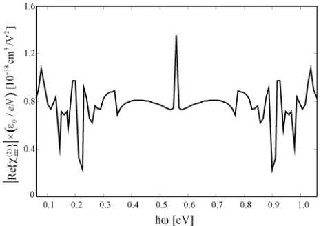
FIG. 3. The scaled value of the real part of the second order nonlinear opti-cal susceptibility as a function of the incident photon energy. Each point in this figure refers to the optimal result obtained for an individual quantum well within the multi-QW converter, optimized for a particular value of the incident photon energy (the energy of the second photon is evidently EgSihx).
[image:6.612.60.290.581.739.2](i.e., a multi-QW structure) capable of performing an almost continuous energy conversion of incoming radiation.
We observe that the parameters of individual QWs (such as step and well layer widths and the Al content in the step regions) can be tuned with high precision for a pair of photon energies. Photons with frequencies at the end of the spectrum determined by the silicon bandgap are more diffi-cult to accommodate as explained above. Furthermore, there is a narrow range of photon energies near the center (EgSi=2)
where the fitness function drops rapidly (Fig.3), due to spe-cific requirements for the QW profile that apparently cannot be best achieved with the chosen set of free parameters and the material system in question. One possibility is to allow for the variations of the outer barriers composition (AlGaN with high Al content rather than pure AlN), which may lead to an improvement of the target function, but complicate the overall multi-QW design.
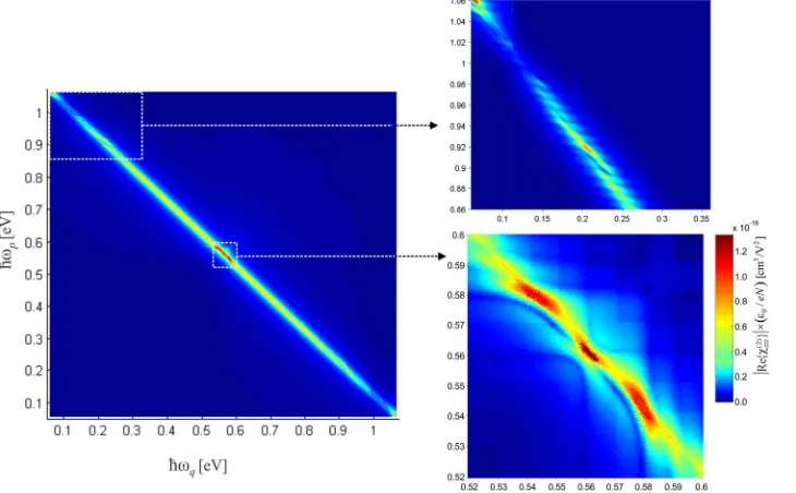
Finally, we have performed a set of calculations for the optimized sequence of QWs, taking into account nearly reso-nant photons according to Eq.(7), and varying the incident photon energieshxp andhxq. The obtained results are
pre-sented in Fig.4.
It is clear from the above figure, that only the points near the diagonal (very close to resonant conditions, with
e;d!0) have significant values, and the susceptibility drops rapidly as the sum ofhxp andhxq departs from Eg of
sili-con, for which the converter structure is constructed. The brown/red areas of Fig.4correspond to the highest values of the real part of susceptibility.
IV. CONCLUSION
Silicon is nowadays the most commercially used mate-rial for manufacturing solar cells; however, its energy gap significantly limits the spectrum of daylight that can be directly absorbed. Typical loss mechanisms include the transmission of sub-bandgap light and the thermalization of charge carriers generated by the absorption of photons with energies greater than the bandgap. Up-conversion of low
energy photons is a promising approach to reduce this por-tion of the losses, as an up-converter generates one high-energy photon out of two low-high-energy photons, which then creates free charge carriers in the solar cell. This was the focus of our paper, and the described procedure based on the use of genetic algorithm global optimization tool, allowed us to vary the structural parameters of nonpolar-nitride quantum wells in search of the best step QW profile, offering highest value of the relevant nonlinear susceptibility. The method was extended to obtain a multi quantum well up-converter structure which comprises a sequence of about 50 GaN/ AlGaN QWs, each optimized for conversion of photons with particular sub-bandgap energies. The a-plane non-polar nitride material system proved suitable for providing a large enough conduction band offset to accommodate three bound states with sufficient energy separation.
ACKNOWLEDGMENTS
This work was supported by the Ministry of Education, Science and Technological Development (Republic of Serbia), ev. no. III 45010 and NATO SfP Grant, ref. no. ISEG.EAP.SFPP 984068. S.T. wish to thank the Royal Society, London, grant “High Performance Computing in Modelling of Innovative Photo-Voltaic Devices” and Great Britain Sasakawa Foundation. We would like to thank Urs Aeberhard for useful discussions and suggestions.
1M. Green,Prog. Photovoltaics
9, 123 (2001).
2
R. R. King,Nat. Photonics2, 284 (2008).
3
S. Tomic´, T. S. Jones, and N. M. Harrison,Appl. Phys. Lett.93, 263105 (2008).
4T. Trupke, M. Green, and P. Wurfel,J. Appl. Phys.
92, 1668 (2002).
5
T. Trupke, M. Green, and P. Wurfel,J. Appl. Phys.92, 4117 (2002).
6
W. Shockley and H. J. Queisser,J. Appl. Phys.32, 510 (1961).
7N. Prodanovic´, J. Radovanovic´, V. Milanovic´, and S. Tomic´, J. Appl. Phys.110, 063713 (2011).
8
Y. Yi, L. Zhu, and Z. Shuai,Macromol. Theory Simul.17, 12 (2008).
9
[image:7.612.52.417.65.291.2]S. Fischer, J. C. Goldschmidt, P. L€oper, G. H. Bauer, R. Br€uggemann, K. Kr€amer, D. Biner, M. Hermle, and S. W. Glunz, J. Appl. Phys. 108, 044912 (2010).
FIG. 4. The scaled values of the real part of the second order nonlinear opti-cal susceptibility in a more general, non-resonant case, as a function of incident photon energies.
10S. Schulz, T. J. Badcock, M. A. Moram, P. Dawson, M. J. Kappers,
C. J. Humphreys, and E. P. O’Reilly, Phys. Rev. B 82, 125318 (2010).
11
P. Rinke, M. Winkelnkemper, A. Qteish, D. Bimberg, J. Neugebauer, and M. Scheffler,Phys. Rev. B77, 075202 (2008).
12T. J. Badcock, P. Dawson, M. J. Kappers, C. McAleese, J. L. Hollander,
C. F. Johnston, D. V. Sridhara Rao, A. M. Sanchez, and C. J. Humphreys,
J. Appl. Phys.105, 123112 (2009).
13S. Tomic´ and N. Vukmirovic´,Phys. Rev. B79, 245330 (2009).
14R. V. Boyd,Nonlinear Optics(Academic Press-Elsevier Science, 2003),
pp. 129–176.
15V. Milanovic´, Z. Ikonic´, and D. Tjapkin, Phys. Low-Dimens. Struct.7, 65
(1995).
16
T. Schmielau and M. Pereira,Phys. Status Solidi B246, 329 (2009).
17
T. Schmielau and M. Pereira,Microelectron. J.40, 869 (2009).
18T. Schmielau and M. Pereira,Appl. Phys. Lett.95, 231111 (2009). 19G. Goldoni and F. Rossi,Opt. Lett.
25, 1025 (2000).
20
A. Franceschetti and A. Zunger,Nature402, 60 (1999).
21
J. Radovanovic´, V. Milanovic´, Z. Ikonic´, and D. Indjin,J. Appl. Phys.99, 73905 (2006).
22S. Tomic´, A. G. Sunderland, and I. J. Bush,J. Mater. Chem.
16, 1963 (2006).
23