N A N O E X P R E S S
Open Access
The Extremely Enhanced Photocurrent
Response in Topological Insulator Nanosheets
with High Conductance
Shiu-Ming Huang
1*, Lin-Jie Lin
1, You-Jhih Yan
2, Shih-Hsun Yu
2, Mitch M. C. Chou
2,3,
Ho-Feng Hsieh
4, Chin-Jung Ho
4and Ruei-San Chen
4Abstract
The photocurrent was performed in topological insulator nanosheets with different conductances. The higher photocurrent is observed in the nanosheet with higher conductance. The responsivity is proportional to the
nanosheet conductance over two orders. The responsivity is independent of the light power intensity in vacuum, but responsivity drastically decreases at low power intensity in air. The ratio of the responsivity in air to that in vacuum is negatively proportional to the the inverse of the light power intensity. These behaviors are understood as the statistical photocurrent in a system with blocked molecules. The time constant decreases as the thickness increases. A longer time constant is observed in lower atmosphere pressure.
Keywords: Nanosheets, Photoresponse, Topological insulator
Introduction
It is an ongoing task to look for materials with higher photocurrent response. The short light penetration depth in solid-state materials leads to that the photocurrent response is dominated by surface carriers. A material with higher abundant surface carrier is a better candidate as a photodetector. For a long time, materials with high surface-to-volume ratios, such as nanowires, were widely studied [1–6]. Accompanied with the wide photodetec-tion bandwidth, low-dimensional materials with linear E-K dispersion, such as graphene, [7,8] graphene-based heterostructures, [1–4], two-dimensional transitional metal dichalcogenides (TMDs), and topological materials, have attracted wide attention [9–16].
The recent reports reveal that the reported photocurrent response varies in wide ranges [17–22]. One intuitively ascribes these distributions to different material growth and experimental conditions. Most of the reports focus their attention on the material component adjustment. The potential intrinsic mechanisms on these distributions
*Correspondence:smhuang@mail.nsysu.edu.tw
1Department of Physics, National Sun Yat-Sen University, 80424 Kaohsiung, Taiwan
Full list of author information is available at the end of the article
are less investigated and discussed. Clarifying the intrinsic mechanism might help one improve potential defect and greatly optimize the performance. It is believed that the sample quality should be a critical factor dominating the photocurrent response [17–22]. In addition to the crystal structure and component analysis, are there any other simple physical methods to determine the sample quality? It has come to our attention that the photoresponsivity distributes over a wide range with different sheet resistance based on a number of experi-mental reports. The transport processes of electron-hole pairs induced by photons follow scattering processes in mesoscopic solid-state systems, so the material conduc-tance would be a critical factor in dominating the reported photocurrent response. However, this effect is not yet well studied, and related experimental works are lacking.
To identify the conductance effect on the photocurrent response, we systematically investigated the photocur-rent response in topological insulator nanosheets with different conductivity. The photocurrent is linear with light power intensity, and the photocurrent is propor-tional to the dark current. The higher photocurrent is
Huanget al. Nanoscale Research Letters (2018) 13:371 Page 2 of 9
observed in the nanosheet with higher conductivity. The responsivity is proportional to the nanosheet conduc-tance over two orders. The responsivity is independent of the light power intensity in vacuum, but responsivity drastically decreases at low power intensity in air. The ratio of the responsivity in air to that in vacuum is neg-atively proportional to the the inverse of the light power intensity. These behaviors are understood as the statisti-cal photocurrent in a system with blocked molecules. The time constant decreases as the thickness increases. This behavior could be understood as the uniformity current flowing process. The charge and discharge time con-stants of different pressures are determined. A longer time constant is observed in lower atmosphere pressure. The responsivity,R, is linear with the nanosheet conductivity. The R at V = 0.1 V reaches 731 at nanosheets with higher conductance. These are higher than all reported values in (Sb, Bi)2(Te, Se)3 topological insulators and
low-dimensional materials and only lower than several reported heterostructures.
Experimental Method
Single crystals of Sb2Se2Te were grown by a homemade
resistance-heated floating zone furnace (RHFZ). The starting raw materials of Sb2Se2Te were mixed
accord-ing to the stoichiometric ratio. At first, the stoichiomet-ric mixtures of high-purity elements Sb (99.995%), Se (99.995%), and Te (99.995%) were melted at temperatures of 700∼800 °C for 20 h and then slowly cooled to room temperature in an evacuated quartz glass tube. The result-ing material was used as a feedresult-ing rod for the followresult-ing RHFZ experiment. After growth, the crystals were then furnace cooled to room temperature. The as-grown crys-tals were cleaved along the basal plane, producing a silvery shining mirror-like surface, and then prepared for fur-ther experiments. The Raman, EDS, and XPS spectrum support that the crystal is Sb2Se2Te. The X-ray
diffrac-tion shows sharp peaks that indicate that the Sb2Se2Te
crystal has high crystallinity and uniformity. Our previ-ous works show that physical parameters extracted from ARPES and the quantum SdH oscillation are consistent. These support the Sb2Se2Te crystal reveals high quality
and uniformity.
The Sb2Se2Te nanosheets were obtained by exfoliating
bulk crystals using dicing tape and were then dispersed on the insulating SiO2 (300nm)/n-Si templates with
pre-patterned Ti/Au circuits. Two platinum (Pt) metal contacts were subsequently deposited on the selected Sb2Se2Te nanosheets using focused-ion beam (FIB)
tech-nique. Figure 1a–c shows the SEM pictures of three Sb2Se2Te nanosheets. The thickness of nanosheets is
determined by atomic force microscopy, and measured thickness of three synthesized nanosheets were 58 nm, 178 nm, and 202 nm, respectively. The conductance of
these nanosheets were measured by Keithley 4200-SCS. The current were measured as a function of applied volt-age in a two-probe method. The I+and V+are the same contact point, and the I− and V− are the same con-tact point. To identify the intrinsic conductance effect on the photocurrent response, three nanosheets with dif-ferent conductance were prepared for the photocurrent measurement.
Results and Discussion
Figure1d–freveals a linear voltage-current relation. This indicates the metallic characteristic and the ohmic con-tacts between Pt electrodes and nanosheets. The mea-sured conductance,G, are 4×10⁻⁵, 0.006, and 7×10⁻⁵(S) for nanosheets with thicknesses of 202, 178, and 58 nm, respectively. The conductivity is higher than 1000 (S/m) which supports the extremely high crystal quality in our nanosheets.
Figure2a–cshows measured currents as a function of the light power intensity. Figure 2d–f reveals that the measured current is proportional to the light power inten-sity [27, 28]. The relation could be expressed as Ion =
βPα +Ioff, where theIon is the measured currents with
light, Ioff is the measured currents without light, β is
a constant related to the photocurrent response, P is the light power intensity, and α is a constant related to the light illumination condition between the devices and light. It is worth noting that the larger Ion is observed
in the nanosheet with largerIoff. The photocurrent, Iph,
is defined as Ion − Ioff. Table 1 lists the fitting result.
It shows that α ≈ 1 for all nanosheets with different thicknesses, and that supports the consistent optical char-acteristics in these nanosheets. It is worth noting that
β/Gis 1.1×10⁵±0.2×10⁵(A/WS) for all nanosheets. This indicates that the observed photocurrent is propor-tional to the effective conductance. This finding supports that aside from system geometry and the material band structure, the effective conductance of nanosheets would also be a critical factor dominating the photocurrent response.
TheIphoriginates from electron-hole pairs induced by
the interaction between injected photons and nanosheets. The induced electrons and holes flow in opposite direc-tions under applied electric bias. The effective Iph is
proportional to the applied voltage and the amount of electron-hole pairs. More injected photons lead to more electron-hole pairs. The light penetration depth is short and weak depending on the light power intensity. It is reported that the light penetration depth is roughly 20 nm in topological insulators which is smaller than the thick-ness of our nanosheets [23,24]. TheIph should be
Fig. 1 a,b, andcshow the SEM pictures of three Sb2Se2Te nanosheets. The nanosheet thickness is measured by AFM. Two Pt contacts were deposited on a nanosheet to measure the photocurrent.d,e, andfreveal the voltage-current relation, and it is linear. That indicates the ohmic contact between the Pt electrodes and Sb2Se2Te nanosheets
Iph spreads over a two-order difference. Apart from
the effective induced electron-hole pairs, the observed different Iph should originate from intrinsic properties.
In order to exclude extrinsic geometry effects on theIph
and quantitatively determine the performance of these nanosheets, the responsivity, R, is calculated using the following equation:
R= Iph
PS, (1)
where P and S are the light power intensity and the effective area, respectively.
Huanget al. Nanoscale Research Letters (2018) 13:371 Page 4 of 9
Fig. 2 a,b, andcshow the measured currents as a function of light power intensity in three samples with different thicknesses.d,e, andfreveal that the measured currents are proportional to the light power intensity. It comes to our attention that the largerIonis observed in the nanosheet with largerIoff
and not from the nanosheet geometry or experimental conditions.
As shown in Fig.1, the linear voltage-current relation supports that nanosheets reveal a metallic behavior. The light-induced electron-hole pairs would travel to two elec-trode contacts due to the applied voltage bias [27–29]. Following Ohm’s law, the related photocurrent could be determined through the relation Iph = VGwhere V is
the applied voltage bias between two electrodes. TheIph
is proportional to theG.
Figure4reveals theRas a function of theGin a log-log plot. The data points of Sb2Se2Te are the measured results
in this work, and data points of Sb2SeTe2 are extracted
from our previous work under the same crystal growth conditions and measurement setups [27]. The thickness of Sb2SeTe2 nanosheets are about 180 nm. The
[image:4.595.54.291.663.735.2]wave-length is 532 nm. Both Sb2Se2Te and Sb2SeTe2show that
Table 1Fitting parameters in Sb2Se2Te nanosheets
Thickness 202 nm 178 nm 58 nm
β(A/W) 5.5 641 6.7
Ioff(A) 6.67×10⁻⁶ 5.36×10⁻⁴ 3.80×10⁻⁶ β/G(A/WS) 1.37×10⁵ 1.06×10⁵ 0.96×10⁵
α 1 1 1
Ris independent of the light power intensity. These data points follow the tendency of the dot line over a wide range of the nanosheet conductance. This supports that Ris proportional to theG, which is consistent with our proposal.
A system with higher photocurrent response is greatly preferred for potential applications. As well as looking for new materials or systems with specific band struc-ture and band gap, a proper treatment on a system would be also suitable methods to enhance photoresponse. Our experimental results support that the intrinsic electric conductance would be a critical factor to optimize the photocurrent response. This might be achieved through appropriate growth conditions. As shown in Fig. 4, the photocurrent is 2 orders enhanced through conductance adjustment. This study could guide other researchers into constructing a suitable guideline in selecting a better sys-tem for further experimental studies through a simple electric test.
The R and detectivity at V = 0.1V reaches 731 and 2.6×10¹⁰at the nanosheet with higher conductivity. These photoresponses are larger than all reported values in (Sb, Bi)2(Te, Se)3topological insulators and low-dimensional
Fig. 3The responsivity of three Sb2Se2Te nanosheets. It reveals weak dependence of the light power intensity on responsivity. The higher responsivity is observed in the nanosheet with higher conductivity
comes to our attention that the reported conductivity in these low-dimensional materials are extremely high. This is consistent with our experimental result that the conductivity would be a critical factor dominating the photocurrent response.
Figure5depictsRas functions of the light power inten-sity in vacuum and atmosphere. It comes to our attention theRdrastically decreases when the light intensity is lower
than 500 Wm−2 in atmosphere. This supports that this
decreasing Rat low light intensity in atmosphere might come from the influence of the adsorbed molecular on the surface of our Sb2Se2Te nanosheet.
The photoresponse would be extremely sensitive to the condition of sample surface. In addition to the reduc-tion of the effective response area, surface defects and oxidation might reduce carrier mobility and lifetime.
[image:5.595.60.538.86.312.2] [image:5.595.59.540.489.703.2]Huanget al. Nanoscale Research Letters (2018) 13:371 Page 6 of 9
Fig. 5Responsivity and photoconductive gain as functions of the light power intensity at a wavelength of 532 nm. The responsivity is weak light power intensity dependence in vacuum. The responsivity decreases as the light power intensity decreases in atmosphere when the light power intensity is lower than 500W/m2
Recently, it is reported that adsorbed molecules on the surface of Bi2Se3 topological insulators bend the
struc-ture and lead to an additional 2DEG. This induced 2DEG would enhance the effective carrier mobility [30]. A sys-tem with higher carrier mobility might decrease the car-rier transit time and produce a higher photocurrent. On the other hand, the enhanced carrier mobility should be independent of the light power intensity. These sup-port that the observedRsuppression is mainly from the effective shining area, not from the intrinsic transport characteristics. Thus, it is believed that the drop ofRin air at low light power intensity should be more related to adsorbed molecular shadow effect than the intrinsic complex carrier relaxation effect.
The definition of the responsivity is the ratio of the induced carrier to the incident photons, and it also could be expressed asR = ηhfq, whereq,hf, andηare the car-rier charge, the photo energy, and the quantum efficiency, respectively. Theηis directly related to the material prop-erties and the light wavelength. To exclude other extrinsic and intrinsic effects and optimize the molecule shadow effect, theR(air)/R(vac)is plot as a function of the light power intensity. As shown in Fig.6, the ratio increases as power intensity increases and gradually saturates at high power intensity.
We propose a model that the incident photon number isY, themphotons interact with material, andnphotons are blockaded by adsorbed molecular on the surface. That
is,Y =m+n. TheZis the average induced photocurrent carrier number by one photon. In the extremely weak light intensity, the photo number is much less than the total molecular unit, the effective photocurrent should follow the statistical calculation, and the result supports that the quantum efficiency,η, could be expressed as
η(air)=
1− n 2Y
Z. (2)
This statically calculation supports that the effective photocurrent would be strongly related to the light power intensity in the limit of the weak light power intensity and long relaxation time; the photon number might be smaller than the “photo carrier creator.” The effective photocurrent could be expressed as
R(air) R(vac) ∝
1− n
2Y
(3)
[image:6.595.58.540.84.337.2]Fig. 6The ratio of the responsivity in air to that in vacuum as a function of the light power intensity. The data points go well with the theoretical predication. The inset shows the ratio of the responsivity in air to that in vacuum is negatively proportional to the the inverse of the light power intensity
power intensity and that indicates the surface covers with adsorbed molecules by 40%.
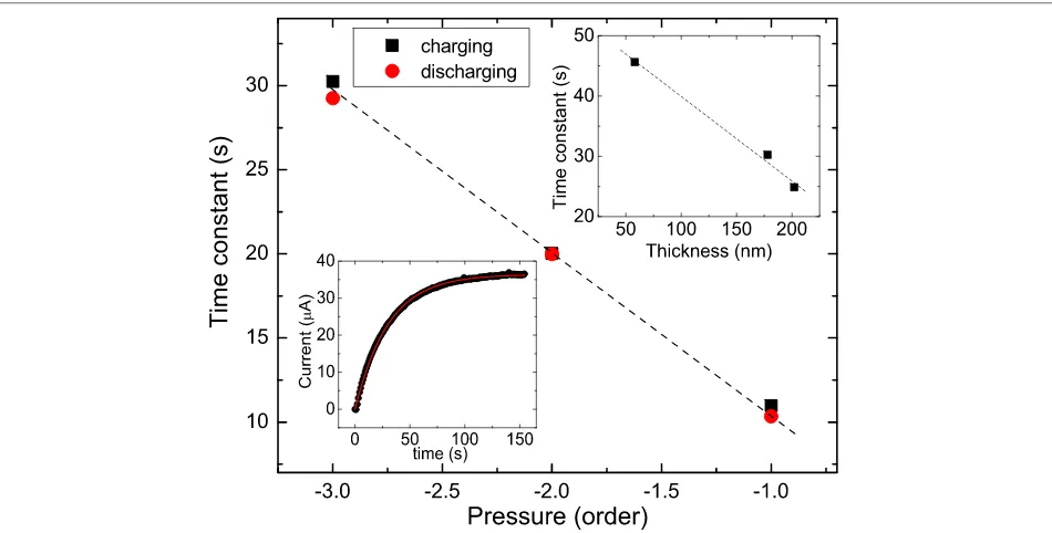
The bottom-left inset of Fig. 7 shows the photocur-rent as a function of time. The charging process could be described by the e−t/k, where k is characteristic time constant. Our experimental result reveals that the
measured photocurrent goes well with the fitting line. The top-right inset shows the extracted charge time constant as a function of thickness. It reveals that the time con-stant decreases as the thickness increases. This behavior could be understood as the uniformity current flowing process [27, 28]. On the other hand, the charge and
[image:7.595.62.538.86.308.2] [image:7.595.62.537.464.705.2]Huanget al. Nanoscale Research Letters (2018) 13:371 Page 8 of 9
discharge time constants of different atmosphere pres-sures are determined. It shows that charge time constant is roughly the same as the discharge time constants, and longer time constant is observed in lower atmosphere pressure.
Conclusion
The photocurrent was performed in the Sb2Se2Te
topo-logical insulator with different conductance at a wave-length of 532 nm. The photocurrent is linear with light power intensity, and the photocurrent is proportional to the dark current. Higher photocurrent is observed in the nanosheet with higher conductance. The responsiv-ity is proportional to the nanosheet conductivresponsiv-ity. The responsivity is independent of the light power intensity in vacuum, but responsivity drastically decreases at low power intensity in air, that is, in contrast to most reported results. The ratio of the responsivity in air to that in vacuum is negatively proportional to the the inverse of the light power intensity. These behaviors are understood as the statistical photocurrent in a system with blocked molecules. Following the theoretical model, the surface covers with adsorbed molecules by 40% in air. The time constant decreases as the thickness increases. This behav-ior could be understood as the uniformity current flowing process. The charge and discharge time constants of dif-ferent pressures are determined. A longer time constant is observed in lower atmosphere pressure. TheRand detec-tivity at V = 0.1V reaches 731 and 2.6 ×10¹⁰ at the
nanosheet with higher conductivity. These are higher than all reported values in (Sb, Bi)2(Te, Se)3topological
insu-lators and low-dimensional materials and only lower than several reported heterostructures.
Abbreviations
ARPES: Angle resolved photoemission spectroscopy; EDS: Energy-dispersive X-ray spectroscopy; SdH: Shubnikov-de Haas; XPS: X-ray photoelectron spectroscopy
Funding
The work was supported by the Taiwan National Science Council through Grants No. MOST 103-2112-M-110-009-MY3, MOST 106-2112-M-110-002, and 107-2112-M-110-011-MY2 for SMH and Grant No. MOST
105-2112-M-011-001-MY3 for RSC.
Availability of Data and Materials
The datasets generated during and/or analyzed during the current study are available from the corresponding authors on reasonable request.
Authors’ Contributions
SMH conceived the idea, analyzed the experimental results, and prepared the paper. LJL analyzed the experimental results and prepared the figures. YJY, SHY, and MMCC grew the high-quality crystal. HFH, CJH, and RSC prepared nanosheets and performed the experiment. All authors read and approved the final manuscript.
Ethics Approval and Consent to Participate
All authors agreed on the ethics approval and consent to participate.
Competing Interests
The authors declare that they have no competing interests.
Publisher’s Note
Springer Nature remains neutral with regard to jurisdictional claims in published maps and institutional affiliations.
Author details
1Department of Physics, National Sun Yat-Sen University, 80424 Kaohsiung,
Taiwan.2Department of Materials and Optoelectronic Science, National Sun
Yat-Sen University, 80424 Kaohsiung, Taiwan.3Center of Crystal Research,
National Sun Yat-sen University, Kaohsiung 80424, Taiwan.4Graduate Institute
of Applied Science and Technology, National Taiwan University of Science and Technology, 10607 Taipei, Taiwan.
Received: 2 August 2018 Accepted: 15 October 2018
References
1. Roy K, Padmanabhan M, Goswami S, Sai TP, Ramalingam G, et al. (2013) Graphene-MoS2hybrid structures for multifunctional hotoresponsive
memory devices. Nat Nanotech 8:826
2. Zhang WJ, Chuu CP, Huang JK, Chen CH, Tsai ML, et al. (2014)
Ultrahigh-Gain Photodetectors Based on Atomically Thin Graphene-MoS2
Heterostructures. Sci Rep 4:3826
3. Konstantatos G, Badioli M, Gaudreau L, Osmond J, Bernechea M, et al. (2012) Hybrid graphene-quantum dot phototransistors with ultrahigh gain. Nat Nanotech 7:363
4. Chen C, Qiao H, Lin S, Luk CM, Liu Y, et al. (2015) Highly responsive MoS2
photodetectors enhanced by graphene quantum dots. Sci Rep 5:11830 5. Soci C, Zhang A, Xiang B, Dayeh SA, Aplin DPR, et al. (2007) Self-Powered,
Ultrafast, Visible-Blind UV Detection and Optical Logical Operation based on ZnO/GaN Nanoscale p-n Junctions. Nano Lett 7:1003
6. Chen RS, Wang WC, Chan CH, Lu ML, Chen YF, et al. (2013)
Photoconduction efficiencies of metal oxide semiconductor nanowires: The material’s inherent properties. Appl Phys Lett 103:223107 7. Zhang Y, Liu T, Meng B, Li X, Liang G, et al. (2013) Broadband high
photoresponse from pure monolayer graphene photodetector. Nat Communi 4:1811
8. Mueller T, Xia F, Avouris P (2010) Graphene photodetectors for high-speed optical communications. Nat Photonics 4:297
9. Hu PA, Wen Z, Wang L, Tan P, Xiao K (2012) Synthesis of Few-Layer GaSe Nanosheets for High Performance Photodetectors. ACS Nano 6:5988 10. Hu PA, Wang L, Yoon M, Zhang J, Feng W, et al. (2013) Highly Responsive
Ultrathin GaS Nanosheet Photodetectors on Rigid and Flexible Substrates. Nano Lett 13:1649
11. Yin Z, Li H, Li H, Jiang L, Shi Y, et al. (2012) Single-Layer MoS2
Phototransistors. ACS Nano 6:74
12. Furchi MM, Polyushkin DK, Pospischil A, Mueller T (2014) Mechanisms of Photoconductivity in Atomically Thin MoS2. ACS Nano 14:6165
13. Tsai DS, Liu KK, Lien DH, Tsai ML, Kang CF, et al. (2013) Few-Layer MoS2
with High Broadband Photogain and Fast Optical Switching for Use in Harsh Environments. ACS Nano 7:3905
14. Zhang W, Huang JK, Chen CH, Chang YH, Cheng YJ, et al. (2013) High-Gain Phototransistors Based on a CVD MoS2Monolayer. Adv Mater 25:3456
15. Choi W, Cho MY, Konar A, Lee JH, Cha GB, et al. (2012) High-detectivity multilayer MoS2phototransistors with spectral response from ultraviolet
to infrared. Adv Mater 24:5832
16. Buscema M, Island JO, Groenendijk DJ, Blanter SI, Steele GA, et al. (2015) Photocurrent generation with two-dimensional van der Waals semiconductors. Chem Soc Rev 44:3691
17. Yazyev OV, Chen YP (2014) Polycrystalline graphene and other two-dimensional materials. Nat Nanotechnol 9:755
18. Gong C, Hu K, Wang X, Wangyang P, Yan C, et al. (2018) 2D Nanomaterial Arrays for Electronics and Optoelectronics. Adv Funct Mater 28:1706559 19. Gong C, Zhang Y, Chen W, Chu J, Lei T, et al. (2017) Electronic and
Optoelectronic Applications Based on 2D Novel Anisotropic Transition Metal Dichalcogenides. Adv Sci 4:1700231
20. Yan C, Gan L, Zhou X, Guo J, Huang W, et al. (2017) Space-Confined Chemical Vapor Deposition Synthesis of Ultrathin HfS2Flakes for
Optoelectronic Application. Adv Funct Mater 27:1702918 21. Chu J, Wang F, Yin L, Lei L, Yan C, et al. (2017) High-Performance
Ultraviolet Photodetector Based on a Few-Layered 2D NiPS3Nanosheet.
22. Wangyang P, Gong C, Rao G, Hu K, Wang X, et al. (2018) Recent Advances in Halide Perovskite Photodetectors Based on Different Dimensional Materials. Adv Opt Mater 6:1701302
23. Braun L, Mussler G, Hruban A, Konczykowski M, Schumann T, et al. (2016) Ultrafast photocurrents at the surface of the three-dimensional topological insulator Bi2Se3. Nat Commun 7:13259
24. McIver JW, Hsieh D, Drapcho SG, Torchinsky DH, Gardner DR, et al. (2012) Theoretical and experimental study of second harmonic generation from the surface of the topological insulator Bi2Se3. Phys Rev B 86:035327
25. Zhang H, et al. (2016) High-Responsivity, High-Detectivity, Ultrafast Topological Insulator Bi2Se3/Silicon Heterostructure Broadband
Photodetectors. ACS Nano 10:5113
26. Liu C, et al. (2016) Topological insulator Bi2Se3nanowire/Si
heterostructure photodetectors with ultrahigh responsivity and broadband response. J Mater Chem C 4:5648
27. Hunag SM, Huang SJ, Yan YJ, Yu SH, Chou M, et al. (2017) Extremely high-performance visible light photodetector in the Sb2SeTe2nanoflake.
Sci Rep 7:45413
28. Hunag SM, Huang SJ, Yan YJ, Yu SH, Chou M, et al. (2017) Highly responsive photoconductance in a Sb2SeTe2topological insulator
nanosheet at room temperature. RSC Adv 7:39057
29. Huang SM, Yan YJ, Yu SH, Chou M (2017) Thickness-dependent conductance in Sb2SeTe2topological insulator nanosheets. Sci Rep
7:1896