Fumin Li
, Mengqi Xu
, Xingping Ma
, Liang Shen
, Liangxin Zhu
, Yujuan Weng
, Gentian Yue
,
Furui Tan
1,2and Chong Chen
1,2*Abstract
We report a new method as UV treatment of low-temperature processed to obtain tin oxide (SnO2) electron transport layers (ETLs). The results show that the high quality of ETLs can be produced by controlling the thickness of the film while it is treated by UV. The thickness is dependent on the concentration of SnO2. Moreover, the conductivity and transmittance of the layer are dependent on the quality of the film. A planar perovskite solar cell is prepared based on this UV-treated film. The temperatures involved in the preparation process are less than 90 °C. An optimal power conversion efficiency of 14.36% is obtained at the concentration of SnO2of 20%. This method of UV treatment SnO2 film at low temperature is suitable for the low-cost commercialized application.
Keywords:UV treatment, Low-temperature, Tin oxide, Perovskite solar cells
Background
Perovskite solar cells (PSCs) have attracted enormous research interest in recent years with power conversion efficiencies (PCE) enhancing from 3.8 to 22.1% [1–8]. In a typical perovskite solar cell either with or without meso-porous scaffold, an absorber layer is sandwiched between electrode-modified layers including the electron and hole transport layers (ETLs and HTLs, respectively), namely the mesoporous scaffold and planar hetero-junction archi-tectures [9–11]. The high quality of the perovskite layer, which is smooth, compactive, and uniform, has a crucial impact on the device performance [12–14]. However, the quality of the bottom modified layer can directly affect the preparation of perovskite film. Typically, spin-coating method [15–17], hydrothermal synthesis method [18,19], vacuum evaporation method [20], atomic layer deposition method [21], and electro-chemical deposition [22, 23] were adopted to improve the quality of the modified layers. And then, a compact modified layer was obtained by annealing and sintering at high temperature. The temperature is up to 450 and 180 °C when using TiO2
[24–27] and SnO2 [28–31] as the modified layer, respectively. The TiO2was obtained by heat treatment of tetrabutyl titanate precursor, and the SnO2 was obtained by treatment of SnCl2precursor [32]. However, the high temperature is not suitable for modern industrial manufacture.
To solve this problem, we present our preparation of compact layer by spin-coating SnO2precursor and then treating by ultraviolet ozone (UVO). Here, tin oxide water solution is used as raw materials of SnO2. Moreover, the temperatures on each layer of the preparation of PSC are all at low temperature (less than 90 °C). It is easier to re-duce technological difficulty of preparation process and to reduce production cost, which will be suitable for the in-dustrial production. Our cells are based on CH3NH3PbI3 (MAPbI3), as a narrow band gap and high absorption ma-terial of visible light, which is processed by means of a one-step anti-solvent (OSAS) method [33–37]. The archi-tecture of the planar hetero-junction PSC is Glass/ITO/ SnO2/MAPbI3/Spiro-OMeTAD/Au. The MAPbI3is sand-wiched between SnO2 ETLs and Spiro-OMeTAD HTLs, respectively. After analyzing the surface morphology, sur-face element distribution, and light transmittance of the films, our results demonstrate that the SnO2-modified layer with compactness, purity, and high transmittance
* Correspondence:lifm@henu.edu.cn;chongchen@henu.edu.cn
1Henan Key Laboratory of Photovoltaic Materials, Henan University, 1 Jinming
Road, Kaifeng 475004, People’s Republic of China
Full list of author information is available at the end of the article
can be prepared by spin-coating and UVO treatment. Moreover, the high-performance planar PSCs were pre-pared at low temperature. The PCE of the PSC is 14.5% by optimizing the conditions of device preparation.
Methods
Materials and Precursor Preparation
Methylammonium iodide (MAI; Z99.5%) and lead iodide (PbI2; Z99.9%) were purchased from the Xi’an Polymer Light Technology Corp. Tin oxide (SnO2; 15% mass in H2O colloidal dispersion with a few organic solvents) was purchased from Alfa Aesar. 1,2-Dichlorobenzene (DCB; 99.5%) was purchased from J&K Scientific Ltd.
N,N-Dimethylformamide (DMF; 99%), dimethylsulfoxide (DMSO; 99%), 2,2′, 7,7′-tetrakis(N,N -p-dimethoxyphe-nylamino)-9,9′-spirobifluorene (Spiro-OMeTAD), 4-tert-butylpyridine (TBP), and bis(trifluoromethylsulfo-nyl)-imide lithium salt (Li-TFSI) were purchased from Sigma Aldrich. Gold (Au; 99.995%) was purchased from China New Metal Materials Technology Co., Ltd. All the reagents were used without further purification.
Fabrication of Devices
The PSC device has a structure of ITO/SnO2/MAPbI3/ Spiro-OMeTAD/Au. The ITO glass plates (a sheet resist-ance of < 15Ω/□) were pre-cleaned in an ultrasonic bath with acetone, ethanol, and de-ionized (DI) water for 15 min each, followed by drying with a nitrogen flow. Subsequently, the substrates were treated using ultravio-let ozone cleaner for 15 min at about 60 °C. The SnO2 thin films were prepared by spin-coating the SnO2(xas 10, 15, 20, and 30%) precursor solution on the clean ITO glass substrates at 5000 rpm for 30 s and dried at
50 °C for 5 min, then treated by ultraviolet ozone cleaner for 60 min at about 60 °C. The solution concentrations of precursor were changed to 10, 15, 20, and 30% by diluting or condensing the original solution. A 1-M per-ovskite precursor of MAPbI3was prepared by dissolving MAI and PbI2in a 1:1 M ratio in 9:1 (v:v) mixed solvent of DMF and DMSO. Then, the precursors were stirred and heated at 50 °C overnight. For the active layer, the perovskite precursor was spin-coated at 4000 rpm. for 30 s on top of the SnO2 surface. Diethyl ether, as an anti-solvent agent, was drop-cast on the substrate at 5 s before the end of the spin. The samples were subsequently annealed at 90 °C for 10 min on hotplate in a glove-box and then cooled down for a few minutes. The typical thickness of MAPbI3was about 300 nm. For
HTM layer, 30 μL solution composing of 70 mM
spiro-OMeTAD, 28.8 mM Li-TFSI, and 55 mM TBP in DCB was spin-coated on the perovskite layer at 5000 rpm. for 20 s. Finally, 100 nm of Au was thermally evaporated under high vacuum (5 × 10⁻⁴Pa). The depos-ition rate which was monitored with a quartz oscillating thickness monitor (ULVAC, CRTM-9000) was approxi-mately 5 Å/s. The active area of the device is 4 mm2.
[image:2.595.58.540.88.218.2]Fig. 1Surface SEM image of SnO2(a) and the corresponding EDX spectra of ITO/SnO2film
Table 1Specific content of each element
Element Wt% At%
CK 00.42 00.92
OK 49.29 87.82
SnL 50.29 11.26
[image:2.595.306.537.550.713.2] [image:2.595.55.291.661.733.2]Characterization and Measurements
Current density–voltage (J-V) characteristics were measured using a computer-programmed Keithley 2400 source/meter under AM1.5G solar illumination using a Newport 94043A solar simulator. The intensity of the solar simulator was 100 mW/cm2. Light intensity was corrected by a standard silicon solar cell. The transmission spectrum was measured using ultraviolet/visible (UV–vis) spectrom-eter (Carry 5000). The surface morphology and structure of the as-prepared films were characterized using SEM (JSM-7001F, Japan Electron Optics Laboratory Co., Japan). The crystalline phase of as-prepared SnO2film was con-firmed by power X-ray diffractometry (XRD) (DX-2700, Dandong Fangyuan Instrument Co.Ltd., Dandong, China).
Results and Discussion
The UV/ozone can produce ultraviolet light that peaks nearly at 185 and 254 nm with photon energy of 647 and 472 kJ/mol, respectively, which are higher than the bond energy of C-C, C-O, and C-H of 346, 358, and 411 kJ/mol, respectively [38–40]. As a result, the UV light will easily
break these chemical bonds while treating. In order to confirm it, SnO2 film with a concentration of 20% is selected for elemental distribution spectrometer (EDS) after UV treatment, and the distribution of the main components is investigated. Figure 1ashows the SEM of the selected film. The evenness and uniformity of the film are good at large scale at the bar of 0.5 um. Figure 1b
shows the element distribution diagram, while the peak without mark is the peak position of the test electrode gold. As you can see, the Sn, O, and trace C element are included. Table1is the specific content of each element in the selected film. After UV treatment, the content of Sn and O in the film is greater than 99%, and the content of C is less than 1%. It can be recognized that most of the organic solvents are removed, and only Sn and O are left after UV treatment. So this way of processing can get the high purity SnO2 ETLs, which provides a possibility for the preparation of high-performance PSCs. Figure2shows the XRD pattern of SnO2 on slide glass after UV treat-ment. The XRD profile shows diffraction peaks at 2θ values of 26.5°, 34.0°, 38.1°, 51.6°, and 65.9°, which are identified as the reflections from (110), (101), (200), (211), and (301) planes of the rutile type tetragonal structure of SnO2(JCPDS41-1445), respectively. The crystallite size of SnO2was calculated using the Debye–Scherrer eq. (D= 0.89λ/βcosθ) [41], whereDis mean crystallite size,λis the X-ray wavelength,θis the Bragg diffraction angle, andβis the peak width at half maximum. It provides an estimated crystallite size of 5.5 nm for the as-prepared sample.
Figure3ais the structure diagram of the PSC. Figure3b
is the surface SEM image of the active layer, and the
Fig. 3Structure diagram of the perovskite solar cell (a) and the SEM image of active layer (b)
[image:3.595.57.539.88.220.2]Fig. 4J-Vcharacteristics of the device. The characteristics depend on the different concentrations of SnO2which are varied from 10 to 30% under AM1.5G illumination of 100 mW/cm2. The inset shows the corresponding PCE-Vcurve
Table 2Summary of PSC performance under illumination of 100 mW/cm2
Concentration Voc(V) Jsc(mA/cm2) PCE (%) FF Rs (Ω) Rsh (Ω)
10% 1.08 17.92 13.32 0.688 265.4 42,011
15% 1.07 19.44 13.55 0.651 202.9 30,857
20% 1.11 20.11 14.36 0.643 182.8 15,868
[image:3.595.57.290.522.683.2] [image:3.595.304.540.661.731.2]illustration is a cross-sectional view of the ITO/SnO2 (20%) /MAPbI3. It can be observed that the continuity of perovskite film is good. The particle size of the single perovskite crystal is larger than 1 μm; the transverse crystallization of the active layer is very good. The thick-ness of SnO2(20%) is about 65 nm, and the thickness of perovskite is about 384 nm, which is expected to obtain high-performance perovskite solar cell.
As shown in Fig. 4, the J-V characteristic curves of device ITO/SnO2(x)/MAPbI3/Spiro-OMeTAD/Au (x= 10, 15, 20, and 30%) under AM1.5G solar illumination of 100 mW/cm2 in ambient air. The detailed results are given in Table2. It shows thatJscof device increase first and then decrease with the increase of SnO2 concentra-tion. Jsc of the device with 10% is the smallest and that with 20% is the largest. The probable reason is, when the concentration of SnO2 is changed, that the thickness of film increases which leads to increase resistance. More-over, the light transmittance of film will be different due to the different thickness. Voc of device increases with concentration of SnO2 increasing. The thick SnO2 film reduces the probability that the holes transport to the FTO electrode, which is easy to achieve for electrons. It is advantageous to reduce the recombination of carriers at
the interface. When the concentration of SnO2was 20%, the PSCs obtain an optimal performance with Jsc of 20.11 mA/cm2,Vocof 1.11 V, FF of 0.643, PCE of 14.36%, Rs of 232.8Ω, and Rsh of 15,868Ω.
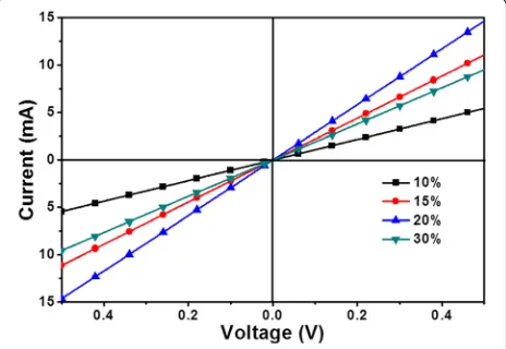
Figure5shows the cross-sectional SEM images of SnO2 films. The image scale bar of the films is 100 nm, and its magnification is × 100,000. The thicknesses of the films which were prepared at different concentrations of SnO2 were 34 nm at 10%, 48 nm at 15%, 66 nm at 20%, and 97 nm at 30%, respectively. The thickness increased grad-ually by the increasing concentration of SnO2. In order to understand the influence on the vertical resistance of the thickness of SnO2films, a resistance device was prepared with a structure as ITO/SnO2(x)/Au. Figure6 shows the I-V curves. The resistance between ITO and Au were 98.6Ωat 10%, 41.6 at 15%, 33.7 at 20%, and 50.8 at 30%. When the concentrations changed from 10 to 20%, the vertical resistance reduced, which increased when the concentration was up to 30%. It differs from the conven-tional knowledge that the resistance increases with the increase of thickness. To further analyze the reasons, the surface SEM of the films was investigated.
Figure 7a–d shows the top view SEM images of SnO2 films at × 50,000 magnification with a scale bar of 100 nm. And Fig. 7e–h shows the corresponding surface SEM images at × 200,000 magnification with a scale bar of 100 nm. It can be seen that the uniformity and smooth-ness of the films are very good at various concentrations, and the typical crystallite size of SnO2is about 6.814 nm, which is quite approximate to that calculated of Debye– Scherrer eq. (5.5 nm), so that the high-quality active layer should be obtained when preparing the perovskite absorb-ance layer. There are just a few minor differences between them. This slight difference should be the reason that affects resistance. When the SnO2concentration is 10%, the continuity of the films is poor, and some island groups appeared as shown in Fig. 7a, e. These defects on the surface introduce partial resistance value. The films are obviously uniform and even when the concentration increases to 20% as shown in Fig.7b, c, f, g,which leads to
Fig. 5Cross-sectional SEM images ofathe ITO/SnO2(10%),bITO/SnO2(15%),cITO/SnO2(20%), anddITO/SnO2(30%)
[image:4.595.58.540.88.219.2] [image:4.595.58.290.555.715.2]an increase in electrical conductivity. While the concen-tration is up to 30%, the reunion situation is appeared which leads to an increase in the resistance. Moreover, the light transmittance of film was depended by the thickness of the modified layer, which affected the utilization of light by active materials.
In order to understand the cause, we had tested the UV–vis transmission spectrum of the SnO2(x) films, as shown in Fig. 8. It can be seen that the transmittance of the films exceeds 75% between 400 and 800 nm. The peaks are right on 616, 662, 718 nm, and more than 800 nm when the concentrations are 10, 15, 20, and 30%, respectively. With the increase of the thickness of SnO2, the transmission peak is red shifted. The absorption range of the MAPbI3is between 300 and 760 nm. The transmit-ted lights are matched with that absorption range of perovskite while the concentrations are less than 20%. Therefore, the higher PCE could be obtained due to the more light utilization. When the concentration is 30%, the light absorption of active layer is attenuated that leads to a decrease in PCE. The utilization of light influences the
performance of the PSCs. As a result, the PCE will be increased first and then decreased with the increase of concentration, which coincides with the previous results.
Conclusions
In summary, we demonstrated a novel method as UVO treatment at low temperature which a high-quality SnO2 ETL could be prepared. High-performance PSCs were obtained by OSAS method. When the concentration of SnO2was 20%, the PSCs obtained an optimal performance with PCE of 14.36%. The analysis results are shown that the conductivity and transmittance of the modified layer were depended on the thickness and uniformity of the film, and high-performance PSC could be obtained at suitable thickness of the modified film.
Abbreviations
ETLs:Electron transport layers; FF: Fill factor; HTLs: Hole transport layers;
Jsc: Short-circuit photocurrent; OSAS: One-step anti-solvent; PCE: Power conversion efficiencies; PSCs: Perovskite solar cells; UVO: Ultraviolet ozone;
Voc: Open-circuit voltage
Acknowledgements
The authors gratefully acknowledge the financial support provided by the Science Foundation of Henan University and the Natural Science Foundation of Henan Province.
Funding
This work was supported by the Science Foundation of Henan University (Grant No. zzjj20170007) and the Natural Science Foundation of Henan Province (Grant No. 162300410021).
Availability of Data and Materials Please contact the author for data requests.
Authors’Contributions
FL carried out the experiments, participated in the sequence alignment, and drafted the manuscript. MX and CC participated in the device preparation. XM, LS, LZ, YW, GY, FT, and CC were involved in the SEM, EDS, and UV–vis analysis of the devices. All authors read and approved the final manuscript.
Competing Interests
The authors declare that they have no competing interests.
Fig. 7Top view SEM images ofa–dthe prepared ITO/SnO2(x) films at × 50,000 magnification, ande–hfilms at × 200,000 magnification
[image:5.595.59.539.88.255.2] [image:5.595.58.292.557.714.2]References
1. Kojima A, Teshima K, Shirai Y, Miyasaka T (2009) Organo-metal halide perovskites as visible-light sensitizers for photovoltaic cells. J Am Chem Soc 131:6050–6051
2. Im JH, Lee CR, Lee JW, Park SW, Park NG (2011) 6.5% efficient perovskite quantum-dot-sensitized solar cell. Nanoscale 3:4088–4093
3. Stranks SD, Eperon GE, Grancini G, Menelaou C, Alcocer MJ, Leijtens T, Herz LM, Petrozza A, Snaith HJ (2013) Electron-hole diffusion lengths exceeding 1 micrometer in an organometal trihalide perovskite absorber. Science 342:341–344
4. Zhou HP, Chen Q, Li G, Luo S, Song TB, Duan HS, Hong Z, You J, Liu Y, Yang Y (2014) Interface engineering of highly efficient perovskite solar cells. Science 345:542–546
5. Jeon NJ, Noh JH, Yang WS, Kim YC, Ryu S, Seo J, Seok SI (2015) Compositional engineering of perovskite materials for high-performance solar cells. Nature 517:476–480
6. Yang WS, Noh JH, Jeon NJ, Kim YC, Ryu SC, Seo JW, Seok SI (2015) High-performance photovoltaic perovskite layers fabricated through intra-molecular exchange. Science 348:1234–1237
7. Bi D, Yi CY, Luo JS, Décoppet JD, Zhang F, Zakeeruddin SM, Li X, Hagfeldt A, Grätzel M (2016) Polymer-templated nucleation and crystal growth of perovskite films for solar cells with efficiency greater than 21%. Nat Energy 1:16142
8. Yang WS, Park BW, Jung WH, Jeon NJ, Kim YC, Lee DU, Shin SS, Seo JW, Kim EK, Noh JH, Seok SI (2017) Iodide management in formamidinium-lead-halide- based perovskite layers for efficient solar cells. Science 356:1376–1379
9. Guo MX, Li FM, Ling LY, Chen C (2017) Electrochemical and atomic force microscopy investigations of the effect of CdS on the local electrical properties of CH3NH3PbI3:CdS perovskite solar cells. J Mater Chem C 5:12112 10. Bisquert J, Qi YB, Ma TL, Yan YF (2017) Advances and obstacles on
perovskite solar cell research from material properties to photovoltaic function. ACS Energy Lett 2:520–523
11. Mali SS, Kim HJ, Kim HH, Shim SE, Hong CK (2018) Nanoporous p-type NiOxelectrode for p-i-n inverted perovskite solar cell toward air stability. Mater Today 2:xxx
12. Yue SZ, Lu SD, Ren KK, Liu K, Azam M, Cao DW, Wang ZJ, Lei Y, Qu SC, Wang ZG (2017) Insights into the influence of work functions of cathodes on efficiencies of perovskite solar cells. Small 13:1–7
13. Yue SZ, Liu K, Xu R, Li MC, Azam M, Ren KK, Liu J, Sun Y, Wang ZJ, Cao DW, Yan XH, Qu SC, Lei Y, Wang ZG (2017) Efficacious engineering on charge extraction for realizing highly efficient perovskite solar cells. Energy Environ Sci 10:2570–−2578
14. Azam M, Yue SZ, Liu K, Sun Y, Liu J, Ren KK, Wang ZJ, Qu SC, Wang ZG (2017) Insights on the correlation of precursor solution, morphology of the active layer and performance of the pervoskite solar cells. J Alloy Compd 731:375–380
15. Gao P, Grätzel M, Nazeeruddin MK (2014) Organohalide lead perovskites for photo-voltaic applications. Energy Environ Sci 7:2448
16. Jiang Q, Chu ZM, Wang PY, Yang XL, Liu H, Wang Y, Yin ZG, Wu JL, Zhang XW, You JB (2017) Planar-structure perovskite solar cells with efficiency beyond 21%. Adv Mater 29:1703852
17. Singh T, Miyasaka T (2017) Stabilizing the efficiency beyond 20% with a mixed cation perovskite solar cell fabricated in ambient air under controlled humidity. Adv Energy Mater 8:1700677
MK, Grätzel M (2013) Low-temperature crystalline titanium dioxide by atomic layer deposition for dye-sensitized solar cells. ACS Appl Mater Interfaces 5:3487–3493
22. Kavan L, O’Regan B, Kay A, Grätzel M (1993) Preparation of TiO2 (anatase) films on electrodes by anodic oxidative hydrolysis of TiCl3. J Electroanal Chem 346:291–307
23. Ke WJ, Fang GJ, Wang J, Qin PL, Tao H, Lei HW, Liu Q, Dai X, Zhao XZ (2014) Perovskite solar cell with an efficient TiO2compact film. ACS Appl Mater Interfaces 6:15959–15965
24. Xu YH, Shi JW, Lv ST, Zhu LF, Dong J, Wu HJ, Xiao Y, Luo YH, Wang SR, Li DM, Li XG, Meng QB (2014) Simple way to engineer metal −semiconductor interface for enhanced performance of perovskite organic lead iodide solar cells. ACS Appl Mater Interfaces 6:5651–5656 25. Fabregat-Santiago F, Kulbak M, Zohar A, Valles-Pelarda M, Hodes G,
Cahen D, Mora-Sero I (2017) Deleterious effect of negative capacitance on the performance of halide perovskite solar cells. ACS Energy Lett 2:2007–2013
26. Saliba M, Matsui T, Seo JY, Domanski K, Correa-Baena JP, Nazeeruddin MK, Zakeeruddin SM, Tress W, Abate A, Hagfeldtd A, Grätzel M (2016) Cesium-containing triple cation perovskite solar cells: improved stability, reproducibility and high efficiency. Energy Environ Sci 9:1989–1997 27. Wang SH, Jiang Y, Juarez-Perez EJ, Ono LK, Qi YB (2017) Accelerated
degradation of methylammonium lead iodide perovskites induced by exposure to iodine vapour. Nat Energy 2:16195
28. Ke WJ, Fang GJ, Liu Q, Xiong LB, Qin PL, Tao H, Wang J, Lei HW, Li BR, Yang G, Yan YF (2015) Low-temperature solution-processed tin oxide as an alternative electron transporting layer for efficient perovskite solar cells. J Am Chem Soc 137:6730–6733
29. Wang ZP, Lin QQ, Chmiel FP, Sakai N, Herz LM, Snaith HJ (2017) Efficient ambient-air-stable solar cells with 2D–3D heterostructured butylammonium-caesium-formamidinium lead halide perovskites. Nat Energy 2:17135
30. Brenes R, Guo DY, Osherov A, Noel NK, Eames C, Hutter EM, Pathak SK, Niroui F, Friend RH, Islam MS, Snaith HJ, BulovićV, Savenije TJ, Stranks SD (2017) Metal halide perovskite polycrystalline films exhibiting properties of single crystals. Joule 1:155–167
31. Habisreutinger SN, Wenger B, Snaith HJ, Nicholas RJ (2017) Dopant-free planar n−i−p perovskite solar cells with steady-state efficiencies exceeding 18%. ACS Energy Lett 2:622–628
32. Tong X, Lin F, Wu J, Wang ZM (2016) High performance perovskite solar cells. Adv Sci 3:1500201
33. Sun JC, Wu J, Tong X, Lin F, Wang YN, Wang ZM (2018) Organic/ inorganic metal halide perovskite optoelectronic devices beyond solar cells. Adv Sci 5:1700780
34. Shi D, Adinolfi V, Comin R, Yuan MJ, Alarousu E, Buin A, Chen Y, Hoogland S, Rothenberger A, Katsiev K, Losovyj Y, Zhang X, Dowben PA, Mohammed OF, Sargent EH, Bakr OM (2015) Low trap-state density and long carrier diffusion in organolead trihalide perovskite single crystals. Science 347:519–522
35. Zhang W, Eperon GE, Snaith HJ (2016) Metal halide perovskites for energy applications. Nate Energy 1:16048
36. Liang J, Liu J, Jin Z (2017) All-inorganic halide perovskites for optoelectronics: progress and prospects. Solar RRL 1:1700086 37. Seok SI, Grätzel M, Park NG (2018) Methodologies toward highly
efficient perovskite solar cells. Small 14:1704177