N A N O E X P R E S S
Open Access
Si solid-state quantum dot-based materials for
tandem solar cells
Gavin Conibeer
*, Ivan Perez-Wurfl, Xiaojing Hao, Dawei Di and Dong Lin
Abstract
The concept of third-generation photovoltaics is to significantly increase device efficiencies whilst still using thin-film processes and abundant non-toxic materials. A strong potential approach is to fabricate tandem cells using thin-film deposition that can optimise collection of energy in a series of cells with decreasing band gap stacked on top of each other. Quantum dot materials, in which Si quantum dots (QDs) are embedded in a dielectric matrix, offer the potential to tune the effective band gap, through quantum confinement, and allow fabrication of optimised tandem solar cell devices in one growth run in a thin-film process. Such cells can be fabricated by sputtering of thin layers of silicon rich oxide sandwiched between a stoichiometric oxide that on annealing crystallise to form Si QDs of uniform and controllable size. For approximately 2-nm diameter QDs, these result in an effective band gap of 1.8 eV. Introduction of phosphorous or boron during the growth of the multilayers results in doping and a rectifying junction, which demonstrates photovoltaic behaviour with an open circuit voltage (VOC) of
almost 500 mV. However, the doping behaviour of P and B in these QD materials is not well understood. A modified modulation doping model for the doping mechanisms in these materials is discussed which relies on doping of a sub-oxide region around the Si QDs.
Keywords:band gap engineering, quantum dots, photovoltaics, tandem cells, modulation doping, nucleation, third generation
Introduction
An increase in efficiency can be achieved through the use of multiple energy levels in a third-generation photovoltaic device. One configuration which increases the voltage output from the device is the tandem or multi-junction cell, in which cells with increasing band gap are stacked on top of each other such that each cell absorbs a different part of the solar spectrum with a narrower range and hence more optimally for each absorbed photon. The sum of the output from these cells can boost the overall efficiency. In practice, it is easiest to configure the cells such as to have the same current through each cell in an in-series or current-matched two-terminal device.
The Si quantum dot (QD) solar cell is suggested as a way to engineer the band gap (Eg) of the top cell or cells in a tandem stack using thin-film deposition meth-ods [1-3]. The very small scale of QDs of a few
nanometers, and hence less than the Bohr radius of Si, results in increased confined energy levels through quantum confinement. For QDs the effect is stronger than quantum wells because confinement is in all three dimensions. For QDs which are close to each other such that there is a significant tunnelling probability, a true miniband will form and result in an increase in the effective band gap of the tailored superlattice material. The conceptual design of a complete device is shown in Figure 1.
Incorporation of P or B during growth results in n- or p-type materials, respectively, and allows growth of rec-tifying junctions, which have photovoltaic properties. Si QD devices have been demonstrated by some of the current authors with VOCup to 490 mV [4-7]. However, further optimisation of these materials and devices such as to increaseVOC and improve the presently very low current densities (tens of microamperes per square cen-timetre) requires a better understanding of the exact mechanisms of doping.
* Correspondence: [email protected]
ARC Photovoltaics Centre of Excellence, University of New South Wales, Sydney, NSW 2052, Australia
Fabrication of Si QD nanostructures
Structures are grown using magnetron sputtering on quartz substrates. Alternating layers of a Si-rich dielec-tric and a stoichiomedielec-tric layer of dielecdielec-tric are depos-ited. Layer thicknesses are kept constant within one structure, although the stoichiometric dielectric may well have a different thickness to the Si-rich layer. Layer thicknesses are varied from sample to sample between 2 and 7 nm. The number of bi-layers is also varied but is typically between 20 and 40. The dielectric used is usually SiO2, although Si3N4and SiC are also used. This layer growth technique for SiO2was borrowed from [8] and adapted for photovoltaics by [1].
Post-deposition, the structures are annealed typically at 1,050 to 1,150°C for 1 to 2 h. During this process, the high temperature nucleates the growth of small nano-crystals from the excess Si in the Si-rich layers. These nanocrystals grow depending on the growth time until all the excess Si has diffused to growing nanocrystals. The size of these nanocrystals is limited by the border with the stoichiometric dielectric region in which there is no excess Si to diffuse. This results in a fairly uniform nanocrystal size which is desirable for the formation of quantum dots with fairly uniform confined energy level as it increases the probability of formation of a true miniband. This process is shown schematically in Figure 2.
For Si QDs in SiO2, the precipitation occurs according to the following:
SiOx→ x
2SiO2+
1− x 2
Si (1)
Precipitation of excess Si from Si-rich dielectrics in SiNx and SiCxfollows a similar crystallisation reaction
as Si precipitates from the amorphous matrix.
The decreasing barrier height on going from SiO2 to Si3N4 to SiC is used to increase the tunnelling
probability between adjacent quantum dots or between quantum dot layers. Si3N4 and SiC give lower barriers than SiO2allowing larger dot spacing for a given tunnel-ling current. The wave function of an electron confined to a spherical dot penetrates into the surrounding mate-rial, decreasing exponentially into the barrier. The slope of this exponential decay and hence the barrier to tun-nelling between quantum dots is reduced for a lower barrier height material. This is because - from transmis-sion/reflection probability - the tunnelling probability Te through a square potential well depends exponentially on three parameters, the barrier width, d(equal to the spacing between quantum dots); the square root of the barrier height seen by the electron (ΔE1/2, the energy difference between the CB edge of the matrix and the confined energy level of the quantum dots, equivalent to (Ec-En)1/2); and the square root of the effective mass (m*)1/2 of the electron in the barrier. This gives the approximate relation (e.g. [9], p. 244):
Te≈16 exp
−d
8m∗ ¯ h2 E
(2)
Fluctuations in spacing and size of the dots around their mean values can be investigated using similar cal-culations. Using this approach, it is also found that the calculated Bloch mobilities do not depend strongly on variability in the dot position around a mean position,
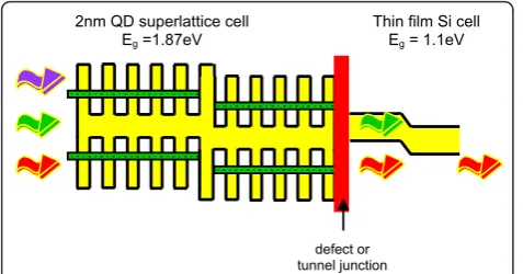
Δd, but do depend strongly on variation in the dot size within the QD material [10]. This is an important result for engineering a real thin-film structure, because although it is necessary to have a reasonably uniform QD size and to minimise the mean spacing between QDs, d, to give high mobilities for a given matrix, the variation around this mean value, Δd, is less critical. Hence, transport between dots can be significantly Thin film Si cell
Eg = 1.1eV
2nm QD superlattice cell Eg =1.87eV
[image:2.595.304.542.86.226.2]defect or tunnel junction
Figure 1Si nanostructure/Silicon tandem cell. The nanostructure cell consists of a multilayer structure of Si QDs in an amorphous dielectric matrix, with a junction between p-type and n-type material, all connected by a defect tunnel junction to a thin-film Si cell.
zG
Quartz or glass substrate
Si rich dielectric 2-5nm
Stoichiometric dielectric, 2-5nm
Figure 2Multilayer deposition of alternating Si-rich dielectric
and stoichiometric dielectric in layers of a few nanometers. On
[image:2.595.56.295.89.214.2]increased by using alternative matrices with a lower bar-rier height,ΔE.
Optical absorption properties of Si nanostructures The measured optical absorption for Si QD in SiO2 materials, for multilayered Si nanostructured material of various Si content, is shown in Figure 3[11]. There is a clear region of high absorption coefficient for photon energies above about 3 eV. As the Si content of the layers increases (i.e. as xdecreases) the strength of this absorption increases. This is because there is more Si to absorb photons, most of which is bound up in precipi-tated Si QDs. In addition to this onset of strong absorp-tion, it is clear from Figure 3 that there is also a significant weak absorption tail below 3 eV. This does not have a dependence on Si content.
This suggests the presence of a weakly absorbing background surrounding the crystalline Si QDs. The small dependence of absorption of this region on the Si content suggests it is a sub-stoichiometric oxide with only a very small amount of O. The identification of this sub-oxide region is important for the possible mod-ulation doping of this region by incorporated P or B atoms, as discussed below in‘Doping mechanisms for Si QD superlattice structures’ section, as a theory to explain doping behaviour.
Further evidence for the presence of such a sub-oxide region is given by a study by Daldosso et al. for very similar Si nanocrystals material in SiO2 [12]. In this work, experimental data on X-ray absorption and energy-filtered TEM clearly show the presence of amor-phous Si sub-stoichiometric oxide regions around Si nanocrsystals, with these regions extending for at least 1
nm. They further use ab initio methods to model the energy levels associated with an interface between nano-crystals and a stoichiometric SiO2 matrix which has an influence on absorption and light emission properties. This is very consistent with the sub-oxide region pro-posed around Si nanocrystals in the current work.
Doping and device fabrication for QD nanostructures
Doping in these multilayer QD structures is achieved by incorporation of either phosphorous pentoxide for n-type doping or boron for p-n-type doping into the Si-rich material by co-sputtering during growth of the appropri-ate layers. To obtain a p-n junction, several layers (typi-cally 20) doped with P2O5 are followed by several more (again typically 20) doped with B, sometimes with a few undoped layers in-between. The sample is then annealed at approximately 1,100°C to form Si QDs and to activate these dopants. Typically, hydrogenation is then per-formed in a cold-wall vacuum system at 600-625°C for 15 min.
p-n junction devices, fabricated in this way, exhibit photovoltaic properties [5]. Current-voltage (I-V) mea-surements in the dark and under 1-sun illumination indicate a good rectifying junction and generation of an open circuit voltage, VOC, up to 492 mV [4]. The high sheet resistance of the deposited layers, in conjunction with the insulating quartz substrates, causes an unavoid-able very high series resistance in the devices. The high resistance severely limits both the short circuit current and the fill factor of the cells, particularly under illumi-nation. It also makes it necessary to include effects due to in-plane current flow in the analysis of the measured electrical characteristics [6].
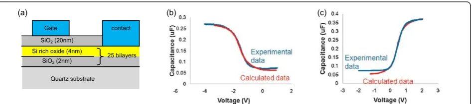
In related works, very significant decreases in resistiv-ity have been observed in B- [13] and P-doped [5] mate-rials, with related reductions in activation energy from resistance with temperature measurements. Further strong evidence for doping is shown in [14]C-Vdata for metal-oxide semiconductor (MOS) structures grown using Si-rich oxide multilayer structures as shown sche-matically in Figure 4a. TheC-Vdata for Boron-doped silicon-rich oxide (SRO) in Figure 4b show that for a negatively biased gate, the sample exhibits accumulation, indicating p-type behaviour as a significant capacitance accumulates across the 20 nm oxide layer. Whereas for phosphorous-doped SRO Figure 4c shows inversion for the same negative bias on the gate, indicating n-type behaviour with minimal accumulation across the oxide. The modelled fit to these data is for a 4 × 1017-cm-3 hole and 1 × 1017-cm-3electron concentration for B and P doping, respectively. These data clearly show that p-type and n-p-type doping occur on incorporation of B and P respectively, although the exact nature of doping in
5.5 5.0 4.5 4.0 3.5 3.0 2.5 2.0 1.5
0 5 10 15 20 25
SiO0.86/SiO2
SiO1.00/SiO2
SiO1.30/SiO2
Ab s o rp ti o n ( 10 6cm -1) Energy (eV)
300 400 500 600 700 800 Wavelength (nm)
[image:3.595.56.290.504.662.2]0.8 0.9 1.0 1.1 1.2 1.3 1.8 2.0 2.2 2.4 3.6 4.0 4.4 4.8 m=2 m=1/2 En e rg y ( e V) O/Si ratio
Figure 3Room temperature absorption coefficient of annealed
SiOx/SiO2multilayer films with variousx(1,100°C, 1 h;[11]).
these QD structures is still the subject of intense theore-tical and experimental work [15].
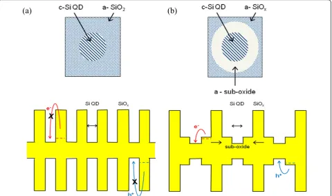
Doping mechanisms for Si QD superlattice structures
As discussed in“Doping and device fabrication for QD nanostructures” section, there is significant evidence for doping on incorporation of B and P in Si QD nanos-tructures from resistivity data and from the formation of rectifying p-n junctions which behave as photovoltaic devices. However, the mechanisms for this doping are not clear. Direct doping of the QDs by impurity atoms is extremely unlikely as the perfectly crystalline nano-crystals segregate any impurity atoms during growth, as shown inab initiocalculations [16,17]. Experimentally, this is supported by data on the free electron density in Si nanocrystals using electron paramagnetic resonance (EPR) [18] which show that at least 95% of P atoms are inactive and segregated to the surface of Si nanocrystals, such that their contribution to doping is at least an
order of magnitude lower than their atomic
concentration.
Another possibility for doping is that the matrix mate-rial, rather than the QDs, is doped by the impurity atoms and that this then provides free carriers which are captured by the QDs. This ‘modulation doping’ mechanism is commonly used in III-V nanostructures. But in III-Vs, the barrier height is typically only a few 100 meV and hence ionisation of dopant atoms is rela-tively easy [9]. In the dielectric matrices used in the Si QD work (particularly for the SiO2barriers), the barrier height is several electronvolts. Under these circum-stances, there would be no ionisation of dopant atoms at room temperature and hence modulation doping could only occur by direct tunnelling of carriers from dopants in SiO2less than 1 nm from the QDs.
If direct doping or doping of a stoichiometric SiO2 matrix are not feasible, then a third possibility is that it is the sub-oxide region surrounding the QDs, as
discussed in “Optical absorption properties of Si nanos-tructures”section and suggested in [12], which is being modulation doped by the P or B dopant atoms. If this region is a sufficiently extended silicon sub-oxide (SiOx),
it could provide flat Bloch bands able to be doped in a pseudo bulk-like regime. If, in addition,x in the sub-oxide is less than about 0.5 (as the data of Figure 3 sug-gests), then the consequent relatively small band gap would allow B and P doping levels shallow enough to be ionised at room temperature. The resultant free elec-trons in the case of P doping (or holes for B doping) would then be available to be captured by the QDs. This would raise (lower) the Fermi level in the QD superlattice and hence create n-type (p-type) material. Alternatively, or perhaps as well, electrons (holes) freed by ionisation could remain in the sub-oxide raising (lowering) its Fermi level and hence directly doping the sub-oxide itself. This modified modulation doping mechanism is illustrated schematically in Figure 5.
This explanation remains a hypothesis at present. More evidence on the exact positioning of dopant atoms is required from techniques such as atom probe tomo-graphy together with direct evidence of doping from EPR.
Conclusions
Quantum confinement in Si QD nanostructures is pro-posed to engineer an increase in the effective band gap and hence produce materials suitable for upper cell ele-ments in a thin-film tandem cell. Si QD materials grown by sputtering alternating Si-rich oxide and stoichio-metric SiO2 layers, with a subsequent anneal to precipi-tate a layered growth of QDs, have been fabricated in previous work. Absorption data on these show a strong absorption region with absorption dependent on Si con-tent and a significant weak absorption tail attributed to sub-oxide regions surrounding QDs due to incomplete diffusion to the growing QDs. Dramatic decreases in resistivity have been demonstrated on incorporation of
Gate contact
Si rich oxide (4nm)
SiO2 (20nm)
SiO2 (2nm)
Quartz substrate
25 bilayers
[image:4.595.66.540.88.193.2](a) (b) (c)
P or B dopants, and rectifying p-n junctions have been fabricated which give a VOC up to 490 mV. However, the mechanism of doping in these materials can neither be direct doping of the QDs nor modulation doping of a stoichiometric SiO2 matrix. A modified modulation doping mechanism is proposed in which P or B atoms dope the sub-oxide region shown to surround QDs, which because of its reduced band gap has dopant levels shallow enough to be ionised and hence provide free carriers to the QDs.
Acknowledgements
This work is supported by the Australian Research Council (ARC) via its Centres of Excellence scheme. The authors also acknowledge the support of the Global Climate and Energy Project (GCEP), administered by Stanford University, for helping to fund this work. The authors also thank all members of the Third Generation Group at the ARC Photovoltaics Centre of Excellence for their contributions to this project.
Authors’contributions
GC worked on the initial concept, on the theory of modified modulation doping and drafted the manuscript. XH carried out the preparation, doping and characterisation of engineered band gap materials; IP fabricated devices and characterised doping and photovoltaic properties; DD participated in the device fabrication and some of the materials preparation; DL fabricated and characterised doped MOS samples. All authors read and approved the final manuscript.
Competing interests
The authors declare that they have no competing interests.
Received: 7 October 2010 Accepted: 21 March 2012 Published: 21 March 2012
References
1. Cho EC, Park S, Hao X, Song D, Conibeer G, Park SC, Green MA:Silicon quantum dot/crystalline silicon solar cells.Nanotechnology2008,
19:245201.
2. Green MA, Conibeer G, Perez-Wurfl I, Huang SJ, Konig D, Song D, Gentle A, Hao XJ, Park SW, Gao F, So YH, Huang Y:Progress with silicon-based tandem cells using group IV quantum dots in a dielectric matrix. Proceedings 23rd European Photovoltaic Solar Energy Conference and Exhibition: September 1-5 2008, Valencia, Spain2008, 1-4.
3. Conibeer G, Green MA, Cho EC, König D, Cho YH, Fangsuwannarak T, Scardera G, Pink E, Huang Y, Puzzer T, Huang S, Song D, Flynn C, Park S, Hao X, Mansfield D:Silicon quantum dot nanostructures for tandem photovoltaic cells.Thin Solid Films2008,516:6748-6756.
4. Perez-Wurfl I, Ma L, Lin D, Hao X, Green MA, Conibeer G:Silicon nanocrystals in an oxide matrix for thin film solar cells with 492 mV open circuit voltage.Solar Energy Materials and Solar Cells2011, 2-5, doi: 10.1016/j.solmat.2011.02.029.
5. Hao XJ, Cho EC, Scardera G, Shen YS, Bellet-Amalric E, Bellet D, Conibeer G, Green MA:Phosphorus-doped silicon quantum dots for all-silicon quantum dot tandem solar cells.Solar Energy Materials and Solar Cells
2009,93:1524-1530.
6. Perez-Wurfl I, Hao XJ, Gentle A, Kim D, Conibeer G, Green MA:Si nanocrystal p-i-n diodes fabricated on quartz substrates for third generation solar cell application.Applied Physics Letters2009,95:153506. 7. Di D, Perez-Wurfl I, Gentle A, Kim DH, Hao X, Shi L, Conibeer G, Green MA:
Impacts of post-metallisation processes on the electrical and
[image:5.595.59.540.90.373.2]
(a)
(b)
photovoltaic properties of Si quantum dot solar cells.Nanoscale Research Letters2010,5:1762-1767.
8. Zacharias M, Heitmann J, Scholz R, Kahler U, Schmidt M:Size-controlled highly luminescent silicon nanocrystals: A SiO/SiO2superlattice approach.Applied Physics Letters2002,80:661.
9. Boer K:Survey of Semiconductor PhysicsNew York: van Nostrand Reinhold; 1990.
10. Jiang CW, Green MA:Silicon quantum dot superlattices: Modeling of energy bands, densities of states, and mobilities for silicon tandem solar cell applications.J Appl Phys2006,99:114902.
11. Hao XJ, Podhorodecki A, Shen YS, Zatryb G, Misiewicz J, Green MA:Effects of Si-rich oxide layer stoichiometry on the structural and optical properties of Si QDs/SiO2multilayer film.Nanotechnology2009,20:485703.
12. Daldosso N, Luppi M, Ossicini S, Degoli E, Magri R, Dalba G, Fornasini P, Grisenti R, Rocca F, Pavesi L, Boninelli S, Priolo F, Spinella C, Iacona F:Role of the interface region on the optoelectronic properties of silicon nanocrystals embedded in SiO2.Physical Review B2003,68:085327.
13. Hao XJ, Cho EC, Flynn C, Shen YS, Park SC, Conibeer G, Green MA:
Synthesis and characterization of boron-doped Si quantum dots for all-Si quantum dot tandem solar cells.Solar Energy Materials & Solar Cells
2009,93:273-279.
14. Lin D, Ma L, Conibeer G, Perez-Wurfl I:Study on electrical properties of Si quantum dots based materials.Physica Status Solidi (B)2011,248:472-476. 15. Conibeer G, Green MA, Koing D, Perez-Wurfl I, Huang SJ, Hao XJ, Di D,
Shi L, Shrestha S, Puthen Veettil B, So Y, Zhang B, Wan ZY:Silicon quantum dot based solar cells: assressing the issues of doping, voltage and current transport.Progress in Photovoltaics: Res Appl2010,18, DOI: 10.1002/pip.1045.
16. Cantele G, Degoli E, Luppi E, Magri R, Ninno D, Iadonisi G, Ossicini S: First-principles study of n- and p-doped silicon nanoclusters.Physical Review B
2005,72:113303.
17. Dalpian GM, Chelikowsky JR:Self-purification in semiconductor nanocrystals.Physical Review Letters2006,96:226802.
18. Stegner AR, Pereira RN, Lechner R, Klein K, Wiggers H, Stutzmann M, Brandt MS:Doping efficiency in freestanding silicon nanocrystals from the gas phase: Phosphorus incorporation and defect-induced compensation.Physical Review B2009,80:165326.
doi:10.1186/1556-276X-7-193
Cite this article as:Conibeeret al.:Si solid-state quantum dot-based materials for tandem solar cells.Nanoscale Research Letters20127:193.
Submit your manuscript to a
journal and benefi t from:
7Convenient online submission 7Rigorous peer review
7Immediate publication on acceptance 7Open access: articles freely available online 7High visibility within the fi eld
7Retaining the copyright to your article
![Figure 3 Room temperature absorption coefficient of annealedThere is a strongly absorbing region at energies above 3 eV, inwhich absorption increases with the Si content of the layers, and aweakly absorbing region at less than 3 eV, which is not stronglySiOx/SiO2 multilayer films with various x (1,100°C, 1 h; [11]).affected by Si content.](https://thumb-us.123doks.com/thumbv2/123dok_us/8854407.936171/3.595.56.290.504.662/temperature-absorption-coefficient-annealedthere-absorption-absorbing-stronglysiox-multilayer.webp)