932
A Multiplier Based Parallel FIR filter
Mr. Abhijit Maidamwar1, Mrs. Swati Sorte2 and Mr. Ketan Machhale3
1 Electronics & Telecommunication , Rajiv Gandhi College of Engineering & Research,
Nagpur, Maharashtra, India
2 Electronics & Telecommunication , Rajiv Gandhi College of Engineering & Research,
Nagpur, Maharashtra, India
3 Electronics & Telecommunication , Rajiv Gandhi College of Engineering & Research,
Nagpur, Maharashtra, India
Abstract —We aim to develop FIR (Finite Impulse
Response) filter using new multiplier that works on dual port memory. The multiplier stores all possible pre-computed product values corresponding to all the possible input multiplicand values. When compared to the distributed architecture processor, this configuration has a reduced memory size and a less number of logic gates. The applications based on digital communication, speech processing make use of this processor. This processor has many other modules incorporated inside it such as 3:8 line address decoder, control circuit, 4bit to 3 bit address encoder, memory, barrel shift register, etc.
This processor is designed and implemented using Hardware Description Language (HDL)
where as to test and verify its functionality, the simulation is done using Xilinx.
Keywords: FIR filter, multiplier
INTRODUCTION
In a variety of applications based on image and signal processing, the FIR filter is used as a basic tool.[1] The width of the transition band is determined by the order of the FIR filter. A sharper transition between a pass band and the adjacent stop band is received with the increase in the order of the filter.[1] There are many applications of signal processing which require that the output of the filter linearly increases with the order of the filter. But real time implementation of these filters of large orders is a very challenging task. Hence a lot of attempts are being made to develop a dedicated VLSI system with reduced complexity for these
933
product length. The designers are in the attempt to reduce the memory space in the DA based architectures by making use of techniques such as offset binary coding and group distributed technique. For implementing an FIR filter a decomposition method has been suggested so that the memory size of a DA based method is reduced but is has been observed that it results in an increase in latency and also the number of adders and latches used. Although a significant study is done and methods have been introduced for efficient look up table multiplier based implementation but any further improvement in the efficiency of look up table multiplier based implementation of FIR filter is not found. We aim to present two approaches for implementation of FIR filters where the size of memory is reduced to half as compared to the conventional method. Also we observe that the transposed form realization of FIR filter’s implementation is more efficient than the direct form.
DESIGN OF LUT FOR MEMORY-BASED MULTIPLICATION
The figure below shows the basic principle used in the memory based multiplication method.
Fig A conventional memory based multiplier
Let us suppose that ‘A’ is a fixed coefficient and ‘X’ is an input word that is to be multiplied with A. If we make an assumption that X is an unsigned binary number of word length L then there are 2 ^L values possible for X and hence there are certain possibilities for the values of the product C which is given by C=A.X . Hence a memory unit of 2L words is required for
implementing the conventional memory based multiplication so that the values can be used as look up table and consist of all the possible pre computed product values of X.
The product word (A.Xi) is stored at the memory location whose address corresponds to the binary value of Xi for 0 ≤ Xi
≤ 2
L-1 in a manner suchthat if the L bit binary value of Xi is used as address for the memory unit then its corresponding product value is read out form memory.
Even if there are 2L values corresponding to the product values of C= A.X , we find that only odd multiples of the corresponding words can be stored in the look up table.
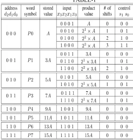
LUT WORDS AND PRODUCT VALUES FOR INPUT LENGTH L = 4
TABLE-1
934
words is found to be zero. The even multiples of A can be obtained by left shifting of one of the odd multiples of A. This has been depicted in the table above which gives the product values for length L=4. The eight odd multiples given by AX (2i+1) are stored as Pi for i=0,1,2,3…….7, at
eight different memory locations. Whereas all the even multiples of A such as 2A, 4A and 8A are obtained by left shifting of A. In the same manner 6A and 12A are obtained by left shifting 3A, and 10A and 14A are obtained by left shifting of 5A and 7A respectively.
The address X=(0000) can be obtained by resetting the output of the look up table. For an input multiplicand of word size L , only the odd values of multiples i.e (2L/2) values are needed to be stored in the core memory of the look up table where as the remaining (2L/2 -1 ) values which are non zero values can be obtained by left shifting of the stored values. Hence a look up table for the multiplication of an L bit input and W bit coefficient can be built on the following assumptions:
1. To store all the multiples of A that are odd, a memory unit of 2L/2 words of (W+L) bit width is needed.
2. To get the even multiples of A , a barrel shifter is required that can produce (L-1) left shifts.
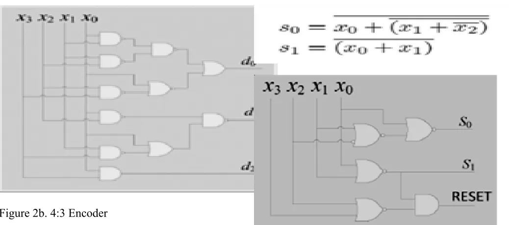
3. An encoder is used to map the input word that is of L bit with the (L-1) bit address of the look up table.
4. For the barrel shifter to produce the required shifts for the output of the look up table the necessary control bits are generated by the control circuit. This control circuit is also responsible for generating a RESET signal which resets the output of look up table when X= 0.
III. Proposed LUT-Based Multiplier for an input of 4-Bit
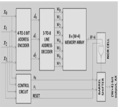
Figure 2 shows the multiplier that is based on look up table for an input of word size L = 4.
Figure 2a. LUT-Based Multiplier for L=4
It consists of a memory array of word length of eight bits (w+4), a 3:8 address decoder, a NOR cell , a barrel shifter, a 4:3 bit encoder which is used to map the 4-bit input operand with the 3-bit address of the look up table, and a control circuit required for generating the control word for barrel shifter as well as the RESET signal for NOR cell.
935
Figure 2b. 4:3 Encoder
The values of AX(2i +1 ) that are pre computed are stored as pi for various values of I from i=0,1,2 ……7 at the eight consecutive memory locations in the memory array. They are shown in table 1in bit inverted form. The decoder takes an address (3 bit ) from encoder input and generates the required word select signals that helps to select the required word from the memory array. The memory array produces an output that is its sub multiple in bit inverted form.
It is clear from table 1 that when then input operand is among one of the values the look up table output is to be shifted left by one location. And if it is (0 1 0 0 ) or ( 1 1 0 0 ) then the shifting is required two times i.e two left shifts are needed. Sometimes three shifts are required whereas for other input operands no shifts are required. As maximum three left shifts are required to taken on a stored word, using a barrel shifter of two stage is sufficient. The number of times the shifting is to be performed on the look up table’s output and that for the control bits for different values are as given in the table 1. Figure 2c. shows the control circuit that generates the control bits which is given by
Figure 2c. Control circuit
Fig 2d. Two-stage logarithmic barrel-shifter for
936
Fig 2 e. Structure of the NOR-cell.
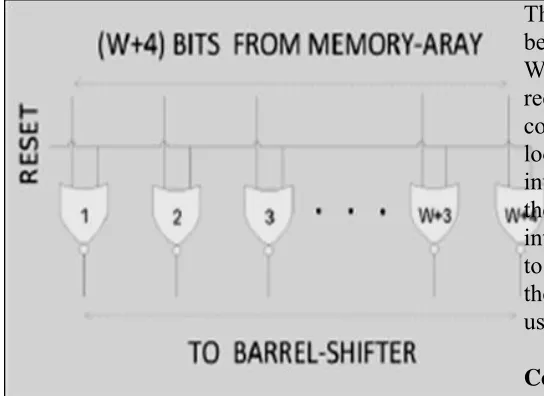
Figure 2d shows a logarithmic barrel-shifter for W=L=4 which consists of two stages of 2:1 line bit level multiplexers with inverted output. In this circuitr each stage consists of (W+4) number of 2 input AND-OR-Invert gates. These AOI gates of first stage feed on the control bits (s0 and ,͞s0) while stage two feeds on (s1 and ,͞s1). Each stage performs multiplexing in an inverted manner hence after two stages the barrel shifter produces the desired number of shifts in an un inverted form.The input X= 0000 corresponds to multiplying by X=0 and gives the product A.X = 0. Hence when the operand value is 0000 , the look up table’s output is be reset which is implemented by a NOR cell as shown in figure 2e. which uses active high reset. The NOR gates receives one input in the form of reset bit and the other input is fed with output of look up table in parallel.
When X=0000 the control circuit generates a RESET signal which is active high and is generated according to the following expression:
The outputs of all the NOR gates are obtained to be 0 when the RESET input is 1.
Whereas when the RESET is 0 the outputs received at the NOR gates becomes complementary to that of the output bits of the look up table. This is the reason why the bit inverted form of the product values is stored in the look up table. All the NOR gates can be integrated with the memory array if the LUT is to be implemented making use of a ROM. Thus the need of NOR cells can be eliminated by using a ROM.
Conclusion
To reduce the size of the look up table as compared to that of the conventional design is the main aim of the design. The size of the look up table is reduced to half by using odd multiple storage for the address length of 4, and by using the components such as a barrel shifter of two stages, (w+4 ) number of NOR gates where w is the length of the word of the multiplying coefficients. For implementation of FIR filter to a further stage the memory based structures having a throughput of unity are to be designed (three numbers). Out of these, one is based on the principle of DA whereas the remaining two are look up table multiplier based making use of both the conventional and the proposed look up table structure.
Acknowledgement
I am really thankful to Mr. P Arudra and the other authors, whose paper helped me a lot to study this
multiplier based parallel FIR filter.
Refrences
937 [3] G. Mirchandani, R. L. Zinser Jr., and J. B. Evans, ―A
new adaptive noise cancellation scheme in the presence of crosstalk [speech signals],IEEE Trans. Circuits Syst. II, Analog Digital Signal Process.
[4] D. Xu and J. Chiu, ―Design of a high-order FIR digital filtering and variable gain ranging seismic data acquisition system,ǁ in Proc. IEEE Southeastcon’93, Apr. 1993, p. 6.
[45 K. K. Parhi, VLSI Digital Signal Procesing Systems: Design and Implementation. New York: Wiley, 1999.
) ( ) ( ) (
1
0 *
N b N r N
b n
m
n
i
n
(1)
Prof. Abhijit Maidamwar M.Tech. (Communication)
Total experience of (8 years) over 5 years in professional teaching field and about 3 years of industrial experience of Software Testing, currently working as Lecturer in Electronics & Telecommunication Engineering at Rajiv Gandhi College of Engineering & Research, Nagpur. He has published 14 papers in various National/International Conference/Journal.
Prof. Swati Sorte M.Tech. (Electronics)
Total 6.5 years of professional teaching experience. Currently working as a lecturer in Rajiv Gandhi College of Engineering & Research,
Prof. Ketan Machhale
M.Tech. (Electronics)