Reshaping Electromagnetic Emissions with Meta-Substrate
Based on Spoof Plasmons
Yao Gao*, Agnes Maurel, and Abdelwaheb Ourir
Abstract—We investigate the efficiency of a metasurface supporting spoof plasmons to control the electromagnetic emission of a radiating element. The three-dimensional metasurface is made of an array of metallic grounded rods, and it is used as the substrate of a printed antenna. Such a substrate provides a transmission band at low frequencies, corresponding to spoof plasmon propagation, and a total electromagnetic band gap above the cut-off frequency. We show how an efficient and directive emission with low side-lobe levels and backward radiation can be obtained when the operating frequency of the antenna is considered in the band gap. The role of the spoof plasmons is further demonstrated by tuning the transmission band at the operating frequency. The proposed meta-substrate is an original and efficient alternative to reshape the emission of electromagnetic sources.
1. INTRODUCTION
Electromagnetic radiating sources involve planar structures susceptible to support surface waves. These waves, bounded to the interface, propagate, and when they reach edges or corners, they diffract in free space. This mechanism is used as the main radiating mechanism in the travelling-wave antennas (or leaky-wave antennas) based on the design of a guiding structure that can efficiently couple the surface waves to free space. It is in contrast to resonant antennas, which use resonances of radiating elements (as monopoles or dipoles). However, even in this case, surface waves are involved but in an undesirable way. Indeed, such antennas are mounted over a larger plane surface (the ground plane), which is susceptible to support surface waves, as surface plasmons for metallic ground plane in the optical frequencies. The antennas are designed by considering an infinite ground plane ignoring surface wave radiation. Because of the finite size of the ground plate in the practice, the surface waves are scattered, and thus, interact with the field of the radiating elements. It results in the appearance of undesired ripples and high level side lobes in the radiation pattern, responsible for a decrease in the overall performances of the antenna. To avoid such perturbations, one has to prevent the wave propagation on the ground plane. This means that the surface waves have to be associated to a dispersion relation with frequency ranges where the propagation is prevented, namely with band gaps.
In 1999, two designs of improved antennas were proposed [1, 2], where the planar interface of the ground plane is replaced by a periodically structured interface. In the former reference [1], the structure consists in piercing a square array of air columns in a dielectric substrate. The array at wavelength scale realizes a photonic crystal type substrate, which present a forbidden band gap at the Bragg frequency. In a latter reference [2], the forbidden frequency band is realized using a mushroom-like array designed at a subwavelength scale. The concept of surface impedances is used to characterize the response of the structure, resulting in the so-called high impedance surfaces, associated with forbidden frequencies for the surface waves. The effect of the excitation of surface waves on radiating elements has been studied in many contexts [3, 4]. Recently, a microstrip patch antenna array and a beam-scanning
Received 2 March 2016, Accepted 6 June 2016, Scheduled 6 July 2016
* Corresponding author: Yao Gao ([email protected]).
frequency). Note that the restriction to tankL >0 is not mentioned in [8–10] although it is essential to define the band gaps, and it can be obtained by using classical homogenization technique [11, 12]. The wavefield in air isH(x, z) =H0eikSPx−αz, withk2 =kSP2 −α
2. The forbidden frequency ranges correspond
to negative values of tankL, leading to the usual first total band gap, which is forπ/2L≤k≤π/L[12]. In the following, we refer to the forbidden frequency range, the corresponding range of frequencyf such thatc/4L≤f ≤c/2L, withc= 3.108m·s−1.
In the context of the improved antenna, the existence of stop bands is interpreted in terms of high impedance surface (HIS) [2], with the surface impedance Zs = Ex/H with our notations. Being the ratio of two conserved quantities,Zsis notably continuous at the interfacez= 0 between the corrugated layer and air. Thus, if Zs(0−) is known, one can solve the problem only in the air (z ≥ 0) using the boundary condition at the equivalent surfacez= 0 (obviously, the difficulty is to find preciseZs, which requires to solve the problem forz <0). In our two dimensional configurations,Zsimposes a boundary condition of Robin type ∂zH(x= 0, z) =iωZsH(x= 0, z) (since ∂zH=iωEx when considering a time dependencee−iωt). When looking surface waves,H(x, z >0) =H0eikSPx−αz, we simply getα=−iωZs.
This means that surface waves (withαreal positive) will be supported forZshaving a positive imaginary part (inductive impedance). Next, if Zs tends to infinity, α and kSP = k2+α2 also tend to infinity, which indeed coincides with the limits of the stop bands in our case, Eq. (1), at tankL→ ±∞.
In the following, we use the concept of plasmon band gap (given by the condition tankL <0 in Eq. (1)) to design our metamaterial substrate, and we experimentally and numerically demonstrate its capability of improving the performances of patch antenna.
2. TOTAL SPOOF PLASMONS BAND GAP IN A TWO DIMENSIONAL METAMATERIAL
Let us start by considering the simplest structure (one dimensional case) with rectangular grooves and parameters ϕa = 6 mm and a = 13 mm. Two different groove lengths, L = 6 and L = 15 mm, are considered. Fig. 1(a) shows the corresponding dispersion relations given by Eq. (1). The light line that corresponds to the dispersion relation in vacuum is also given for comparison. Spoof plasmon modes are clearly observed over a wide band at low frequencies for both structures. A band gap is obtained in each geometry and can be easily tuned by the groove length.
It has been shown recently that the dispersion relation of surface waves in ultrathin and flexible films is practically identical to the relation provided by corrugated surfaces [13, 14]. Here, we propose to take advantage of this phenomenon to go toward a two-dimensional structure. For practical consideration, we use the two-dimensional configuration illustrated in Fig. 1(b). Instead of massive rectangular grooves invariant along y, we consider cylindrical rods periodically located along x and y with the same parameters (a, L) and 2R=ϕa.
(a)
(c)
(b)
Figure 1. (a) Schematic view and dispersion diagram of a corrugated surface (factor ϕ = 0.46 and a= 13 mm) for two different groove lengths. (b) Schematic view of the metamaterial made of an array of grounded rods. (c) Dispersion diagram of the proposed metamaterial calculated for two different cylinder lengths. The light line is plotted as well (dotted line).
f = 8.5 GHz. The proposed two-dimensional metamaterial supports the propagation of spoof plasmon modes ruled by a dispersion relation that can be tuned by the length of the rods as predicted by Eq. (1).
3. RESHAPING THE RADIATION PATTERN
At microwave frequencies, patch antennas are the most common radiating sources employed in integrated circuits that play the important role of emitting signals off the chip into free space. As already mentioned, these patch antennas are placed on a dielectric substrate over a metallic ground plane, which can support surface waves and couples power into substrate modes. The diffraction of these waves at the edges of the substrate affects the antenna efficiency and causes ripples and high level side lobes in the radiation pattern. We now inspect the ability of our metamaterial substrate to avoid such unpleasant effects by preventing surface wave, or spoof plasmon, propagation.
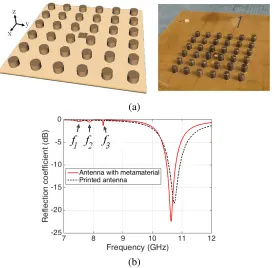
We realize a patch antenna resonating around 10 GHz. The width of the radiating patch is 6 mm, and its length is 5.8 mm. It is fed by a coax cable line via a hole near the center of the ground plane. The antenna element is then placed in the center of a 6 by 6 cylinder array with L= 6 mm, as shown in Fig. 2(a) (and from Fig. 1(c), we know that this structure provides a band gap that surrounds the resonant frequency of the antenna even after adding the thin layer of the epoxy substrate).
(b)
Figure 2. (a) Schematic view and a photography of the printed antenna surrounded by the metamaterial structure. (b) Reflection coefficients calculated for the antenna with and without the metamaterial (f1= 7.75 GHz,f2= 7.87 GHz and f3 = 8.34 GHz).
that the resonant frequencies, f1 = 7.75 GHz, f2 = 7.87 GHz and f3 = 8.34 GHz, are very weak in the
present case; additional results on these low frequency resonances are reported in the last section, where we show that the structure can be optimized to work efficiently at these frequencies [15–17].
The radiating patterns have been measured in a semi-anechoic chamber using a network analyser. The measurements have been performed at the main resonance,f = 10.6 GHz, in theEandHplanes for the realized antenna. The results are presented in Fig. 3. A significant enhancement of the directivity of the antenna is achieved due to the metamaterial substrate. A reduction of the backward radiation and side-lobe levels, in particular for angles higher than 90 degrees, is also obtained on the two planes. An average value of reduction of 10 dB is observed. Moreover, the gain of the antenna is increased about 2 dB at the operating frequency. This improvement is higher (of about 1 dB) than the one obtained with photonic crystals (PCs) and high impedance surfaces (HISs) when considering similar lateral dimensions. In order to further investigate the role of the band structure on the radiation patterns, we consider a second metamaterial for which the spoof plasmon propagation is possible at the operating frequency (f0 10 GHz) of the printed antenna [see Fig. 1(c)]. This is done by considering a metamaterial
(a) (b)
Figure 3. (a) Measured and simulated radiation patterns in theE plane for the antenna alone and the antenna surrounded by the metamaterial surface. (b) Same representation as in (a) for the measurements in theH plane.
(a)
(c) (b)
Figure 4. (a) Reflection coefficients of the antenna in the absence and in the presence of the metamaterial surface. (b) and (c) Radiation patterns of the printed antenna surrounded by the metamaterial measured respectively in theE plane and in the H plane.
4. ELECTROMAGNETIC RADIATION FROM THE FINITE SIZE METAMATERIAL
(c) (b)
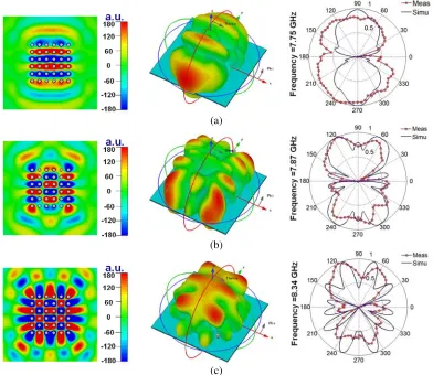
Figure 5. Electric field distribution (left) and radiation patterns (center for 3D and right for 2D patterns) calculated at the resonant mode frequencies: (a) f1 = 7.75 GHz, (b) f2 = 7.87 GHz and (c)
f3 = 8.34 GHz. The frequencies are defined in Fig. 2. Measurements are also given for the in-plane 2D
patterns.
While we studied the behavior of the structure at the main resonance, we have not investigated the collection of resonant peaks observed at the lower frequencies of the reflection spectrum presented in Fig. 2(b). We propose now to focus on this phenomenon.
It appears that such a reflection coefficient response was recently observed in a finite size structure called metalens [15–17]. This structure consists of a finite size periodic array of sub-wavelength resonators. The formalisms used to study this type of resonant media have shown that the coupling splits the single resonance of the atom, considered in each unit cell, to different modes shown at different frequencies. This hybridization process produces a number of modes, which at best equals the number of unit cells. However, due to mode overlapping and symmetries, it is not always possible to individually excite each of these modes.
While designed to mimic corrugated surfaces in order to support spoof SPs in a two-dimensional configuration, our metamaterial can be considered as a cluster of a resonant grounded rods disposed periodically according to a two-dimensional square lattice. This overview incites us to consider this structure as a metalens and predict the appearance of the collection of resonant modes presented in Fig. 2(b).
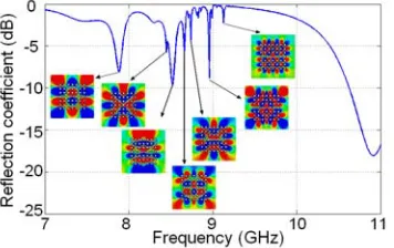
Figure 6. Radiation pattern and magnetic field distribution on plane.
metamaterial. In order to take a closer look in the near-field variations at these resonant frequencies, we have performed numerical simulations. Fig. 5 shows the cartography of the electric field variation above the structure at the three main resonant frequencies. The spatial fluctuations on the near-field patterns is related to the Fabry-Perot resonant behavior of the structure. These modes can be expressed in terms of in-plane wavenumber ksp = πa(mx+ny), where m and n are integers inferior or equal receptively to the number of the columns and lines of the considered array, wherea is the lattice constant of the array.
These results match the metalens behavior presented above [17]. Thereby, we expect a far-field radiation in the plane of the structure with a specific pattern at each resonant frequency. We have performed calculations and measurements in order to characterize the radiation patterns. Fig. 5 shows the results at the three main considered frequencies, 7.75 GHz, 7.87 GHz and 8.34 GHz, respectively. We can notice that each pattern expresses the fluctuation observed in the corresponding near-field resonant mode.
The resonant modes obtained here by hybridization do not present resonances with high magnitude because the coupling of the structure to the main source (patch antenna) has not been optimized here to that aim. In Fig. 6, we present the spectrum obtained with a configuration where such coupling is amplified. In such a configuration, efficient radiation at each resonance and a wide diversity of radiation patterns can be obtained. This structure can be used as an original and efficient solution to reshape the radiation pattern for specific configurations.
5. CONCLUSION
In this work, we have realized a meta-substrate made of a finite array of grounded metallic rods realizing a transmission band for surface waves at low frequencies and a total electromagnetic band gap above a specific cut-off frequency. This meta-substrate has been shown to efficiently reshape the radiated field of a printed antenna, and the role of the band structure has been illustrated. Finally, for operating frequency in the transmission band, one can reshape the radiation pattern in a different way, for instance to realize additional lobes, as observed in our second experiments at−45, 0 and 45 degrees. Given the analogy between acoustic and electromagnetic waves [18, 19], our concept could be extended to acoustics by using analogous sonic crystals or sound-hard inclusions.
ACKNOWLEDGMENT
This work is supported by LABEX WIFI (Laboratory of Excellence within the French Program “Investments for the Future”) under references ANR-10-LABX-24 and ANR-10-IDEX-0001-02 PSL*.
REFERENCES
scanning circularly polarized patch array,”Journal of Physics D: Applied Physics, Vol. 47, No. 32, 325101, 2014.
7. Yang, F. and Y. Rahmat-Samii, Electromagnetic Band Gap Structures in Antenna Engineering, Cambridge University Press, 2009.
8. Kelders, L., J. F. Allard, and W. Lauriks, “Ultrasonic surface waves above rectangular-groove gratings,” Acoustical Society of America Journal, Vol. 103, 2730–2733, May 1998.
9. Pendry, J. B., L. Martn-Moreno, and F. J. Garcia-Vidal, “Mimicking surface plasmons with structured surfaces,” Science, Vol. 305, No. 5685, 847–848, 2004.
10. Garcia-Vidal, F. J., L. Martn-Moreno, and J. B. Pendry, “Surfaces with holes in them: New plasmonic metamaterials,” Journal of Optics A: Pure and Applied Optics, Vol. 7, No. 2, S97, 2005. 11. Maurel, A., S. Flix, J.-F. Mercier, and A. Ourir, “Effective birefringence to analyze sound transmission through a layer with subwavelength slits,” Comptes Rendus Mcanique, Vol. 343, No. 12, 612–621, 2015 (Acoustic metamaterials and phononic crystals).
12. Mercier, J.-F., M. L. Cordero, S. F´elix, A. Ourir, and A. Maurel, “Classical homogenization to analyse the dispersion relations of spoof plasmons with geometrical and compositional effects,”
Proceedings of the Royal Society of London A: Mathematical, Physical and Engineering Sciences, Vol. 471, No. 2182, 2015.
13. Shen, X., T. J. Cui, D. Martin-Cano, and F. J. Garcia-Vidal, “Conformal surface plasmons propagating on ultrathin and flexible films,” Proceedings of the National Academy of Sciences, Vol. 110, No. 1, 40–45, 2013.
14. Cano, D., M. L. Nesterov, A. I. Fernandez-Dominguez, F. J. Garcia-Vidal, L. Martin-Moreno, and E. Martin-Moreno, “Domino plasmons for subwavelengthterahertz circuitry,” Opt. Express, Vol. 18, 754–764, Jan. 2010.
15. Lemoult, F., G. Lerosey, J. de Rosny, and M. Fink, “Resonant metalenses for breaking the diffraction barrier,”Phys. Rev. Lett., Vol. 104, 203901, May 2010.
16. Ourir, A., G. Lerosey, F. Lemoult, M. Fink, and J. de Rosny, “Far field subwavelength imaging of magnetic patterns,”Applied Physics Letters, Vol. 101, No. 11, 111102, 2012.
17. Jouveaud, C., A. Ourir, and J. Rosny, “Surface waves radiation by finite arrays of magnetoelectric resonators,”Progress In Electromagnetics Research, Vol. 132, 177–198, 2012.
18. Mercier, J.-F., M. L. Cordero, S. F´elix, A. Ourir, and A. Maurel, “Classical homogenization to analyse the dispersion relations of spoof plasmons with geometrical and compositional effects,”
Proceedings of the Royal Society of London A: Mathematical, Physical and Engineering Sciences, Vol. 471, No. 2182, 2015.