Black-Si as photoelectrode
Denver P. Linklater1,2,3∗, Fatima Haydous4,5, Cheng Xi4, Daniele Pergolesi4, Jingwen Hu3, Elena P. Ivanova1, Saulius Juodkazis3,6, Thomas Lippert4, Jurga Juodkazyt˙e7
1 School of Science, RMIT University, Melbourne, VIC 3000, Australia
2 Melbourne Centre for Nanofabrication, ANFF, 151 Wellington Road, Clayton, VIC 3168, Australia
3 Optical Sciences Centre and ARC Training Centre in Surface Engineering for Advanced Materials (SEAM), School of Science, Swinburne University of Technology, Hawthorn, VIC 3122, Australia
4 Laboratory for Multiscale Materials Experiments, Paul Scherrer Institut, CH-5232 Villigen PSI, Switzerland 6 Tokyo Tech World Research Hub Initiative (WRHI), School of Materials and Chemical Technology, Tokyo
Institute of Technology, 2-12-1, Ookayama, Meguro-ku, Tokyo 152-8550, Japan
7 Center for Physical Sciences and Technology, Saul ˙etekio ave. 3, LT-10257 Vilnius, Lithuania
* Correspondence: (D.L.) [email protected]; (T. L.) [email protected]; (J. J.) [email protected]
† Current address:5KTH Royal Institute of Technology, Division of Applied Physical Chemistry, Teknikringen 30, SE-114 28, Stockholm, Sweden
Received: date; Accepted: date; Published: date
Abstract:The fabrication and characterisation of photo-anodes based on black-Si (b-Si) is presented using a photo-electrochemical cell in NaOH solution. Black-Si was fabricated by maskless dry plasma etching and was conformally coated by tens-of-nm of TiO2using atomic layer deposition (ALD) with
a top layer of CoOxcocatalyst deposited by pulsed laser deposition (PLD). Low reflectivityR<5% of
Black-Si over the entire visible and near-IR (λ<2µm) spectral range is favorable in better absorption
of light while an increased surface area facilities larger current densities. Photoelectrochemical performance of the heterostructured photoanode is discussed in terms of n-n junction between b-Si and TiO2.
Keywords:black Si; antireflection; photo-anode; water splitting
1. Introduction
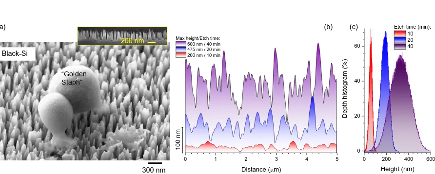
Nanotextured silicon - Black-Si [1] - has a range of useful properties: it acts as an antireflection surface over the vis-IR spectral range, has bactericidal activity against gram positive and negative bacteria [2] (Fig.1(a)), can rupture soft membranes of red blood cells [3], can act as a field emitter electrode [4], can be rendered into a hydrophobic surface, substrates for surface enhanced Raman sensors/spectroscopy (SERS) [5] and it is used for solar cells [6,7]. Recently, optical binding/trapping of Black-Si was demonstrated at very high laser powers when nonlinear optical effects inside trapped material can be induced [8]. High thermal conductivity of Black-Si due to its crystalline nature is a useful property in heat dissipation also helped by the larger surface area of Black-Si. This wide range of applications are enabled by the specific physico-chemical properties of the nanostructured silicon surface. Black-Si surface topography presents with a random array of high aspect ratio spikes that can efficiently trap light (enhance absorption and reflection since reflection is suppressed), due to gradual refractive index change.
There is increasing interest to use black-Si as a photoelectrode in photelectrochemical (PEC) splitting of water as both a photoanode and photocathode. Nanoporous p-type b-Si with a hybrid organic/inorganic interfacial architecture, consisting of organic molecular monolayer beneath ALD-deposited TiO2modified with Pt nanoparticles (NPs), was recently studied as a photocathode [9].
The critical importance of careful consideration of semiconductor junction engineering was pinpointed. Yang et al. (2019) [10], introduced a dual protection layer strategy where the first layer of TiO2
was ALD deposited on p-type nanoporous Black-Si, while the second layer was deposited on top
0 200 400 600 0
20 40 60
Etch time (min): 10 20 40
Dept
h h
istog
ra
m (
%)
Height (nm)
0 1 2 3 4 5
Distance (mm) Max height/Etch time:
600 nm / 40 min 475 nm / 20 min 200 nm / 10 min
10
0 n
m
300 nm Black-Si
“Golden Staph”
200 nm
(a) (b) (c)
Figure 1.Mechanically bactericidal surface of Black-Si. (a) SEM image of a Gram-positiveStaphylococcus
aureus“Golden Staph” cell ruptured on b-Si. Inset shows SEM side-view image of Black-Si prepared by typical 15 min dry plasma etching with SF6and O2gases. (b) Height profiles of AFM cross sections for different plasma dry etching times of 10, 20 and 40 min. (c) Depth histogram: a depth (height) pixel distribution in the AFM image of Black-Si etched for different times (see Appendix for the bearing ratios and statistical analysis).
of the hydrogen evolution reaction (HER) cocatalyst. Significant improvement in the durability of Black-Si photocathodes in both acid and alkaline medium was demonstrated. Contrary to these results, Oh et al., (2019) [11] reported that transition metal NPs electrodeposited directly on n-type Black-Si surface can stabilize photoanodes without the need for a protection layer. However, the role of protective layer in their study was, in fact, played by thermally grown SiOx. Recently, Black-Si
demonstrated enhanced photoelectrochemical efficiency and stability using a conformal TiO2film on a
nanoporous n-type silicon photoanode [12]. This b – Si/TiO2/Co(OH)2nanostructured photoelectrode
produced a saturated photocurrent density of 32.3 mA.cm−2at an external potential of 1.48 V versus reference reference electrode (RHE) in 1 M NaOH electrolyte under 1 Sun illumination. The authors demonstrated that amorphous ALD TiO2layer was able to passivate defective surface sites, increase
the efficiency of electron-hole separation as well as lifetime of minority charge carriers in n-type Black-Si PEC photoelectrodes.
Here, Black-Si surfaces were assessed for their photoelectrochemical (PEC) performance by exploring the influence of surface spike topography (height/pitch) and TiO2film thickness. A layer
of CoOxas oxygen evolution reaction (OER) cocatalyst was explored to enhance the photo-current
output.
2. Experimental
Fabrication of photo-anodes.Black-Si was fabricated using n-type As-doped 100 mm diameter silicon wafers with specific resistivity of 0.005Ω.cm and processed with a Samco RIE101iPH inductively coupled plasma (ICP) assisted reactive ion etching (RIE) tool. Silicon surfaces were initially cleaned with isopropanol and then dried under nitrogen gas flow to remove contaminants. Silicon wafers were then etched according to the following recipe: the etchant gases were SF6/O2with respective flow rates
535 530 525 1 2 3 4 5 Counts (10 4)
Binding energy (eV)
460 455 450
0 1 2 3 4 Counts (10 4)
Binding energy (eV)
1000 800 600 400 200 0
0 10 20
Counts (10
4 )
Binding energy (eV)
(b) (c) (d)
100 nm
10 nm TiO2 25 nm TiO2 50 nm TiO2
(a)
Black-Si
Ti
LMN O KLL Ti
2s O 1s Ti 2p Si 2p C 1 s O 1s Ti -OH 5 28 eV Ti -O 52 6 eV Ti 2p
Ti4+ 2p ½ 461 eV
Ti4+ 2p 3/2
456 eV
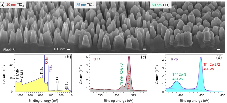
Figure 2.Surface characterisation of Black-Si photoelectrodes. (a) Side-view SEM images of Black-Si
coated with different thickness of TiO2by atomic layer deposition (ALD). Scale bars 100 nm. Black-Si was etched for 40 min. (b-d) XPS surface analysis for wide and narrow spectral windows at O1s and Ti2p bands from sample coated with 25 nm of TiO2.
TiO2thin films of 10, 25 or 50 nm were deposited using atomic layer deposition (ALD) (Cambridge
Nanotech ALD Fiji F200 & Savannah s100). Black-Si samples were used for the ALD coating without removal of native oxide. Figure2shows SEM images and X-ray photo-electron spectroscopy (XPS) characterisaiton of the surfaces after TiO2 deposition. A cobalt oxide CoOx cocatalyst layer was
deposited using pulsed laser deposition (PLD) setup based on a 248 nm wavelength KrF eximer laser [13]; PLD is a practical method to deposit materials from targets with complex composition at fast deposition rate. Surface morphology was inspected by SEM.
PEC Measurements.PEC measurements were performed in a three-electrode configuration in 0.5 M NaOH (pH 13.0) aqueous solution. The b-Si photoelectrode was used as the working electrode. Silver paste was applied for the electrical connection between the sample and the clamped wire; an epoxy resin covered the contact and insulated it from the electrolyte. Epoxy resin was also used to insulate the back side and the edges of the b-Si sample to avoid electrical short-circuit with only the front side of the sample exposed to the electrolyte and light. A coiled Pt wire and Ag/AgCl were used as the counter and reference electrodes, respectively. To simplify the display of the working electrode potential, the potential versus reference hydrogen electrode (RHE), obtained according to the relation E(vs RHE) = E(vs Ag/AgCl) + 0.197 + 0.059pH, has been adopted throughout this article. A Solartron 1286 electrochemical interface was used to carry out the voltage scan and current collection. Potentiodynamic measurements with a scan rate of 10 mV/s in the potential window of 0.5 - 1.7 V RHE were performed to investigate the PEC performance of b-Si-TiO2multiphases. The chopped
dark-light current densities were normalized according to the illuminated area. The light source was a 150 W Xe lamp equipped with an AM 1.5G filter (100 mW/cm2, Newport 66477-150XF-R1) calibrated with a photodetector (Gentec-EO).
3. Results and Discussion
states of Si [17]. In basic solutions, Si is usually stable at room temperature [18], hence, is promising as an electrode. When metals or semiconductors are deposited over Black-Si surfaces, a light scattering pattern creates de-polarisation of light and the E-field component perpendicular to the electrode or catalyst surface could be formed and facilitate a charge (electron or hole) transport through the interface [19].
3.1. Black-Si with TiO2: potentiostatic and potentiodynamic scans
0.2 0.4 0.6 0.8 1.0 1.2 1.4 1.6 -0.02 -0.01 0.00 0.01 0.02 0.03 0.04 0.05
E vs RHE (V) 0.0 0.2 0.4 0.6 0.8 1.0 1.2 1.4 1.6
-0.02 -0.01 0.00 0.01 0.02 0.03 0.04 0.05
E vs RHE (V) 0.2 0.4 0.6 0.8 1.0
-0.01 0.00 0.01 0.02 0.03 Curr ent I ( mA/cm 2)
E vs RHE (V)
(a) (b) (c)
b-Si 10 min TiO2 [nm]:
0, 10, 25, 50
b-Si 20 min TiO2 [nm]:
10, 25, 50
b-Si 40 min TiO2 [nm]:
10, 25, 50
LightON OFF
dark current
photocurrent
Figure 3.Potentiodynamic scans for the Black-Si photoanodes fabricated for 10, 20 and 40 min and
coated with 10, 25, or 50 nm TiO2, respectively in NaOH electrolyte under chopped light illumination; x,y-scales are different for a better presentation.
0 10 20 30 40 50
0.00 0.01 0.02 0.03
Time (s)
0 10 20 30 40 50
0.00 0.01 0.02 0.03
Time (s)
0 10 20 30 40 50
0.00 0.01 0.02 0.03 Curr ent I ( mA/cm 2) Time (s)
(a) (b) (c)
b-Si 10 min TiO2 [nm]: 0, 10, 25, 50
b-Si 20 min TiO2 [nm]:
10, 25, 50
b-Si 40 min TiO2 [nm]:
10, 25, 50
ON OFF L ig h t
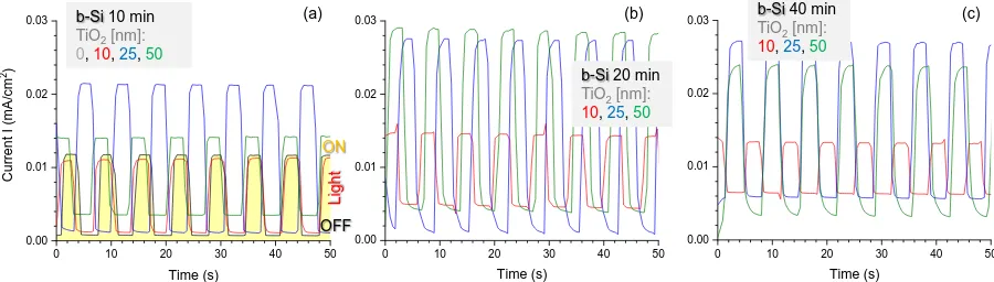
Figure 4.Potentiostatic scan at 1.23 V vs RHE for the Black-Si photoanodes fabricated for 10, 20 and
40 min and coated with 10, 25, or 50 nm TiO2, respectively in NaOH electrolyte under chopped light illumination.
Potentiodynamic polarization curves recorded in the solution of 0.5 M NaOH under chopped illumination for b-Si electrodes fabricated using different etching times and coated with TiO2layers of
different thickness are compared in Fig.3. A slight increase in the magnitude of dark currents with increase in etching duration can be observed in Figs.3(a-c). This can be attributed to the increase in electrochemically active surface area of the electrode with etching time, which is consistent with the height profiles of AFM cross-sections shown in Fig.1(b). Another observation is that the deposition of TiO2on Black-Si leads to an increase in photoanodic current. This is especially obvious in the
case of Black-Si samples with higher roughness, i.e., etched for 20 and 40 min. The most significant effect of TiO2on the photocurrent is observed when its thickness increases from 10 nm to 25 nm,
whereas further thickening of the layer up to 50 nm was not efficient in terms of photoelectrochemical performance of the samples.
TiO2 n-Si
visible
UV
+ EF
Ec
Ev
Ele
ctron
en
erg
y,
eV
eV
b
ias
Ele
ctrod
e
10-50 nm Black-Si
h e
(a) (b)
el
ectro
ly
te
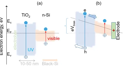
Figure 5.Band diagram of n-n junction between Si and TiO2without (a) and with (b) bias. Black-Si
was made on n-type Si. Under positive bias, holes are drifting to the titania-solution interface while electrons are drawn into the electrode bulk. Bandgap of TiO2is 3.1 eV (400 nm) and 1.12 eV for Si. Under a white light (spectrally broad) illumination, e-h generation occurs at the both materials forming a TiO2-Si n-n-junction. Arrows show e,h drift direction.
etched for 20 min with 25 nm thick TiO2layer (Fig.4(b)), which means that such fabrication conditions
ensure the most efficient generation, separation and transport of the charge carriers. To analyze these processes in more detail, energy band diagram of n-n junction between n-type Black-Si and n-type TiO2has been constructed and is shown in Fig.5. These semiconductors form type-I, or straddling
gap, heterojunction. In accordance with the their bandgap values, i.e. 3.1 eV for TiO2and 1.12 eV
for Si, titania will absorb UV portion of incident light, while silicon will absorb longer wavelengths. In the case of a n-type photoanode immersed into electrolyte solution under illumination (white light), photogenerated holes should be drifting to semiconductor-electrolyte interface to participate in the oxidation of solution species (water molecules), whereas photoelectrons should be driven to the electrode bulk and towards counter electrode to take part in the reduction reaction. Due to upward band bending at the hetrojunction between the two n-type semiconductors, an energy barrier is formed for the transport of photo-generated electrons from the conduction band of TiO2to that of Si (Fig.5(a)
at no external bias conditions. The barrier for photoholes drifting from the valence band of Si to the valence band ofTiO2is even higher. Positive polarization of the electrode provides the energy required
to overcome this barrier (Fig.5(b)) and this is the reason why photocurrent increases with increase in electrode potential as can be seen in Fig.3.
The surface area increase with etching timetcan be evaluated from the height evolution of the Black-Si pyramids ash(t)[15]. Side walls of pyramids has∼6◦angle with the normal to the initial flat surface of Si. The surface area of b-Si can be estimated from a scaling argument by measuring the side-lengthx(t)2wherexis measured from a side-view of b-Si cross section (inset in Fig.1(a)). A linear evolution of the height wash(t)∝4.5×h(15 min). The x-length of cross-section aftert1 =15 min
etching was increasingx(15 min)/x(0 min)≈3.96 times, hence the area increase wasx2∝15.7 times.
For longer etching timesx(h)2∝ph/h(t1)x(t1)2, wheret1=15 min. After 45 nm etching,h=900 nm
tall pyramids of Black-Si are fromed [15] and the surface area was approximately 30 times larger as compared the initial flat surface of Si.
3.2. Black-Si with TiO2and CoOx: potentiostatic and potentiodynamic scans
Semiconductor modification with oxygen/hydrogen evolution (OER/HER) cocatalysts is a common strategy to increase the efficiency of photoelectrochemical water splitting reactions [20]. In this study 150 nm thick layer of cobalt oxide CoOxwas deposited on b-Si fabricated for 20 min
and coated with 10 nm TiO2. The surface morphology of as-fabricated sample is shown in Fig.6.
1 µm 200 nm Black - Si
Si
CoOx
Figure 6.SEM images of as-fabricated Black-Si photoanodes etched for 20 min and coated with 10 nm
TiO2with addition of 150 nm CoOxcocatalyst.
0.00 0.25 0.50 0.75 1.00 1.25 1.50 -0.02
0.00 0.02 0.04 0.06 0.08 0.10
Curr
en
t d
en
sity (m
A.cm
-2)
Potential E vs RHE (V)
Planar Si/TiO2(10nm)
b-Si (20min)/TiO2(10nm)
b-Si (40min)/TiO2(10nm)
b-Si (20min)/TiO2(10nm)/CoOx(150nm)
0 50 100 150 200
0.00 0.01 0.02 0.03 0.04
Curr
en
t d
en
sity (m
A.cm
-2)
Time (s)
Planar Si/TiO2(10nm)
b-Si (20min)/TiO2(10nm)
b-Si (40min)/TiO2(10nm)
b-Si (20min)/TiO2(10nm)/CoOx(150nm)
(a) (b)
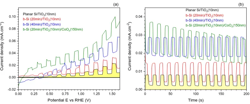
Figure 7.Potentiodynamic (a) and potentiostatic (b) scan at 1.23 V vs RHE for the Black-Si photoanodes
fabricated for 20 and 40 min and coated with 10 nm TiO2with addition of 150 nm CoOxcocatalyst layer in NaOH electrolyte under chopped light illumination. The potential scan speed was 10 mV/s and light ON-OFF chopping with∼8 s period in (a).
that fabrication conditions adopted in this study for the formation of heterostructured photoelectrode allowed to preserve the initial morphology of Black-Si substrate, contrary to the case reported in ref. [12], where top layer of Co(OH)2was electrodeposited on b-Si/TiO2(8 nm) blocking large areas of
underlying substrate underneath a thick coating.
The results of PEC investigations are summarized in Fig.7and compared with the response of planar Si photoelectrode with 10 nm TiO2coating as well as that of Black-Si fabricated for 40 min with
10 nm TiO2. The increase in both dark- and photo-currents in the sequence: planar Si/TiO2(10 nm)
< b-Si(20 min)/TiO2(10 nm) < Black-Si(40 min)/TiO2(10 nm) should be attributed to an increase in
electrochemically active surface area of the electrode (Fig.7(a)). It should be noted, however, that an increase in dark currents is more pronounced than that of photocurrents (taken as difference between the current values in dark and under illumination). Moreover, the increase in both dark- and photo-currents of planar-Si vs Black-Si is not comparable with increase in surface area of the samples (about 30 times) as discussed above. A possible explanation to this could be the mentioned energy barrier, which forms at the heterojunction between n-type Si and TiO2(Fig.5). Deposition of CoOxleads to
significant increase in photocurrents, especially in the range of lower potential values, i.e. 0.1 V <E < 1.1 V. This can be attributed to efficient hole-mediated oxidation of water molecules to O2on the
surface of cobalt oxide cocatalyst.
1 µm 200 nm 20 µm
CoOx
Black - Si NaOH immersed
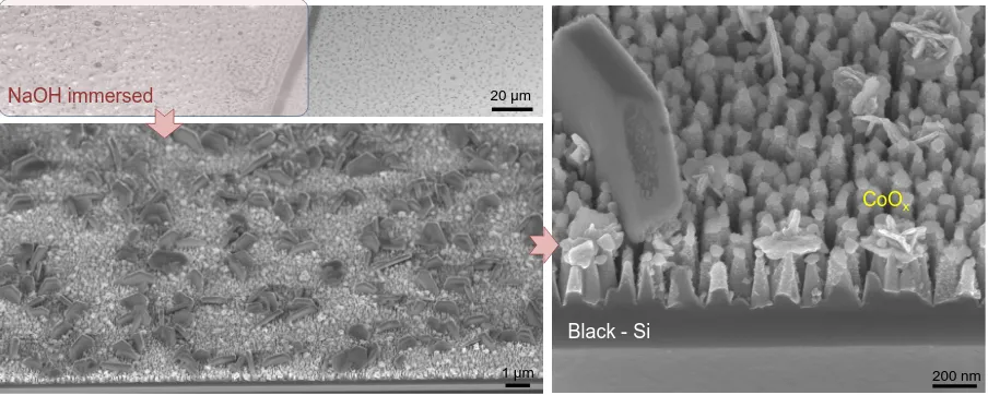
Figure 8.SEM images of Black-Si photoanodes etched for 20 min and coated with 10 nm TiO2with
addition of 150 nm CoOxcocatalyst after the exploitation for 30 min in photoelectrochemical cell.
1.23 V. This points to some rearrangement of the photoactive layer. SEM images of the photoelectrode made after the OER-exploitation in PEC cell for 30 min in NaOH electrolyte (Fig.8) reveal drastic changes in the morphology of the sample with sub-micrometer sized hexagonal crystals randomly distributed all over the surface. Such morphology is characteristic to CoOOH [21], which is known to play the role of active site in oxygen evolution reaction [22].
The mechanism of photoelectrocatalytic OER on the surface of CoOx-modified
b-Si(20 min)/TiO2(10 nm) could be as follows. Holes photogenerated in B-Si/TiO2 drift to
the electrode/solution interface, where they are captured by CoOx. This interaction leads to
oxidation of active cobalt oxide sites to Co(IV), the formation of which during photocatalytic water oxidation has been evidenced in ref. [23]. The authors suggested that two sequential hole injections convert the adjacent Co(III)–OH groups to Co(IV)=O centres. Subsequent addition of water molecule to one of the oxo sites leads to O-O bond formation, followed by reduction of both cobalt centres to Co(III) and catalyst recovery. Such catalytic oxidation/reduction cycle could explain recrystallization/restructuring of CoOxlayer seen in SEM images of the sample which underwent
photoelectrochemical testing (Fig.8). Irrespective of the rearrangement of cocatalyst layer during PEC performance, the spiky morphology of Black-Si is retained, which means that ALD-deposited conformal TiO2coating effectively protects silicon substrate from chemical dissolution in alkaline
medium.
4. Conclusions and Outlook
Black-Si passivated with TiO2nano-layers deposited via ALD can be used as photo-anodes. Such
surfaces can be utilised for deposition of co-catalyst of water oxidation to drive OER. Structural characterisation of photo-anodes based on Black-Si substrates show their nano-roughness which is instrumental for increase of surface area (current density) and reduction of reflectivityR(increase of absorbanceA=1−R−TwhereTis the transmittance). The experiments were carried out at 1.23 V potential, which is the thermodynamic potential of water oxidation to O2, and could produce larger
photo-currents at larger bias. This is particularly relevant for photo-electrolysis of water on TiO2[24]
(Fig.5) where strong increase in OER rate is observed at 1.77 V [25]. One further improvement of photo-anodes based on Black-Si could be achieved by removal of native SiO2on Si, which is∼2 nm
and can be removed by Ar-plasma treatment. Native oxide is known to cause low photo-currents in photo-electrolysis of water and solar cells [25].
Black-Si coated with TiO2is also a promising biocidal (anti-viral and anti-bacterial) surface under
its surface. Conformal TiO2coating of 1-10 nm was not found to change the surface morphology of
Black-Si (Fig.2) and its bactericidal property is expected to be maintained [2] and augmented with photo-oxidation capability, demonstrated in this work. Furthermore, photo-oxidation capabilities can be also inferred from numerical simulations of light intensity distribution (Fig.A1). Surface coating of a nano-thin layer of TiO2or CoOx will cause a stronger absorbance inside the Black-Si needles
due to to reduced reflectivity (Fig.A1). Thin surface layers can also contribute to a better charge separation and hole transport to the surface where oxidation of water (bacteria or virus) is taking place. Wurtzite CoOx is a p-type semiconductor with strong absorption of photons at 0.7-1.0 eV, which is considerably smaller than the direct bandgap energy of 1.6 eV [26]. A photo-anode with CoOx on Black-Si would harvest longer wavelengths at the surface while the positive bias of Black-Si contribute to e-h separation by electron extraction (see Fig.5). A self-similar 3D fractal silicon fabrication with Hausdorff dimension ofD=2.322 was demonstrated using anisotropic etching of silicon [27] (see Appendix for the statistical and fractal definitions of AFM scans). Complex fractal 3D geometries with high porosity and surface area with conformal deposition by ALD are very promising for applications in light harvesting and photo-catalysis.
Author Contributions: Conceptualization, D.P.L., S.J., T.L.; experimentation, D.P.L., D.P., J.J., F.H., C.X.; data
analysis, D.P.L., F.H., S.J., J.J.; investigation D.P.L., J.H., E.P.I., J.J.; data curation, D.P.L., S.J., J.J.; writing–original draft, D.P.L. and J.J.; writing–review and editing, all authors; project administration, D.P.L., T.L., S.J.
Funding:This research was funded by the ARC Discovery DP190103284 and JST CREST JPMJCR19I3 grants.
We gratefully acknowledge support from the Swiss National Science Foundation (MARVEL NCCR and project 200021-159198).
Acknowledgments: Support of operational costs of Nanotechnology facility by Swinburne University of
Technology 2016-19 is acknowledged. This work was performed in part at the Melbourne Centre for Nanofabrication (MCN) in the Victorian Node of the Australian National Fabrication Facility (ANFF).This work was supported in part by the AINSE ANSTO French Embassy (SAAFE) Research Internship Program.
Appendix
l
= 400 nm 424 nm 480 nm
554 nm 655 nm 800 nm
Si
E/E
0200 nm
200 nm
plane wave
air
Si
air
TiO2
Figure A1.Finite differences time domain (FDTD) simulations (Lumerical) of light intensity distribution
on Black-Si pyramids with 10 nm TiO2coating and without at different wavelengthsλ. The inset
shows the refractive index cross section where TiO2is modeled byn =2.5 for all the wavelengths while refractive index of Si was taken from the Lumerical data base with real and imaginary parts
˜
n(λ) =n(λ) +iκ(λ). The E-field is polarised in the plane of incidence andE0=1.
0 100 200 300 400 500 600
0 20 40 60 80 100
Mr2 = 92%
Mr1= 8%
Rvk Rk
Rpk
78 nm 237 nm
pe
ak
s
val
ley
s
B
ea
ri
ng
rati
o (%)
Depth/height of the black-Si pattern (nm)
Etch time: 10 min 20 40 kernel
446 nm
209 nm
40
nm
13
4 n
m
Rk
Rvk Rpk
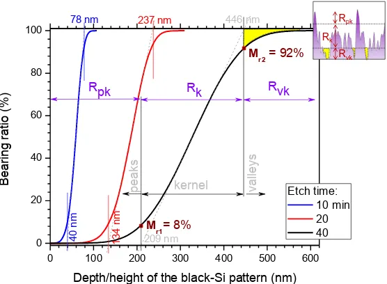
Figure A2.Bearing ratios of AFM traces (Fig.1(b,c)) of b-Si etched for 10, 20 and 40 min. See text for
definitions of the parameters marked on the the Firestone–Abbott bearing curve (standards DIN4776; STN ISO 13 565-2). Inset illustrates schematically the peak, kernel, and valley extent on actual AFM profile of 40 min etched Black-Si; yellow area-mark corresponds to the air pockets in the b-Si pattern which have height (depth) extent ofRvk.
of TiO2. Even such a thin TiO2layer acts as an anti-reflection coating and creates higher light intensity
E2inside Si nano-pyramid. The anti-reflection property of TiO2would be even more pronounced in
water solutionn≈1.3 at visible wavelengths as compared with airn=1.
FigureA2shows the Firestone–Abbott (F-A) bearing curves of b-Si etched for different times. The F-A curve is the cumulative probability density function of the surface profile’s height which is calculated by integrating the profile of AFM trace. Each curve can be separated into the peak, kernel and valley sections after linear fit (tangential section) of the central part of the bearing ratio (see the marking for the 40 min etched sample). The positions of the minimum and maximum depth/height of the linear section of the AFM scan at intersections at bearing ratios of 0 and 100%, respectively, defines the kernel section (209 and 446 nm in Fig.A2). At those depth(height) values, the actual bearing ratios readsMr1=8% andMr2=92%, which are are the mass ratios (DIN4776 standard). The area below
the F-A curve up to the pointMr1represents the mass (an integral) of the most protruding peaks of
surface roughness (the peaks region). The mass ratio pointMr2defines the point, which is excludes
mass of the most deep valleys (the valleys region). The kernel roughness depthRkis the thickness of
the kernel at the flattest part of the bearing curve with the largest increase of material under the bearing curve. The reduced peak heightRpkand the reduced valley depthRvkcorresponds to the thickness
of the bearing curve above (below) the central kernel profile, respectively. These parameters can be defined for surfaces etched for different times (Fig.A2) and lay foundation for statistical analysis of different surfaces.
The depth (height) profile is self-similar when roughness is investigated at different scales, hence is self-affine [28]. The Weierstrass-Mandelbrot (W-M) function is used for characterization of the height profilez(x)along scan in x-direction. The W-M function has a fractal dimension,D[28]:
z(x) =G(D−1)
∞
∑
n=nl
cos(2πγnx)
γn(2−D)
; 1<D<2; γ>1, (A1)
whereGis a scaling constant,γn ≡1/λnis the frequency mode corresponding to the reciprocal of
roughness wavelengthλn; the low cut-off frequency is defined by the lengthL(AFM scan length here)
asγnl =1/L. The fractal dimensionD= logN
logm, wheremis the magnification andNis the number of
self-similar segments 1/m, which form a line of unity length under magnificationm((1/m)×m=1); a one-dimensional linear segment is considered here as an example).
The fractal dimensionDcan be found from the power spectrum ofz(x), which is superimposed of infinite number of frequency modes and defines the amplitude of the roughness profile at different scales (AFM profile is considered here) [28]:
S(ω) = G
2(D−1)
2 lnγ ·
1
ω(5−2D)
. (A2)
If the power spectrumS(ω)is known, it is possible to calculate statistical parameters of the surface: the variances of the height, the slope and the curvature at different frequencies.
Another practical method to define the fractal dimension is based on the auto-correlation of AFM image (trace) [29]:R(m,n)wherem,nare integers describing a shift in x and y-directions, respectively, of the original imagez(x,y)which is made inNdata acquisition steps. Then the structure function is defined asS(m,n) =2S2q(1−R(m,n)), whereSqis the root mean square roughness. Then the structure
function of a self-similar pattern along the chosen directionτfollowsS(τ) =Kτ2(2−D)law [29], where
Kis the pseudo-topothesy (defines the absolute amplitude of spatial frequencies) andDis the fractal dimension. Nanoscale self-similar surface roughness from 20 nm to 300 nm (min-max height) was demonstrated on a thermally rescalled polystyrene coated with gold [30]. By changing scale of SEM images, self-similarity and fractal nature of such surfaces was evidenced.
the image provides direct estimate of the fractal dimensionDfrom the slope when log-log plot is made N(r)vs.r. A systematic structure analysis by bearing ratio and fractal dimension of nanostructures is urgently required for understanding their link with biocidal (anti-viral and antibacterial) properties of such surfaces, e.g. b-Si [2].
References
1. Jansen, H.; de Boer, M.; Legtenberg, R.; Elwenspoek, M. The black silicon method: a universal method for determining the parameter setting of a fluorine-based reactive ion etcher in deep silicon trench etching with profile control.Journal of Micromechanics and Microengineering1995,5, 115. doi:10.1088/0960-1317/5/2/015. 2. Ivanova, E.P.; Hasan, J.; Webb, H.K.; Gervinskas, G.; Juodkazis, S.; Truong, V.K.; Wu, A.H.F.; Lamb, R.N.; Baulin, V.; Watson, G.S.; Watson, J.A.; Mainwaring, D.E.; Crawford, R.J. Bactericidal activity of nanostructured black silicon.Nature Commun.2013,4, 2838.
3. Pham, V.T.H.; Truong, V.K.; Mainwaring, D.; Guo, Y.; Baulin, V.; Kobaisi, M.A.; Gervinskas, G.; Juodkazis, S.; Zeng, W.R.; Doran, P.; Crawford, R.J.; Ivanova, E.P. Nanotopography as a trigger for the microscale, autogenous and passive lysis of erythrocytes. J. Mater. Chem. B2014,2, 2819 – 2826.
4. Langer, C.; Prommesberger, C.; Ławrowski, R.; Schreiner, R.; Serbun, P.; Müller, G.; Düsberg, F.; Hofmann, M.; Bachmann, M.; Pahlke, A. Field emission properties of p-type black silicon on pillar structures. J. Vacuum Sci. Technol. B2020,34, 02G107.
5. Seniutinas, G.; Gervinskas, G.; Verma, R.; Gupta, B.D.; Lapierre, F.; Stoddart, P.R.; Clark, F.; McArthur, S.L.; Juodkazis, S. Versatile SERS sensing based on black silicon. Optics Express2015,23, 6763 – 6772.
6. Šˇcajev, P.; Malinauskas, T.; Seniutinas, G.; Arnold, M.D.; Gentle, A.; Aharonovich, I.; Gervinskas, G.; Michaux, P.; Hartley, J.S.; Mayes, E.L.H.; Stoddart, P.R.; Juodkazis, S. Light-induced reflectivity transients in black-Si nanoneedles.Solar Energy Mater. Solar Cells2016,144, 221–227.
7. Nishijima, Y.; Komatsu, R.; Ota, S.; Seniutinas, G.; Balˇcytis, A.; Juodkazis, S. Anti-reflective surfaces: Cascading nano/microstructuring. Appl. Phys. Lett.: Photonics2016,1, 076104.
8. Shoji, T.; Mototsuji, A.; Balcytis, A.; Linklater, D.; Juodkazis, S.; Tsuboi, Y. Optical tweezing and binding at high irradiation powers on black-Si.Sci. Reports2017,7, 12298.
9. Pekarek, R.T.; Christensen, S.T.; Liu, J.; Neale, N.R. Energetic Effects of Hybrid Organic/Inorganic Interfacial Architecture on Nanoporous Black Silicon Photoelectrodes.Sustainable Energy and Fuels2019,
3, 1600–1667.
10. Yang, F.; Aguiar, J.A.; Fairchild, M.; Vakki, W.; Younan, S.; Zhou, Y.; Zhuo, L.; Gu, J. Dual Protection Layer Strategy to Increase Photoelectrode–Catalyst Interfacial Stability: A Case Study on Black Silicon Photoelectrodes. Adv. Mater. Interfaces2019, p. 1802085.
11. Oh, K.; Joanny, L.; Gouttefangeas, F.; Fabre, B.; Dorcet, V.; Lassalle-Kaiser, B.; Vacher, A.; Meriadec, C.; Ababou-Girard, S.; Loget, G. Black Silicon Photoanodes Entirely Prepared with Abundant Materials by Low-Cost Wet Methods. ACS Appl. Energy Mater.2019,2, 1006–1010.
12. Yu, Y.; Zhang, Z.; Yin, X.; Kvit, A.; Liao, Q.; Kang, Z.; Yan, X.; Zhang, Y.; Wang, X. Enhanced photoelectrochemical efficiency and stability using a conformal TiO2 film on a black silicon photoanode.
Nature Energy2017,2, 17045.
13. Yao, X.; Schneider, C.W.; Lippert, T.; Wokaun, A. Manipulation of ion energies in pulsed laser deposition to improve film growth.Appl. Phys. A2019,125, 344.
14. Gervinskas, G.; Seniutinas, G.; Hartley, J.S.; Kandasamy, S.; Stoddart, P.R.; Fahim, N.F.; Juodkazis, S. Surface-enhanced Raman scattering sensing on black silicon. Annalen der Physik2013,525, 907–914. 15. Balˇcytis, A.; Ryu, M.; Seniutinas, G.; Nishijima, Y.; Hikima, Y.; and, M.Z. Si-based infrared optical filters.
Opt. Eng.2015,54, 127103 – 127103.
16. Buividas, R.; Fahim, N.; Juodkazyt ˙e, J.; Juodkazis, S. Novel method to determine the actual surface area of a laser-nanotextured sensor. Appl. Phys. A2013,14, 169–175.
17. Juodkazis, K.; Juodkazyt ˙e, J.; Šebeka, B.; Savickaja, I.; Juodkazis, S. Photoelectrochemistry of silicon in HF solution. J. Solid State Electrochem.2013,17, 2269–2276.
18. Brack.; Dann, S.E.; Wijayantha, K.; Adcock, P.; Foster, S. An assessment of the viability of hydrogen generation from the reaction of silicon powder and sodium hydroxide solution for portable applications.
19. Mizeikis, V.; Kowalska, E.; Juodkazis, S. Resonant localization, enhancement, and polarization. In
Nanoplasmonics: Advanced Device Applications; J W M Chon.; Iniewski, K., Eds.; CRC Press, 2009; p. 126–134. 20. Si, W.; Pergolesi, D.; Haydous, F.; Fluri, A.; Wokaun, A.; Lippert, T. Investigating the behavior of various cocatalysts on LaTaON2 photoanode for visible light water splitting. Phys. Chem. Chem. Phys. 2017,
19, 656–662.
21. Yang, J.; Liu, H.; Martens, W.N.; Frost, R.L. Synthesis and Characterization of Cobalt Hydroxide, Cobalt Oxyhydroxide, and Cobalt Oxide Nanodiscs. J. Phys. Chem. C2010,114, 111–119.
22. Stevens, M.; Kast, M.; Trotochaud, L.; Smith, A.; Boettcher, S. Cobalt–Iron (Oxy)hydroxide Oxygen Evolution Electrocatalysts: The Role of Structure and Composition on Activity, Stability, and Mechanism.J. Am. Chem. Soc.2015,137, 10.1021/jacs.5b00281.
23. Zhang, M.; de Respinis, M.; Frei, H. Time-resolved observations of water oxidation intermediates on a cobalt oxide nanoparticle catalyst. Nature Chem2014,6, 362–367.
24. Juodkazis, K.; Juodkazyt ˙e, J.; Kalinauskas, P.; Jelmakas, E.; Juodkazis, S. Photoelectrolysis of Water: Solar Hydrogen - Achievements and Perspectives. Opt. Express: energy express2010,18, A147–A160.
25. Juodkazyt ˙e, J.; Seniutinas, G.; Šebeka, B.; Savickaja, I.; Malinauskas, T.; Badokas, K.; Juodkazis, K.; Juodkazis, S. Solar water splitting: efficiency discussion.Int. J. Hydrogen Energy2016,41, 11941 – 11948. 26. Wang, Y.; Ge, H.X.; Chen, Y.P.; Meng, X.Y.; Ghanbaja, J.; Horwat, D.; Pierson, J.F. Wurtzite CoO: a direct
band gap oxide suitable for a photovoltaic absorber. Chem. Commun.2018,54, 13949–13952.
27. Berenschot, E.; Jansen, H.V.; Tas, N.R. Fabrication of 3D fractal structures using nanoscale anisotropic etching of single crystalline silicon. J. Micromech. Microeng.2013,23, 055024.
28. Majumdar, A.; Bhushan, B. Role of Fractal Geometry in Roughness Characterization and Contact Mechanics of Surfaces. J. Tribol.1990,112, 205 – 216.
29. ¸S ¸Talu.; Bramowicz, M.; Kulesza, S.; Pignatelli, F.; Salerno, M. Surface Morphology Analysis of Composite Thin Films based on Titanium-Dioxide Nanoparticles.Acta Physica Polonica2017,131, 1529–1533. 30. Balcytis, A.; Ryu, M.; Seniutinas, G.; Stoddart, P.R.; Mamun, M.; Morikawa, J.; Juodkazis, S. Nano-rescaling
of gold films on polystyrene: thermal management for SERS.Nanoscale2017,9, 690–695.