1784
Multi-Band Rectangular Patch Antenna with F-Type
Defected Metal Structure
Rahul Kumar Garg1, Shobit Agarwal2, Raghuvir Tomar3
Department of Electronics & Communication, The LNM Institute of Information Technology, Jaipur1, 2, 3 Email: [email protected]1,[email protected]2, [email protected]
Abstract-In this work, a novel multi-band microstrip patch antenna having two “F” shape slits and one circular slot as defected metal structures are proposed. This antenna works on Four bands i.e. 2.38 GHz, 2.54 GHz, 4.98 GHz, and 5.56 GHz with sufficiently large bandwidth. This antenna provides return loss as high as 48 dB at one of the bands and more than 30 dB at other two bands and 18 dB at the remaining band. The antenna is designed on FR4 substrate with an area of 45*60 mm2 and yields bandwidth from 60 MHz to 210 MHz at different bands.
Index Terms-Microstrip Antenna, Return Loss, Impedance Bandwidth, Defected Metal Structures (DMS).
1. INTRODUCTION
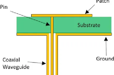
A microstrip antenna is generally a three-layered structure. It consists of a dielectric substrate having ground on one side while the patch is present on the other side of the substrate. Ground and patch are made up of conducting materials for e.g. copper. The main advantages of microstrip antennas over conventional antennas are compact size, moderately high gain and lower cross polarization. In the today’s world, people are interested in miniaturization of the devices and microstrip antennas come handy in that sense. A general microstrip antenna structure is shown in figure 1.
Figure 1: Microstrip Antenna with a coaxial feed
It is evident from figure 1, the outer conductor of the coaxial feed is connected to the ground and the inner conductor is connected to the patch via hole in the with feeding (coaxial, microstrip line, aperture coupled or proximity feed). The first step in designing a patch antenna is to choose an appropriate substrate which affects the electrical performance of the antenna. There is no ideal substrate but the choice of the substrate depends on the application. Available substrates are PTFE (Polytetrafluoroethylene), Polystyrene, Polyolefin, Alumina, Sapphire, Quartz, Rutile and Semiconductor Substrate etc. The dielectric constant range of the substrate for efficient operation of a patch antenna is (2.2 to 12).
1785 represents an equivalent resonant circuit and resonant
at different frequencies. This also provides an additional size reduction. Proper feeding and position of feed are used to match the impedance for excitation of the radiator which results in low return loss, high gain, bandwidth and directivity.
So, the position and width of the slit control the frequency band of the antenna. This technique provides the additional advantage of size reduction. By cutting a slot in the patch, the antenna is considered as two different resonators of different shape and size and makes an antenna dual or multiple bands operated for different mobile and wireless applications.
The equivalent circuit of the slit loaded patch is shown the following
Figure 2: Equivalent circuit of the slit loaded patch
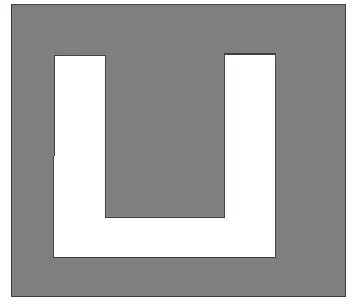
Figure3: Slot loaded patch
Fundamental bandwidth is defined as
And Fraction Bandwidth
( )
where fc= Center Frequency
The patch antenna behaves like a resonant cavity when it is excited using the coaxial feeding which generates strong field inside the cavity and a strong current flow on the surface of the patch and significant radiation starts using the fringing field effect.
In the presented work, two F-type slits and one circular defected metal structures are introduced in the patch. Defected metal structures allow us to reduce the size by increasing the effective length of the antenna and thus compact size antennas can be designed at lower frequencies. Defected Metal Structures (DMS) can be of any shape and size. Besides effective length, they also enhance bandwidth, gain and reduces cross polarization. These factors depend on size, shape, and location of the DMS.
2. CONVENTIONAL RECTANGULAR PATCH
ANTENNA:
To design a rectangular patch antenna, after selecting the substrate material, we have few design equations which provides the effective length, effective width, effective dielectric constant for the microstrip patch antenna.
A conventional rectangular patch antenna with patch dimensions 30mm X 40mm is designed over a 3.2 mm thick FR-4 dielectric substrate having 4.4 relative dielectric constant and loss tangent of 0.025. The substrate has an infinite ground plane and the overall size of the antenna is 50mm X 60mm. This antenna is fed through the 50 Ohm SMA connector.
1786 Figure 5: Return Loss Plot for the Rectangular Patch
Antenna.
Figure 4 represents the top view of the geometry of the proposed antenna in CST- Microwave studio software. Figure 5 shows the S11 vs Frequency graph for the antenna.
The result obtained shows that the antenna is multi-band antenna have a return loss of 32.45 dB at 3.36 GHz and corresponding bandwidth is 110MHz which is very low. Improvement in the performance of the rectangular patch antenna is further improved with the insertion of the some defected structure in the patch shape. Here the F-shape structure is used. Results obtained with the introduction of the F-Shape slits are presented in the next section.
3. PROPOSED RECTANGULAR PATCH
ANTENNA WITH F-TYPE SLITS:
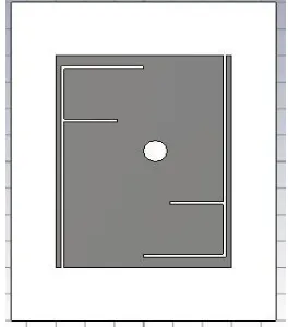
The geometry of the conventional rectangular patch antenna is modified to improve the performance. As shown in the following figure that the two F-Type slits are introduced in the geometry of the patch. The geometry of the inserted slits are the same, the only difference is the orientation of the insertion.
Figure 6: Design dimensions of the proposed antenna.
Figure. 7: Prototypes of the Defected Metal Structure As shown in figure 8, a rectangular patch is designed with two F-type slits and one circular slot in the patch. A prototype of the F-type slits is shown in figure 7 where L = 38 mm, L1 = 14 mm, L2 = 9 mm, L3 = 10 mm, L4 = 27 mm and w = 0.5 mm. whereas the radius for the circular slot is r = 2 mm.
Figure 8: Top view of the proposed antenna This proposed antenna is again designed on the same FR-4 dielectric substrate with same design parameters and simulate on the commercially available software CST- Microwave studio. The design parameters for the proposed antenna are summarized in table 1.
Table 1: Parameters of the proposed antenna
Parameter Value
Substrate FR4
1787 Substrate Thickness 3.2 mm
Patch Length 30 mm Patch Width 40 mm Feed Point Location (x, y) (8 mm, -6 mm) Ground Plane 50x60 mm2
The design equations used for the calculations are as follows:
The width of the patch
√
where the notations are in SI units and is the desired resonant frequency where c = 3x10⁸ m/Sec, the speed of light in vacuum.
Now, considering fringing field effects, the effective dielectric constant can be given by
[ ]
where h is the height of the substrate and W is the width of the patch calculated using Equation 1.
The increment in the length due to the fringing field can be calculated by the following equation
√
Length of the patch can be calculated by
√
( )
The proposed antenna is having four bands working in the range of 2.38 GHz – 5.56 GHz with reasonably good bandwidth and moderately high gain.
4. RESULTS AND DISCUSSION
All the simulations and designing of the proposed antenna is carried out on CST Microwave Studio software. Figure 9 shows the return loss S11 response
of the design. For impedance bandwidth, return loss higher than 10 dB is considered and with this
definition, this antenna is resonating on four bands given by 2.38 GHz, 2.545 GHz, 4.98 GHz, and 5.56 GHz with a bandwidth of 3-5%.
Figure 9: S11 response of the antenna
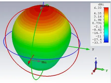
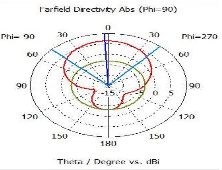
Figure 10: Far-field radiation pattern at 2.38 GHz
1788 Figure 12: Far-field radiation pattern at 2.54 GHz
Figure 13: Far-field radiation pattern at 2.54 GHz Figure 10-13 shows the far-field radiation pattern at 2.38 GHz and 2.54 GHz respectively. Polar representation of these graphs clearly indicates high directivity and gain as well. At 2.38 GHz, the half power beam width (HPBW) is 86.3 deg which results in directivity of 6.33 dB and at 2.54 GHz, HPBW = 88 deg which gives the directivity of 6.35 dB.
5. CONCLUSION
A novel multi-band rectangular patch antenna with defected metal structure is reported. The proposed antenna is working on four bands with sufficiently high bandwidth and providing good return loss. The directivity achieved is more than 6 dB and gain is also more than 5 dB.
6. ACKNOWLEDGEMENT
First of all, we would like to thank Prof. P. K. Singhal, Department of Electronics and Communication Engineering, MITS, Gwalior for supporting us in simulation and designing on their licensed CST version. We would also like to thank Prof. Raghuvir Tomar, Department of Electronics and Communication Engineering, The LNM Institute of Information Technology for his endless support and practical guidance that helped us to understand the roots of the analyzing and designing of the microstrip antenna.
REFERENCES
[1] R. Garg, P. Bhartia, I. J. Bahl and A. Ittipiboon “Microstrip antenna design handbook”, Artech House: New York, 2001
[2] Erik O. Hammerstad, “Equations For Microstrip Circuit Design”, Microwave Conference, Sept. 1975, 5th European.
[3] S. Dwivedi, “Effect of Thickness of Substrate on Antenna Design For Advance Communication”, Cloud Computing Data Science and Engineering-Confluence, Jan- 2017.
[4] S. Kumar, R. Tomar, “A Dual-Band Compact Printed Monopole Antenna Using Multiple Rectangle Shaped Defected Ground Structures and Cross Shaped Feed Line”, Microwave and Optical Technology Letters/ Vol. 57, No. 8, August 2015
[5] M. K. Idris, T. Imeci, “ Rectangular Shape Microstrip Patch Antenna With Multiple Slits and Slots”, 25th
Signal Processing and Communication Applications Conference (SIU), May 2017.
[6] G. Kumar, K. Ray “Broadband Microstrip Antennas”, Artech House Inc., 2003
[7] D. M. Pozar, “Microstrip Antennas”, Proc. IEEE, vol. 80, pp. 79-91, Jan. 1992.