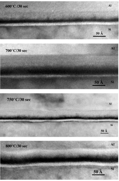
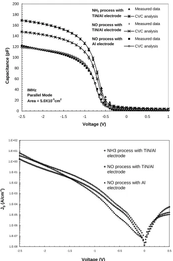
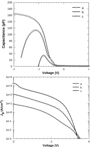
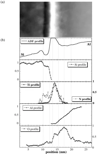
LI, WENMEI. Characterization of High-
κ
Gate Stacks in Metal-Oxide-SemiconductorCapacitors. (Under the direction of Dr. Dennis M. Maher)
The purpose of this research has been to use off-line characterization techniques to
establish material-specific properties of gate-stack constituents (i.e., high-κ dielectric stacks
and electrodes) and complete gate-stack structures. Hence, the characterization
methodologies were established to evaluate high-κ dielectrics at various processing levels,
which, in part, determine the final characteristics of an advanced gate-stack device. Material
systems that were investigated include: Al-O, Hf-Si-O, Zr-Si-O, Ti-O, Ta-O and Sr-Ti-O.
Various physical and electrical characterization techniques were used to establish
fundamental understandings of the materials selected, thin-film growth/deposition processes,
and gate-stack structures. General conclusions for stable and unstable gate-dielectric
materials have been established regarding the presence of a problematic interfacial layer at
the Si/dielectric interface, graded dielectric layers, and the stability of gate electrodes on
high-κ dielectrics.
The nanometer-scale chemistry of a gate-stack capacitor whose expected structure is
Si/SiOXNY/Ta2O5/TiN/Al was studied by high-resolution electron-energy-loss spectroscopy
in a scanning transmission electron microscope. Elemental profiles with near-atomic-level
resolution for Si, Ti, N, Al, and O demonstrate that the device structure deviates drastically
from the expectation and is chemically complex. It is concluded that the graded distribution
model that assumes abrupt interfaces and chemically discrete layers. This study impacted on
subsequent interpretations of flatband voltage extractions and electrical degradation
following backside metallization/postmetallization annealing for capacitors whose
dielectric-stack was based on Ta-O.
Detailed and extensive electrical characterizations of Pt/SiOx/Sr-Ti-O/SiMOS capacitors
were carried out to investigate reliability issues in a bi-layer gate dielectric. Based on these
studies, models are proposed to describe the carrier transport and dielectric degradation for a
Sr-Ti-O capacitor. It is concluded that conduction is dominated by Frenkel-Poole emission
from mid-gap trap levels. The trap barrier height is estimated to be 1.51eV. A model based
on the atomic and electronic structure of oxygen vacancies can account for the reported
leakage-current characteristics. In addition, it is tentatively proposed that anode-hole
injection and hole trapping control the dielectric degradation under gate injection.
CHARACTERIZATION OF HIGH-
κκ
GATE STACKS IN
METAL-OXIDE-SEMICONDUCTOR CAPACITORS
by
WENMEI LI
A dissertation submitted to the Graduate Faculty of North Carolina State University
in partial fulfillment of the requirements for the Degree of
Doctor of Philosophy
MATERIALS SCIENCE AND ENGINEERING
Raleigh
December 15, 2000
APPROVED BY:
Chair of Advisory Committee – D. M. Maher G. Lucovsky
J. J. Hren
To my parents, Li, Zhenfu and Ge, Ronghuai
and
iii
Wenmei Li was born to Zhenfu Li and Ronghuai Ge in Baotou, Inner-Mongolia, China.
Upon completion of high school at her hometown in 1984, she entered Xi’an Jiaotong
University, Xi’an, China, where she majored in Materials Science and Engineering. She
spent seven years there and received her Bachelor and Master degrees in 1988 and 1991,
respectively. Her research project for the Master’s degree focused on surface modification of
metallic materials by thin-film deposition (CVD, PVD, etc.). She then joined Yangzhou
University as an assistant professor in the College of Engineering, where she lectured
“Physical Metallurgy”, “Engineering Materials”, and “Professional English for Mechanical
Engineers”. The research projects she worked on were “plasma and laser co-assisted CVD
silicon nitride”, “properties and technologies of electroless-plated nickel-composite
coatings”.
Motivated to pursue a Ph. D. degree, she applied to graduate schools in the United State.
In the fall of 1997, she was awarded a research assistantship in Dr. Narayan’s group,
Materials Science and Engineering Department at North Carolina State University (NCSU).
The second semester, she worked for the department as a TA of an undergraduate course
“Electronic Properties Laboratory” and started taking courses in semiconductor physics and
fabrication, where she found what her interests really were. In May of 1998, she was awarded
a research assistantship by Dr. Dennis M. Maher in the SRC/SEMATECH Research Center
for Front End Processes, working on a gate-stack study for advanced MOS technology. Her
Upon finishing her Ph. D. in December of 2000, she will join the Advanced Micro
Devices, Inc., working in a non-volatile memory technology development group at
Sunnyvale, California.
v
I am deeply indebted to my teacher, Dr. Dennis M. Maher, for providing me an opportunity
to be his student, for leading me to this active research area, and making possible a life that
could not have been imagined just three years ago. Thanks for his support, guidance, wisdom
and kindness in teaching and encouraging me, not only professionally, but also personally,
during my graduate studies at NCSU. I also would like to acknowledge Dr. John J. Hren, Dr.
Gerald Lucovsky, and Dr. Veena Misra for the many useful technical discussions and the
educational courses they taught. Special thanks should go to my SRC mentors: Dr. Kurt
Eisenbeiser, Dr. David Muller, and Dr. Malcolm Bevan, for their help in many respects. I
would like to thank Dr. Jagdish Narayan for initially providing me with the opportunity for
graduate study at NCSU.
It has been a very pleasant experience to work in a large research center. I would like to
thank all the staff of NCSU’s microelectronics laboratory for their assistance during device
experiments. Many thanks to my former and current colleagues in Dr. Maher’s group,
including Meimei Xu, Shengqiang Wang, Dr. David Venables, Dr. Ranju Venables, Chadwin
D. Young, and Dr. Wei Liu. I also would like to extend my appreciation to individuals of
other groups in the SRC/SEMATECH Research Center for Front End Processes, including
Dr. Zhigang Wang, Dong Niu, Dr. Tonya Klein, Manoj Kulkarni, and Greg Heuss, for their
help and valuable discussions. I also like to thank Alex Kvit for his help in TEM.
Special thanks go to many of my friends who have cared about me for years. Their
Love to my parents, family, and sweet kisses to my daughter, the best gift from God. My
parents, Zhengfu Li and Ronghuai Ge, have always been with me in my life, and they
deserve my deepest gratitude. I want to thank my siblings for always being close to me.
Many thanks go to my in-laws for their love and unconditional support. Finally, my deepest
love and gratitude go to my husband, Guobin, for his love, patience, and enduring support.
Financial support for this research was provided by the SRC/SEMATECH Research
Center for Front End Processes at North Carolina State University. The Sr-Ti-O research was
conducted, in part, during a summer internship at Motorola Physical Sciences Research
Laboratories at Tempe, Arizona. I really appreciate the help from Jeffrey Finder, Dr. Kurt
Eisenbeiser, Dr. Alex Demkov, Dr. Peter Fejes, Dr. Ran Liu, and Dr. Shifeng Liu. Their
vii
Table of Contents
List of Tables ... ix
List of Figures ... x
1 Introduction... 1
1.1 A Bit of History ... 1
1.2 MOSFET Scaling – Approaches... 1
1.3 Challenges of Device Scaling in Front-end Processes... 2
1.3.1 Alternative Gate Dielectrics – Where are we going?...3
1.3.2 Gate Electrodes – Where are we going? ...5
1.3.3 Characterization of Material Systems...5
1.4 How to Meet These Challenges? ... 6
1.4.1 Selection Rules for Alternative Gate Dielectrics ...7
1.4.2 Proposed Gate-stack Structures ...9
1.4.3 Choosing an Engineered Interfacial Layer ...9
1.5 Interface Properties – Constraint Theory ... 10
1.6 Scope of the Present Research ... 12
1.7 Thesis Outline ... 14
2 Experimental and Characterization Methodologies... 19
2.1 MOS Device – Fabrication ... 19
2.2 Physical and Chemical Characterization Techniques ... 20
2.2.1 TEM, STEM, and EELS Analysis ...20
2.2.2 TEM Specimen Preparation Techniques – Wedge versus Conventional Dimpling...22
2.2.3 X-ray Photoelectron Spectroscopy ...23
2.2.4 Narrow Resonance Nuclear Reaction Profiling...23
2.3 Electrical Characterization Techniques ... 24
2.3.1 C-V Measurement...24
2.3.1.1 C-V Modeling and Simulations ... 24
2.3.1.2 C-V Data Acquisition and Analysis... 26
2.3.2 I-V Measurement ...28
2.3.3 Oxide Integrity Measurements...28
2.3.4 Interface State Characterization...29
2.3.4.1 Extraction of Dit from a Conductance Measurement ... 30
3 Characterizations of High-
κ
Gate Stacks ... 473.1 Thermodynamically Stable Systems... 47
3.1.1 The Al-O System ...47
3.1.2 The Hf-Si-O and Zr-Si-O Systems ...48
3.1.3 Discussion ...50
3.2 Thermodynamically Unstable Systems... 53
3.2.1 The Ti-O System...53
3.2.2 The Ta-O System ...55
3.2.2.1 Process Optimization and Thermal Stability ... 55
3.2.2.2 Electrical Characterizations ... 56
3.2.2.3 Nano-scale Chemistry Study... 58
3.2.2.4 Discussion ... 60
3.3 Summary ... 62
4 Studies of Ultrahigh-
κ
Gate Stacks – Epitaxial SrTiO3... 794.1 Carrier Transport Mechanism in STO ... 79
4.2 Characterization of Oxide Charges... 106
4.3 Reliability Issue – Dielectric Degradation Under Stress ... 108
4.3.1 TZDB Characteristics ...108
4.3.2 TDDB Characteristics...110
4.4 Discussion ... 111
4.5 Conclusions... 113
5 Summary and Future Work... 124
5.1 Concluding Remarks... 124
5.2 Future Work ... 127
Appendix A. Mass-thickness Contrast for Amorphous Materials ... 129
A.1 General Approach for Single Atomic Species ... 129
A.2 General Approach for Compounds ... 130
A.3 Elastic Cross-section... 131
A.4 Inelastic Cross-section ... 131
A.5 Contrast Calculations ... 132
A.6 Resolution Considerations ... 133
A.7 Imaging Conditions... 135
A.8 Conclusion ... 136
Appendix B. Calculation of Silicon Surface Potential as a Function of Gate Bias ... 140
B.1 General Equations... 140
B.2 Accumulation Region ... 141
B.3 Inversion Region... 141
B.4 Example ... 143
ix
List of Tables
Table 1.1 Scaling of MOSFET at device and circuit level ... 15
Table 1.2 Technology generations predicted by The International Technology
Roadmap for Semiconductors: 1999... 15
Table 1.3 Front End Process Difficult Challenges – Issues related to gate
stacks... 16
Table 1.4 Nav and Cav for various gate dielectrics based on constraint theory... 16
Table 2.1 Basic conduction mechanisms and their temperature and voltage
dependence characteristics, according to [45] ... 35
x
List of Figures
Figure 1.1 (a) device dimensions before scaling, and (b) device dimensions
after constant-field scaling by a factor αα. ...17
Figure 1.2 Conduction and valence band offsets for metal oxides and silicates,
based on J. Robertson’s data...17
Figure 1.3 Schematic illustration of proposed gate stack structures with and
without an engineered interfacial layer...18
Figure 1.4 Interface-defects-generation probability in gate-stack structures with
and without an engineered interface layer ...18
Figure 2.1 Schematic representations of the MOS capacitors fabricated for this study; (a) field-oxide isolated capacitor and (b) blanket gate dielectric with the gate electrode defined by a shadow mask or
lithography. ...37
Figure 2.2a System configuration: the system is calibrated so the spindle is perpendicular to the platen and provides a real-time measurement of the amount of material removed in 1µµm increments via a digital dial indicator. The platen rotation speed, the sense of the rotation and the
load are variables. ...38
Figure 2.3b System configuration: the wedge angle is adjustable in increments of 0.02° using the micrometers located at the base of the spindle. Only the specimen makes contact with the abrasive during the polishing, ensuring that the angle remains approximately constant throughout
the polishing process...38
Figure 2.4c The schematics depict the angle adjustment plates and the orientation of the pivot points used to define the angles. Points B and C are micrometers that are oriented 90° from a fixed pivot point A. The line AC is parallel to the edge of the specimen. This design allows for true pitch and roll adjustments. The micrometers are used to adjust the angle of the lower specimen mounting plate. Axial (front-to-back) adjustments are made using micrometer B. Radial
(left-to-right) adjustments are made using micrometer C. ...39
Figure 2.5d Optical micrographs comparing TEM specimens in transmitted light. The color gradient in (a) is due to a gradual increase in thickness. The light orange color at the edge of the crystal indicates a thickness of ~1 µm. Wedge polishing shows much larger area of electron transparency along the edge of the specimen compared to dimple
Figure 2.6e Two-types of wedge specimens are shown schematically: (a) a razor-blade style specimen, where the interface of interest is parallel to the edge of the specimen, a cover slip is used for surface protection; and (b) door-wedge style specimen, where a sandwich is made by gluing two wafer pieces of interest facing each other and the interface of
interest is perpendicular to the edge of the specimen. ...40
Figure 2.7f Illustration of site-specific sampling from device wafers. Photomicrograph shows the desired site to be sampled and the direction through which cross sectioning must be achieved. These devices are capacitors terminated by a field oxide. The features of interest are a field-oxide at the bird’s beak and the gate-stack dielectric/electrode. A razor-blade style specimen is made in this
case...40
Figure 2.8 Wedge polishing: illustration of site-specific data. Low-magnification image showing a portion of a fully fabricated capacitor including the bird’s beak (FOX) isolation (in a); a high-resolution image showing the stacked-gate dielectric (in b); and the scaling factor for metric extractions as well as the extracted metrics
(right). ...41
Figure 2.9 Wedge polishing: illustration of a long uniformly thinned region of a poly-gate capacitor – a low-magnification micrograph (BF) (in a) and a high-resolution field-of-view showing the advanced gate dielectric (N/O) and poly-silicon gate electrode (in b). The ion
milling time was ~ 10 minutes...41
Figure 2.10 Schematic illustration of the quantum mechanical effect in NMOS at the inversion region. The discrete energy levels are formed inside the potential well at the interface. The lowest subband energy level is above from the conduction band edge. As a result of subband formation, the peak of the carrier concentration in QM case is shifted away from the interface as compared to the classical case, leading to a decreased capacitive contribution from the substrate, and hence, a capacitance equivalent oxide thickness higher than the physical
thickness...42
Figure 2.11 NCSU CVC simulations showing theoretical C-V plots in the ideal case as well as with quantum and/or poly-depletion effects. The NMOS capacitor parameters used for simulations are: tox = 2 nm,
VFB = -1.03 V, Nsub = 2 ×× 1017 cm-3, Npoly = 1 ×× 1020 cm-3, Area = 1 ××
10-4 cm2. The QM effect contributes 2.5 Å to CET. CET increases 3 Å when both quantum and poly-depletion effects are present at the
Figure 2.12 Equivalent circuits for a capacitance – voltage measurement; (a) 3-element model, (b) parallel equivalent circuit, and (c) series
equivalent circuit for MOS capacitor...44
Figure 2.13 Data refinement (correction) for C-V and G-V measurements; Refined (corrected) and measured capacitance and conductance at 1 MHz on capacitors with area = 5.24 ×× 10-4
cm2, rs = 200 ΩΩ. ...44
Figure 2.14 Equivalent circuits for conductance measurements; (a) MOS capacitor with interface trap time constant ττit = RitCit, (b) simplified
circuit of (a), (c) simplified circuit of (b), (d) measured circuit. ...45
Figure 2.15 Equivalent circuits for conductance measurements with tunneling oxide; (a) MOS capacitor with interface trap and DC leakage Gdc, (b)
simplified circuit of (a), and (c) measured circuit. ...45
Figure 2.16 Measured and refined (corrected) GP/ωω versus frequency at Vg = -1.1
V for a capacitor with high series resistance. ...46
Figure 2.17 Interface traps determined by conductance method; (a) corrected GP/ωω versus frequency at different gate bias, (b) interface trap level
density and interface trap time constant as a function of silicon
bandgap energy with respect to the valence band edge. ...46
Figure 3.1 Deposition condition, and expected versus realized structures of an Al-O thin film. HRTEM indicates that the film thickness is approximately 18 nm. Two distinct amorphous layers are observed with approximately equal thickness. The second layer has higher
atomic number/density compared to the first layer. ...64
Figure 3.2 (a) Narrow resonance nuclear reaction profile (NRP) of a thick 18 nm Al2O3 on Si. Model of results (shown in inset) shows two layers
with the top layer having an Al concentration corresponding to Al2O3. Auger depth profile of the same film (in c) showing the
appearance of Si at approximately 10 nm. (b) NRP data for a thin 3.5 nm Al2O3 film and (d) XPS spectrum from the same film showing
evidence for Al-O-Si silicate bonding. ...65
Figure 3.3 (a) Process flow of forming a gate stack with Hf-Si-O gate dielectric, and (b) the realized triple layer amorphous gate dielectric with Al electrode. (c) XPS spectrum of as deposit film with various sputtering time shows the silicate bonding state. (d) A double layer
amorphous gate dielectric with Pt gate electrode. ...66
an problematic interfacial layer between the Si substrate and high-κκ
layer. ...67
Figure 3.5 HRTEM images of Hf-O sample show the discontinuity of the problematic interfacial layer. Part of the field-of-view there is no obvious interfacial layer. Si lattice fringes terminate at the nominal
high-κκ layer...68
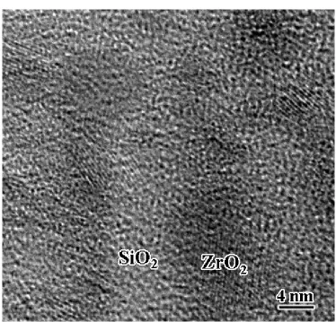
Figure 3.6 Phase-separation and crystallization for an RPCVD 10% ZrO2-SiO2
films after 900°°C, 30 seconds RTA in Ar...69
Figure 3.7 Process flow and physical structure of a Si/SiOxNy/TiO2/Al gate
stacks. The interfacial layer is of high quality. TiO2 layer is graded
and the interface with Al electrode is not smooth. ...70
Figure 3.8 HRTEM image shows the presence of crystallized region in the Ti-O
film and the crystallization seems start at the TiO2/SiOxNy interface. ...70
Figure 3.9 Al and Pt electrodes on TiO2 gate dielectrics with JVD nitride
interfacial layers. TEM images indicate a well-defined Al/TiO2
interface vs. a diffused Pt/TiO2 interface. C-V data show the
stretch-out caused by e-beam Pt deposition process (C-V raw data from Dr.
Ma’s group)...71
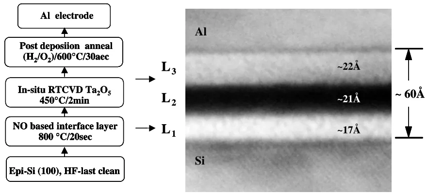
Figure 3.10 Process flow chart and HRTEM analysis for a Si/SiOxNy/Ta-O/Al
gate stack with NO interface process...71
Figure 3.11 Process flow chart and HRTEM analysis for a Si/SiOxNy
/Ta-O/TiN/Al gate stack with NO interface process. ...72
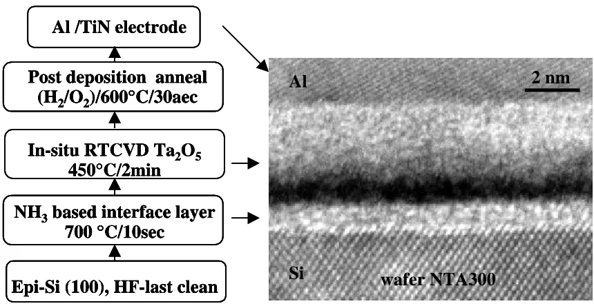
Figure 3.12 Process flow chart and HRTEM analysis for a Si/SiOxNy
/Ta-O/TiN/Al gate stack with NH3 interface process...72
Figure 3.13 TEM studies of thermal stability for optimized Ta-O gate stacks. ...73
Figure 3.14 Capacitance – voltage and current density – voltage characteristic of Ta-O gate stacks with different interface processes and gate
electrodes. ...74
Figure 3.15 Hysteresis measured at 1MHz after four cycles is 59 mV in flatband shift. The capacitor area is 5 ×× 10-5
cm2...75 Figure 3.16 Average values of the accumulation capacitance at -2.5 eV and the
current at –1.5 eV versus capacitor area and the linear least-squares
fit for Si/SiOxNy/TaxOy/TiN/Al capacitors. ...75
Figure 3.17 Comparison of measured C-V and I-V characteristics for capacitors
Figure 3.18 An ADF cross-sectional image of the gate-stack capacitor that was analyzed in this study is shown in (a). The Si (001) substrate is on the far left and the polycrystalline Al electrode is on the far right of the image. A normalized intensity profile from the ADF image and the normalized elemental profiles for Si, Ti, N, Al, and O are shown in (b). The six vertical lines are elemental-specific interfaces that bound five chemical-specific layers: (Si, Ti) OxNY , (Ta, Ti) OxNY ,
(Ti, Ta, Al) OxNY , (Al, Ti) OxNY , and Al2O3 plus metallic Al...77
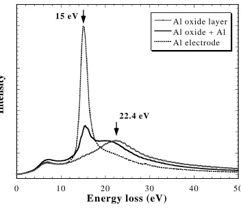
Figure 3.19 Typical deconvoluted low-loss spectra from polycrystalline Al and
the forth as well as the fifth chemical-specific layers ...78
Figure 4.1 Schematic illustration of various oxide charges and their possible
locations in bilayer gate stacks. ...115
Figure 4.2 STO interface state density and time constant as a function of silicon
bandgap energy with respect to the valence band edge. ...115
Figure 4.3 Results for bias temperature stress at 200°C for 10 min with (a) +5 V and then –5 V bias stress, and (b) –5 V and then +5 V bias stress. The measured data were corrected for series resistance effects using
Eq. (2.4). ...116
Figure 4.4 Jg – Vg measurement for STO capacitors, showing that there is no
abrupt increase in leakage current at high gate bias. ...117
Figure 4.5 Comparison of time-zero characteristics of STO and SiO2 gate stacks
in accumulation. The plots show Jg – Vg characteristics during and
after a time-zero measurement...117
Figure 4.6 Comparison of time-zero characteristics of STO and SiO2 gate stacks
at the inversion region. The plots show Jg – Vg characteristics during
and after time-zero measurements. ...118
Figure 4.7 Curve fitting result to the linear region of the time-zero I-V
characteristic for a SiO2 capacitor. ...118
Figure 4.8 Time-dependent characteristics of SiO2 gate stacks at –6 V gate bias
for different stressing times. ...119
Figure 4.9 (a) Gate current density – time and gate voltage – time characteristics of STO at 50 °°C. Gate injection was used for these measurements. (b) C-V and I-V characteristics before and after a
TDBD measurement. ...120
Figure 4.10 Time-dependent characteristics of STO capacitors with constant gate bias. Gate injection was used with various stress bias. The
Figure 4.11 Time-dependent characteristics of STO capacitors with constant gate bias at various temperature. Gate injection was used with –4 V stress bias. The measurements were done at elevated temperature to
accelerate the process...122
Figure 4.12 Schematic energy-band diagram showing Frenkel-Poole electron
emission and hole injection in an MOS structure under negative bias...123
Figure A.1 Mass thickness contrast obtained from oxide/nitride stack as a function of foil thickness, (a) effect of objective aperture size at a fixed accelerating voltage (200 KV), (b) effect of accelerating
voltage at a fixed objective aperture size (5 mrd)...137
Figure A.2 Demonstration of mass-thickness contrast from an O/N and an N/O stack by TEM micrographs. It is evident that the dual-layer structure can be differentiated and the contrast is reversed for O/N and N/O
stack as expected from theoretical calculation. ...138
Figure A.3 Resolution achievable with different objective aperture sizes for the 200 KV Topcon 002B with a UHR polepiece at NCSU (Cs = 0.4
mm)...139
Figure B.1 Si surface potential as a function of gate bias for a capacitor with STO gate dielectric. The capacitor parameters are: CET = 2.0 nm,
NA = 2.4 ×× 1015 cm-3, capacitor area = 5.24 ×× 104cm2, VFB = -1.28 V...144
Figure B.2 Electric field in oxide as a function of gate bias for a MOS capacitor
1
1 Introduction
1.1 A Bit of History
Since the invention of the first three-terminal device (i.e., the bipolar junction transistor) by
John Bardeen and Walter Brittain in 1948, the solid-state electronic industry has experienced
rapid growth over four decades [1]. Metal-Oxide-Semiconductor Field-Effect-Transistor
(MOSFET) devices were first proposed in 1960 and attracted considerable attention due to
their simplicity [2, 3]. Soon after the perfection of the Si-SiO2 interface and the development
of integrated technologies, MOSFETs became the workhorse devices in the silicon-based
semiconductor industry [2, 3].
Historically, device scaling, quantified by Moore’s Law, has driven MOS
integrated-circuit technologies [4]. Decreases in device feature size have provided improved
functionality at a reduced cost. Device line features have decreased at the rate of about 70%
every three years for most of the industry’s history. Cost per function has simultaneously
decreased at an average rate of about 25-30%/year/function [5].
1.2 MOSFET Scaling – Approaches
One fundamental restriction to the scaling of MOS structures has been photolithography,
which defines the smallest feature size, i.e., the channel length (L) [5]. For devices of channel
length comparable to the depletion regions around the source and drain, short-channel effects
associated with charge-sharing and punchthrough are intolerable. Thus, to make L small, the
depletion region widths have to be reduced by a heavily doped substrate and a lower supply
voltage. At the same time, silicon oxide thickness needs to be reduced to balance the
There are different sets of rules aimed at reducing the device size while keeping device
function [6-11]. One is constant-field scaling (CFS), according to which the resulting device
along with its depletion region is a scaled version of a larger device [6]. In Fig. 1.1, a MOS
transistor obtained by scaling all geometrical dimensions by the same factor, α, is illustrated.
The idea behind this scaling is to keep the electric field unchanged in a short-channel device
in order to maintain comparable characteristics and reliability relative to a long channel
device. However, the requirement of scaling the voltage by the same factor in CFS is difficult
to meet since the threshold voltage, VT, and sub-threshold slope, S, are not easily scaleable
[12]. If VT scales slower than other factors, drive current is reduced. Thus, a voltage higher
than desired has to be used, leading to constant voltage scaling (CVS), where the voltages
remain unchanged while device dimensions are scaled as CFS. However, CVS will result in
an extremely high electric field, which causes unacceptable leakage current, power
consumption, and dielectric breakdown as well as hot-carrier effects [8, 9]. To avoid the
extreme cases of CFS and CVS, a generalized scaling approach has been proposed where the
electric field is scaled by a factor of κ while the device dimensions are scaled by a factor of α
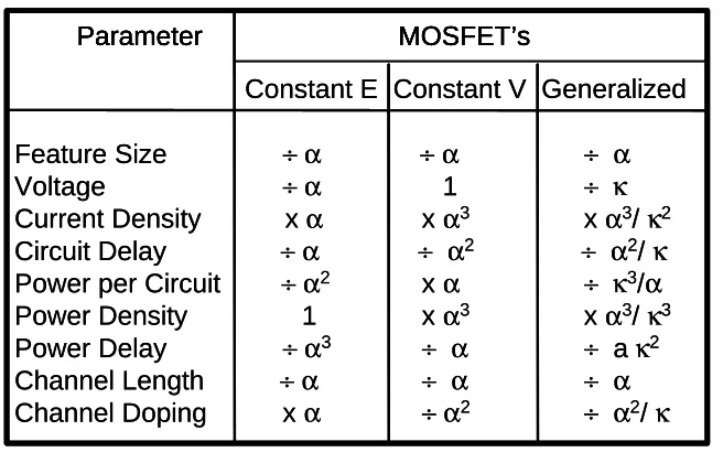
[7]. In Table 1.1, the scaling parameters for CFS, CVS and generalized scaling schemes are
tabulated.
1.3 Challenges of Device Scaling in Front-end Processes
Since 1992, the Semiconductor Industry Association (SIA) has coordinated the efforts of
producing what was originally the National Technology Roadmap for Semiconductors
(NTRS) and now the International Technology Roadmap for Semiconductors (ITRS), which
provides a 15-year outlook on the major trends of the semiconductor industry [5]. The future
number and the difficulties of the technical challenges continue to increase as the device
dimensions shrink, as is partially shown in Table 1.3. Traditional scaling, which has been at
the basis of the semiconductor industry for the last 30 years, is indeed approaching the
fundamental limits of the materials constituting the building blocks of the planar CMOS
process [5, 13-15]. Therefore, new materials have to be introduced into the basic CMOS
structure to replace and/or augment the existing ones to further extend device scaling.
1.3.1 Alternative Gate Dielectrics – Where are we going?
Among all the materials for MOS devices, the gate oxide remains one of the most critical,
since it plays a fundamental role in the concept of “field effect” control. Thermally grown
oxide (SiO2) has been used as a gate dielectric since MOSFET devices were first introduced
due to its process simplicity, nearly perfect insulator properties, and compatibility with the
silicon substrate. However, the phase-out of SiO2 is needed as early as the 100nm node
(circa 2005) due to a number of issues including high leakage currents and inadequate
reliability for a SiO2 dielectric layer less than 1.5 nm thick [5]. It has been well documented
that it will be difficult, if not impossible, to use SiO2 in this thickness regime [15, 16].
Extensive research is under way to meet the challenge of moving beyond the SiO2 era, i.e., to
replace the traditional silicon dioxide /dual-doped polysilicon gate stack process with high-κ
gate dielectrics and new gate electrode materials [17-32].
The capacitance, C, of a MOS capacitor is given as
eq
ox o SiO ox
o
t A t
A
c κε κ ε
2 =
where κ is gate oxide dielectric constant, εo the permittivity of vacuum, A the capacitor area,
and tox gate oxide physical thickness. By assuming the same capacitance is achieved using
SiO2 as the dielectric, the equivalent oxide thickness, toxeq, is given by
κ κSiO2 ox eq ox t
t = (1.2)
which means a thicker gate oxide of high permittivity (which will keep the leakage current
low) can hold the same gate capacitance as a thinner SiO2 dielectric. The near-term gate
dielectric solution has been chosen as ultra-thin silicon dioxide with a nitrided interface or
oxynitrided films based on years of research and a thorough understanding of their materials
characteristics [32-36]. A dielectric constant greater than 10 is suggested for intermediate
term and κ > 20 for the long-term solution. Much attention is being paid to the so-called
alternative high-κ gate dielectric materials such as Al2O3, Ta2O5, TiO2, HfO2, ZrO2, HfSiO4,
ZrSiO4, Y2O3, (Ba, Sr)TiO3 (BST), and SrTiO3 (STO). Unfortunately, a myriad of problems
are associated with these materials, including thermal instability on silicon, instability with
gate-electrode materials, small bandgap, undesired band alignment, large leakage current,
low channel mobility, and lower than expected dielectric constants of the as-deposited films
[37-41]. No suitable alternative high-dielectric-constant material and interfacial layer have
been identified with the stability and interface characteristics comparable to SiO2. It should
be mentioned that although oxynitride, SiOxNy, and silicon nitride, Si3N4, have higher
dielectric constants than SiO2, traditionally they are not grouped among alternative
1.3.2 Gate Electrodes – Where are we going?
Along with the replacement of SiO2, the replacement of dual-doped polysilicon is desired due
to limited active doping density and the polysilicon depletion effect which will cause the loss
of drive voltage in polysilicon [42, 43]. Dopant activation and penetration may also be major
problems with high-κ dielectrics, which generally require a low thermal budget to avoid
phase separation in dielectrics and/or reaction with the silicon substrate. For CMOS
technology, dual metals are required as replacements to achieve low threshold voltages, i.e.,
high work function (Fermi level near the silicon valence band edge) for PMOS and low work
function (Fermi level near the silicon conduction band edge) for NMOS. Chemical stability is
also a problem since many elemental metals form silicides if the dielectric has a SiO2
component [40]. Any reaction or intermixing at the electrode/dielectric interface will make
the issue very complicated due to the un-predictable modification of the work function and
resistivity. For compatibility with CMOS technology, the preferred solution to the integration
of two gate electrode metals is the use of a metal and compound of the same metal, such as
W and WN, so that a simple reaction might locally convert the metal into its compound [5].
The research that addresses the gate-electrode concerns has to be coupled with the alternative
gate dielectric. Therefore, the gate electrode research area has not been as active as that for
alternative gate dielectrics. Nevertheless, this research issue is starting to draw the attention
of the front-end processing society.
1.3.3 Characterization of Material Systems
As the push to find alternative dielectrics has grown in strength, a number of new concerns
dealing with physical, electrical and chemical characterizations of alternative gate
techniques, including capacitance-voltage (C-V) and current-voltage (I-V), are performed on
MOS capacitors and transistors to obtain parameters such as flatband voltage (VFB), threshold
voltage (VT), mobility (µ), substhreshold slope (s), average interface trap density (Dit), as
well as reliability parameters such as charge-to-breakdown (QBD), and time-to-breakdown
(tBD) [44, 45]. These parameters are directly impacted by the dielectric and gate electrode,
and are therefore used to evaluate the quality of the gate stack. Since SiO2 and polysilicon
have been used for nearly forty years, these characterization techniques have been refined to
a point that the extraction of parameters from MOS devices with SiO2 dielectric/poly-Si
electrodes is extremely accurate [46-48]. This is not the case, however, with the alternative
dielectrics that are being evaluated today [49]. Not only do the materials themselves make
electrical characterization difficult, but the use of stacked dielectric structures also adds to the
complexity of the problem. Thus, along with the search for an alternative dielectric comes the
need for a re-evaluation of traditional electrical characterization techniques. Meanwhile, the
nano-scale dimensions of the stacked structure is a big challenge to the physical and chemical
characterizations of gate stacks, high-resolution analytical techniques will be essential to
understand the near-atomic-level chemistries of these new materials systems and device
structures.
1.4 How to Meet These Challenges?
As is discussed in Section 1.3, the first consideration will be materials selections for both
gate dielectrics and gate electrodes, and the selection criteria are discussed in the following
sections. The appropriate gate-stack structure must be based on the materials systems that
1.4.1 Selection Rules for Alternative Gate Dielectrics
MOSFETs, while simple, depend critically on a reliable silicon/silicon oxide interface and it
took many years of intense research to understand how to obtain this interface reliably with
very low trap states [50, 51]. MOSFETs fabricated with alternative dielectrics exhibit
low-mobility values as a result of the low-quality interfaces between the dielectrics and silicon
[52, 53]. Hence, one of the major problems with a material other than SiO2 is the probability
that a very-thin SiO2 layer will still be required at the channel and/or gate electrode interface to preserve interface-state characteristics and channel mobility [54]. This interfacial layer
would severely degrade any benefits that accrue from the use of a high-κ dielectric. Even the
presence of only a single molecular layer of Si-O bonding to bridge between the silicon
substrate and a high-κ material is expected to present a physical limit to the scaling of
effective dielectric thickness below 0.3 nm [54].
To fully achieve the advantage of high-κ dielectrics, it is preferred that it sits directly on
silicon without any buffer layer. As a result, the possible reaction, mixing, or interlayer
formation between a dielectric and silicon during deposition or subsequent processing at
elevated temperatures has to be addressed. The initial consideration is the thermodynamic
stability of oxides in direct contact with silicon, where the thermodynamic calculations for
possible reactions between oxide and silicon need to be carried out. In the most
comprehensive study for the model system of a single component oxide in contact with
silicon at 1000K, Hubbard and Schlom evaluated the free energies of reactions for producing
known oxide or silicide products. Metal oxides were characterized as thermodynamically
stable or unstable in contact with silicon [40]. All binary oxides are thermodynamically
earth oxides (BeO, MgO, CaO, and SrO), the column IIIB oxide (Sc2O3, Y2O3, and La2O3), ThO2, UO2, ZrO2, HfO2, and Al2O3. Among these materials, BeO, MgO, CaO, SrO, Y2O3, Pr2O3, Nd2O3, ThO2, ZrO2, and Al2O3 have been studied and appear to be free of reaction layers on silicon. There are sufficient data to conclude that BeO, MgO, and ZrO2 are stable, but insufficient data for the others. It is also possible to have ternary or higher
multi-component oxides for direct integration with silicon, i.e., combinations of binary oxides that
are all thermodynamically compatible with silicon, e.g. ZrSiO4, LaAlO3, Y2O3-ZrO2,
MgAl2O4, etc. However, for those high-κ dielectrics that are unstable in direct contact with
silicon, an engineered interfacial layer will be required in order to take advantage of their
potential dielectric characteristics.
When it comes to the control of leakage current, which is crucial to MOS devices, the
band gap of the dielectric and band alignment at electrode/dielectric and dielectric/silicon
interfaces have to be considered as high barrier height favors low leakage current. Bandgaps
of 4-5 eV with a barrier height of > 1 eV is necessary to limit thermionic emission and
Fowler-Nordheim tunneling [5, 45]. Furthermore, negligible trap densities in dielectric layers
are required to suppress Frenkle-Poole tunneling [55, 56]. As a rule-of-thumb, for a high-κ
dielectric, the bandgap is usually small and hence has lower barrier height, which means a
leaky gate stack. In John Robertson’s work, he treated oxides as wide-band-gap
semiconductors and calculated their band alignments with silicon, as shown in Fig. 1.2 [39,
57]. Those high-κ dielectrics such as Ta2O5 have much lower gaps than silicon dioxide and
could have a different class of leakage problems due to Schottky emission of carriers into
band states. Furthermore, the band offsets for most transition metal oxides are quite
an engineered interfacial layer with high barrier height would be a feasible solution for those
high-κ/low-barrier-height dielectrics. According to Fig. 1.2, ZrO2, HfO2, Al2O3, Y2O3 have
suitable barrier height, however, these materials are fast ionic conductors with significant
oxygen ion diffusivity. From a band-alignment point of view, ZrSiO4 and HfSiO4 also would be promising choices, but their κ values are not very high.
Along with the high permittivity, chemical stability, and suitable band alignment, the
alternative gate dielectrics need to serve as an excellent diffusion barrier as well to prevent
gate electrode material or gate electrode dopant contamination of the transistor channel.
1.4.2 Proposed Gate-stack Structures
Based on the understanding of the chemical stability of the alternative gate dielectrics, as
well as the band alignment at the dielectric/silicon interface, the proposed gate stack
structures are shown in Fig. 1.3. For alternative gate dielectrics that are incompatible with
silicon and/or have inadequate barrier heights when they are in direct contact with silicon, an
engineered interfacial layer is mandated between the silicon substrate and the selected
alternative gate dielectrics. For so-called stable alternative gate dielectrics, no engineered
interfacial layer is required to fully achieve the potential of high permittivity.
1.4.3 Choosing an Engineered Interfacial Layer
As has been discussed so far, although the replacement of SiO2 with a single high-κ material
would be the ideal solution, it appears the transition from SiO2 to alternative dielectrics will
inevitably involve a stacked dielectric structure with an engineered interfacial layer. As to the
candidates for the interfacial layer, numerous studies have been conducted in this area [32,
silicon substrate and the alternative dielectric. Oxynitrides or nitrides have been the materials
of interest, since they have been used in industry for many years and the process step can be
easily integrated into the CMOS process flow. The deposition techniques involved are
furnace chemical vapor deposition (CVD), Jet vapor deposition (JVD) or remote plasma
enhanced CVD (RPCVD), and the growth can be controlled on the scale of an atomic layer,
which is crucial in achieving a thin equivalent oxide thickness (EOT). Recent results on this
topic indicate that nitride/silicon interface produces poor electrical interfaces due to interface
states and fixed charges [53]. However, a thin oxide interface (~ 0.6nm) is sufficient to
recover good electrical interface properties, which can be explained in terms of bonding
constraint theory (see Section 1.5) [33-35]. Also a monolayer of nitrogen at the
oxygen-silicon interface reduces tunneling current as shown in ref. [58]. Either an ultra-thin
oxynitride layer or an oxide layer with a nitrided interface would be the best choice for an
engineered interfacial layer [42]. An excellent summary on this topic can be found in ref.
[33].
1.5 Interface Properties – Constraint Theory
From an electrical characteristic point of view, the main concerns for an alternative gate
dielectric are the fixed charge and trap densities in bulk films and the silicon/dielectric
interfaces, which should be comparable to SiO2 and the Si/SiO2 interface, respectively [5]. Constraint theory can be used to evaluate qualitatively the interface properties. It was first
developed by Jim Phillips at Bell Labs to evaluate the formation of ideal glasses and
non-crystalline thin films with a random covalent network structure [37, 38, 54, 59]. It shows that
fully bonded, strain-free, three-dimensional, continuous-random networks can be formed at
with the applicable valence-force fields, Cav, and then matching constraint to the dimensionality of the network structure. Lucovsky and Philips extended the theory to
evaluate the interface qualities of gate-stack structures [37, 38, 54, 59]. Two metrics are used
to predict whether the differences between the bonding at the silicon/dielectric interfaces and
internal dielectric interfaces will result in increased densities of electrically active defects at
the interfaces, thereby limiting targeted levels of performance and reliability. The average
coordination of number of bonds per atom, Nav, is determined by the local network
coordination, and Cav (the average number of bond constrains per atom) is in turn determined by valence forces. The general relationship between the two parameters is given as Cav =
2.5Nav - 3. For the ideal network structure, Cav = 3, Nav* = 2.4. Interface defect creation at
the silicon/dielectric interface is proportional to (Nav-Nav*) 2
, where Nav* is the ideal average
coordination. Interface defect creation at an internal dielectric interface is proportional to
(∆Nav) 2
= (Nav - Nav)
2, where ∆N
av is the change in the average coordination of the number
of bonds at the internal dielectric interfaces.
In Table 1.4, the calculated values of Nav and Cav are tabulated for different gate
dielectrics. Interface defects creation probabilities, which are taken as (Nav-Nav*)2 and (∆Nav)
2
for gate stacks with and without engineered interface layers, respectively, are shown
in Fig. 1.4. Based on these results, defects at a silicon/dielectric interface and a
SiO2/dielectric internal interface follow the same trend, i.e., the higher the number of bonds
per atom for the dielectric, the worse the interface properties. As predicted by constraint
theory, Si3N4 has a rigid network structure and hence a higher number of bonds per atom.
or SiO2. Engineered interfacial layer candidates would be SiO2, oxynitride, (ZrO2)x(SiO2)1-x,
or Al2O3. Pseudo-binary alloys of high-κ oxide and SiO2 would improve interface properties
at the expense of lowering the dielectric constant. One thing that needs to be kept in mind is
that the above methodology is only useful for a general comparison among different
dielectrics. It can’t predict the defect type, defect energy level in the band gap, etc.
1.6 Scope of the Present Research
As discussed in previous sections, there are many critical issues related to the replacement of
SiO2. These issues must be systematically researched in order to further understand the viability of alternative gate dielectrics for future generations of devices. This thesis work has
focused on the study of high-κ gate stacks using physical and electrical characterization
techniques, to gain a better understanding of some important factors associated with
alternative gate dielectrics from both a theoretical and experimental points of view. Based on
the consideration of the main criteria for alternative gate dielectrics, i.e. thermal stability,
bandgap and band alignment as well as interface bonding properties, two kinds of gate-stack
structures, as proposed in Section1.4.2, were studied. One kind was an unstable material with
engineered interfacial layers, which included the Ti-O system with a JVD nitride interfacial
layer and the Ta-O system with an oxynitride interfacial layers that were produced by a NO
or NH3 processes. The second kind was stable materials deposited directly onto silicon,
which included the Al-O, Hf-Si-O and Zr-Si-O systems. For all the so-called stable material
systems, materials analyses indicate an uncontrollable interfacial layer formation at the initial
stage of deposition, which precludes the advantages of these materials; hence no further
detailed studies were performed on them. Many materials were only studied at the early stage
systems, namely Ta-O and Sr-Ti-O. Ta-O with different engineered interfacial layers was
chosen as an example of a system which is chemically unstable on silicon. As the only
perovskite material whose epitaxial growth on (001) Si has been realized to build functional
MOSFETs, single crystalline SrTiO3 is drawing much research attention as a potential gate
dielectric [23, 60-62]. Detailed electrical characterization study is performed on capacitors
with SrTiO3 as the gate dielectric. The material characterization focused on understanding
the physical and chemical properties of the gate stacks on an atomic or near-atomic scale.
The interfaces between dielectric/silicon, dielectric/electrode, internal interface between
stacked dielectrics, inter-diffusion and/or intermixing of layered structures, and thermal
stabilities of the gate stacks are the focus of the research.
With respect to electrical characterization, the first concern was to implement the
appropriate data extraction methods to eliminate effects from series resistance and/or gate
leakage. The conductance method was implemented to evaluate the interface states directly
from capacitors. Since the testing in the frequency domain couldn’t be realized at NC State at
the time this research was performed, the method was only applied to Sr-Ti-O work at
Motorola. The conduction mechanism, dielectric degradation mechanism and its reliability
were studied for Sr-Ti-O, given the gate stack structure is relatively simple so that the
assumption of abrupt interfaces and discrete band diagram for gate stacks are good
approximations. A capacitor was the main test structure due to its simplicity as well as
facilitating a fast learning and screening curve. Also, at the time this research was performed,
alternative dielectrics were not developed to the point where a sufficient number of
around the study of alternative gate dielectrics and interface characterization using both
theoretical and experimental approaches.
1.7 Thesis Outline
The experiments involved in and the characterization methods developed for this research are
presented in Chapter 2. Physical characterization is mainly concentrated on various
techniques that are available in transmission electron microscopes. For electrical
characterization, data refinement and a conductance method for Dit extraction are the focus.
The results for high-κ gate stacks with stable and unstable materials as gate dielectrics are
presented in Chapter 3. The highlight of this chapter is near-atomic-level chemistry for one
of the gate stacks studied, which demonstrates the complexity of the realized gate stack
structure as well as the necessity of establishing a fundamental understanding of the gate
stack chemistry.
The results from gate stacks with ultrahigh-κ single crystalline STO as gate dielectric are
presented in Chapter 4. As the only simple structure available for an in-depth electrical
characterization, studies addressing oxide charges, conduction mechanism, dielectric
breakdown and degradation behavior are included in this research.
The results and discussion that are concerned with the directions for future work are
given in Chapter 5. For a better understanding of gate-stack metrics and interface state
Table 1.1: Scaling of MOSFET at device and circuit level
Table 1.2: Technology generations predicted by The International Technology Roadmap for
Semiconductors: 1999
Year (Production) 1999 2002 2005 2008 2011 2014 Technology Node (nm) 180 130 100 70 50 35 MPU Gate Length (nm)140 85 65 45 32 22 Power Supply 2.5-1.8V 1.5-1.2V 1.5-1.2 V 1.2-0.9V 0.9-0.6V 0.6-0.5 EOT(nm) 1.9-2.5 1.5-1.9 1.0-1.5 0.8-1.2 0.6-0.8 0.5-0.6
EOT - equivalent silicon dioxide physical thickness
Constant E Constant V Generalized
Feature Size ÷ α ÷ α ÷ α
Voltage ÷ α 1 ÷ κ
Current Density x α x α3 x α3/ κ2
Circuit Delay ÷ α ÷ α2 ÷ α2/ κ
Power per Circuit ÷ α2 x α ÷ κ3/α
Power Density 1 x α3 x α3/ κ3
Power Delay ÷ α3 ÷ α ÷ a κ2
Channel Length ÷ α ÷ α ÷ α
Channel Doping x α ÷ α2 ÷ α2/ κ
Parameter MOSFET’s
α= Dimensional Scaling Factor; κ= Voltage Scaling Factor
Constant E Constant V Generalized
Feature Size ÷ α ÷ α ÷ α
Voltage ÷ α 1 ÷ κ
Current Density x α x α3 x α3/ κ2
Circuit Delay ÷ α ÷ α2 ÷ α2/ κ
Power per Circuit ÷ α2 x α ÷ κ3/α
Power Density 1 x α3 x α3/ κ3
Power Delay ÷ α3 ÷ α ÷ a κ2
Channel Length ÷ α ÷ α ÷ α
Channel Doping x α ÷ α2 ÷ α2/ κ
Parameter MOSFET’s
α= Dimensional Scaling Factor; κ= Voltage Scaling Factor
Parameter MOSFET’s
α= Dimensional Scaling Factor; κ= Voltage Scaling Factor
Parameter MOSFET’s
Table 1.3: Front End Process Difficult Challenges – Issues related to gate stacks
Table 1.4: Nav and Cav for various gate dielectrics based on constraint theory
Before 2005
Logic Gate Length > 65nm
2005 And After Logic Gate Length ≤≤ 65nm
Nitride Derivatives and High k Gate Stacks Ultra High k Gate Stack • Effective oxide thickness ≥≥1.2nm for
nitride derivatives, ≤≤ 1.2nm for high k • Achieve optimal channel mobility > 95%
of SiO2
• Minimize gate leakage mechanisms to achieve ≤≤ 1A/cm2
for high-performance logic and ≤≤0.001 A/cm2 for system LSI • Control boron penetration
• Minimize gate electrode depletion, e.g., polysilicon depletion
• Chemical compatibility of dual metal with appropriate work functions
• Effective oxide < 0.9nm • Chemical compatibility of dual
metal with appropriate work functions
• Acceptable channel mobility • Thermal budget and dielectric
stability
• CD (critical dimension) control • Gate leakage ≤≤ 1A/cm2
for high-performance logic and ≤≤ 0.001 A/cm2 for system LSI
• Cost-effective CMOS integration
Metrology Challenge
Optical, physical, electrical and chemical characterizations of gate dielectrics / electrodes
Dielectric Materials Nav Cav
SiO2 2.67 3
Ta2O5 2.86 4.14
Al2O3 3.0 4.5
Si3N4 3.43 5
TiO2 4 7
ZrSiO4 2.67 3
(a) (b)
Figure 1.1: (a) device dimensions before scaling, and (b) device dimensions after constant-field scaling by a factor α.
Figure 1.2: Conduction and valence band offsets for metal oxides and silicates, based on J.
Robertson’s data. E n e rg y ( e v ) - 6 - 4 - 2 0 2 4 6
Ta2O5
SiO2
Si3N4 BaTiO3
BaZrO3
ZrO2
HfO2 Al2O3
Y2O3ZrSiO4 1.1 Si 4.4 3.5 1.8 2.4 3.0 0.3 2.3 -0.1 3.4 0.8 3.3 1.4 3.4 1.5 4.9 2.8 3.6 1.3 3.4 1.5 E n e rg y ( e v ) - 6 - 4 - 2 0 2 4 6
Ta2O5
SiO2
Si3N4 BaTiO3
BaZrO3
ZrO2
HfO2 Al2O3
Figure 1.3: Schematic illustration of proposed gate stack structures with and without an
engineered interfacial layer
Figure 1.4: Interface-defects-generation probability in gate-stack structures with and without
an engineered interface layer
Si substrate
Gate electrode
Engineered interfacial layer Deposited alternative
gate dielectric internal dielectric
interface Si-dielectric
interface gate electrode -dielectric interface
Si substrate
Gate electrode
Deposited alternative gate dielectricSi substrate
Gate electrode
Engineered interfacial layer Deposited alternative
gate dielectric internal dielectric
interface Si-dielectric
interface gate electrode -dielectric interface
Si substrate
Gate electrode
Deposited alternative gate dielectric 0 10 20 30 40 502.6 2.8 3 3.2 3.4 3.6 3.8 4 4.2
S i/d ielectric interface
S iO2/dielectric interface
N av (N av -N av *)
2 value
(normalized to Si/SiO
2 interface value) Zr(Hf)SiO 4 Zr(Hf)O 2 T iO 2 Si
3N4
Al
2O3
T a
2O5
SiO
19
2 Experimental and Characterization Methodologies
2.1 MOS Device – Fabrication
The main test structures used in this research were MOS capacitors as shown schematically
in Fig. 2.1. Some capacitors were field-oxide isolated with active regions defined by
lithography. Other capacitors were fabricated using a process flow that included a
blanket-dielectric film and active areas defined by a shadow mask or lithography. Detailed device
fabrication processes can be found in references [50, 63, 64].
Various gate dielectrics were grown on Si (001) wafers. The thin-film growth techniques
were rapid-thermal chemical vapor deposition (TaxOy, HfSixOy, and ZrSixOy from Dr.
Kwong’s group at UT-Austin [17, 18]), plasma-enhanced chemical vapor deposition (AlxOy
from Dr. Parsons’ group at NCSU [20]), remote-plasma-enhanced chemical vapor deposition
(ZrSixOy from Dr. Lucovsky’s group at NCSU [65]), jet-vapor deposition (TiOx from Dr.
Ma’s group at Yale [25, 66]), reactive sputtering (HfSixOy from Dr. Misra’s group at NCSU
[67]), and molecular beam epitaxy (SrTiO3 from the Physical Sciences Research Laboratories
(PSRL) at Motorola Labs [24]). Some gate stacks had an engineered interfacial layer
deposited by jet-vapor deposition or chemical-vapor deposition. Detailed conditions for each
process can be found in the references given above. The principles involved in each growth
2.2 Physical and Chemical Characterization Techniques
To study the physical structures and the chemical characteristics of the gate stacks,
microstructural and microanalytical analyses were performed. High-resolution transmission
electron microscopy (TEM), electron-energy-loss spectroscopy (EELS) in a scanning
transmission electron microscope (STEM), X-ray photoelectron spectroscopy (XPS), and
narrow resonance nuclear reaction profiling (NRP) were the main techniques.
2.2.1 TEM, STEM, and EELS Analysis
Transmission electron microscopy is a very powerful materials and thin-film analysis
technique, which has the ability to provide structural and chemical information at very high
resolution (2 Å is now common). Many books have been written regarding its configuration
and theories of image contrast formation, which need not be repeated here [71-76]. The
conventional TEM is capable of imaging a specimen and returning selected-area-diffraction
patterns (SADP’s). High-resolution TEM (HRTEM) is a specialized TEM technique which
uses phase contrast to generate images which reflect the periodicity of the specimen and in
some cases can reveal atomic-level information. Interpretation of high-resolution images in
terms of atomic position is complex. The text by Spence is an excellent review of the theories
and practical applications of HRTEM [71]. For this research, HRTEM has been used to study
the dielectric/Si and dielectric/electrode interfaces. Most of the gate dielectrics are
amorphous films, and so-called mass-thickness contrast is the primary source to differentiate
dielectric layers in conventional TEM. The physics background for mass-thickness contrast
interpretation can be found in Reimer’s book [72]. Based on that theory, the contrast between
It is concluded from the results of those calculations that the conventional TEM can be used
to study the physical structures of gate stacks. However, it will be difficult to differentiate
amorphous layers of similar effective atomic number, Zeff, and density when the specimen is
thin. If high angle, incoherently scattered electrons are used to form the image, the contrast
will be enhanced. The intensity of these scattered electrons depends on Zeff only, thus
forming a so-called contrast image which contains elemental information with a
Z-dependence as high as Z2 [77]. With a very fine-probe size, images with atomic resolution can be achieved [13, 78], and they are called annular-dark-field images since the electron
beams are collected in a STEM using an annular-dark-field (ADF) detector.
Annular-dark-field images in STEM mode can be used to obtain first-order chemical information from
stacked-gate dielectrics. Detailed chemical and electronic studies of gate stacks at nanometer
or sub-nanometer scale can be achieved with electron-energy-loss spectroscopy. By
analyzing the energy distribution of electrons inelastically scattered with the specimen, the
local electronic structures can be inferred which in turn reveal details of the nature of these
atoms, their bonding and nearest-neighbor distributions, and their dielectric responses [72,
75, 76].
In this research, general analysis was done on a Topcon 002B ultra-high-resolution
transmission electron microscope with a high-resolution objective polepiece (Cs = 0.4 mm).
High performance analysis is achieved on a JEM-2010F filed-emission electron microscope
with an annular-dark-field detector as well as Gatan Imaging Filter (GIF) for EELS. The
probe size is ~ 0.2 nm in diameter. A study of the Ta-O system was completed using a
VG-HB501 STEM at the Cornell Center for Materials Research. The microscope was operated at
electron-energy-loss spectrometer. The incident electron-probe size was typically about 0.2
nm in diameter and the energy-loss spectra were recorded step-by-step at 0.2 to 0.3nm
intervals using a computer controlled scan generator [80], permitting analysis at 150 sites
across a typical structure. The ADF signal was recorded with a 10 mrad objective aperture
(for optimum probe size) and a 12.5mrad spectrometer entrance aperture. The ADF signal
and energy-loss spectra were acquired simultaneously. The spatial drift and high-voltage
stability were less than 0.05 nm/min and 0.2 eV/min, respectively. The energy resolution of
the spectrometer was 0.7 eV.
2.2.2 TEM Specimen Preparation Techniques – Wedge versus
Conventional Dimpling
A uniformly thinned TEM specimen with low contamination is crucial for microanalysis.
There are many ways to prepare specimens for the TEM, and some books are devoted to this
topic [81]. For cross-sectional TEM studies, two types of specimen preparation methods were
used: conventional dimple-polishing and the so-called “wedge-polishing” techniques. The
method of choice depends on both the type of material and the desired information. For the
wedge technique, a semiautomatic MultiPrepTM polishing system was used instead of a Tripod, where the physical layout of the MultiPrepTM polish tool enables precise alignment, accurate angle and pressure adjustment, and the alignment can be maintained during the
polishing process [82, 83]. It is possible to produce a wedge specimen with a long and
uniform sub-micron thickness at the tapered end. A wedge technique was used for
site-specific analyses and EELS where the specimen thickness and its uniformity are the primary
concerns. The tool layout, a comparison of the specimens made by dimple polishing and
A site-specific bird’s beak region of a capacitor and a long uniformly thinned region of a
poly-gate capacitor are shown in Fig. 2.3 and Fig. 2.4, respectively, demonstrating the
capability of the wedge technique.
2.2.3 X-ray Photoelectron Spectroscopy
X-ray photoelectron spectroscopy (XPS), also known as electron spectroscopy for chemical
analysis (ESCA), uses the interaction of X-ray photons with core-level electrons to identify
the chemical species at the sample surface. Electrons can be emitted from an orbital with
photoemission occurring for X-ray energies exceeding the binding energy. It is a surface
analysis technique and only sensitive to the upper 6 ~ 10 nm of the sample. The major
strength of XPS is that it allows chemical, not only elemental, identification. X-ray
photoelectron spectroscopy was used in this study to determine the elemental ratios in certain
films as well as their chemical states. More information about the technique can be found in
[84].
2.2.4 Narrow Resonance Nuclear Reaction Profiling
Narrow resonance nuclear reaction profiling (NRP) is a technique where a sample is
bombarded with an accelerated ion or proton beam of a particular energy so that a specific
nuclear reaction occurs. The nuclear reaction will lead to the emission of radiation at a
particular energy that is detected to determine the concentration of the atom of interest. The
maximum depth resolution is ~ 0.5nm. In this research, the depth distribution of 27Al concentration was obtained for thin AlxOy [20]. The narrow and isolated resonance in the
2.3 Electrical Characterization Techniques
A number of electrical measurements were performed to extract the electrical parameters
from various gate dielectrics. These measurements included capacitance-voltage (C-V),
current-voltage (I-V), and conductance in the frequency domain (G-f). From these
measurements, parameters such as equivalent oxide thickness (EOT), capacitance equivalent
oxide thickness (CET), interface trap density (Dit), oxide charge, and the current density at a
given bias voltage (J) were extracted. In this section, a brief review of the electrical
characterization techniques is given.
2.3.1 C-V Measurement
2.3.1.1 C-V Modeling and Simulations
Capacitance–voltage data provide a rapid means of determining important gate-stack and
dielectric parameters. The classical theory of C-V is well established [44, 85], but the
classical ideal theory must be modified for thin oxides because of substrate quantum
mechanical effects and polysilicon gate-electrode depletion effects [86]. Both of these effects
become more important factors in influencing the C-V characteristics for thin dielectrics (< 2
nm). Because of the sharp potential well for electrons (or holes) under strong inversion or
accumulation, the carriers are confined to a small spatial region and from quantum
mechanical considerations have localized energies above the traditional edge of the
conduction band. Additional semiconductor band bending is needed to achieve a given
surface-change density, and the carriers are located further from the surface than classically
predicted, as shown in Fig. 2.5. This phenomenon results in an apparent increase in the
the order of 0.25 to 0.3 nm. The polysilicon depletion effect arises because a finite
polysilicon doping density requires a finite depleted thickness of polysilicon to accommodate
the surface field, which again causes the electrically determined thickness to be larger than
the actual dielectric thickness. The polysilicon effect is asymmetrical with voltage, being
much larger when the polysilicon is depleted than when the polysilicon is under
accumulation. Reference [86] gives a thorough review of the topic, and related references can
be found there. Theoretical C-V plots predicted by NCSU’s CVC simulation in the classical
case as well as with quantum and/or poly-depletion effects are shown in Fig. 2.6. The QM
effect contributes 2.5 Å to CET, which increases ~ 3 Å when both quantum and
poly-depletion effects are present at the same time.
In order to use C-V measurements to extract oxide parameters, the effects discussed
above must be included in the conventional C-V modeling. Different modeling programs
have been developed and are used for simulation and/or oxide thickness extraction from
experimental data: NCSU's CVC [47], UC Berkeley's QMCV [87], UT Austin's UT QUANT
modeling programs [88], IBM's TQM [89, 90] (so-called one-point) to name a few.
Comparison studies on these models have been conducted and the preliminary results can be
found in [91]. North Carolina State University's CVC was used in this research since it has
been proved accurate, robust and very fast. The analysis program provides first-order models
for polysilicon depletion and quantum mechanical effects with a non-linear least-squares data
analysis approach [47]. With an accurate C-V theoretical model, C-V characteristics are
considered as a function of four variables:
(a) flatband voltage (or effective interface charge density);