Electronic Theses and Dissertations Theses, Dissertations, and Major Papers
2011
Hybrid MOS and Single-Electron Transistor Architectures towards
Hybrid MOS and Single-Electron Transistor Architectures towards
Arithmetic Applications
Arithmetic Applications
Guoqing Deng
University of Windsor
Follow this and additional works at: https://scholar.uwindsor.ca/etd
Recommended Citation Recommended Citation
Deng, Guoqing, "Hybrid MOS and Single-Electron Transistor Architectures towards Arithmetic Applications" (2011). Electronic Theses and Dissertations. 5390.
https://scholar.uwindsor.ca/etd/5390
This online database contains the full-text of PhD dissertations and Masters’ theses of University of Windsor students from 1954 forward. These documents are made available for personal study and research purposes only, in accordance with the Canadian Copyright Act and the Creative Commons license—CC BY-NC-ND (Attribution, Non-Commercial, No Derivative Works). Under this license, works must always be attributed to the copyright holder (original author), cannot be used for any commercial purposes, and may not be altered. Any other use would require the permission of the copyright holder. Students may inquire about withdrawing their dissertation and/or thesis from this database. For additional inquiries, please contact the repository administrator via email
Transistor Architectures towards
Arithmetic Applications
by
Guoqing Deng
A Dissertation
Submitted to the Faculty of Graduate Studies
through the Department of Electrical and Computer Engineering in Partial Fulfillment of the Requirements for
the Degree of Doctor of Philosophy at the University of Windsor
Windsor, Ontario, Canada
2011
Previous Publication
I. Co-Authorship Declaration
I hereby declare that this thesis incorporates materials that are the result of research
taken under the supervision of my supervisor Dr. C. Chen. Results related to this research
are reported in Chapters 3 through 6, inclusive.
I am aware of the University of Windsor Senate Policy on Authorship and I certify
that I have properly acknowledged the contribution of other researchers to my thesis, and
have obtained written permission from my co-author to include aforementioned materials
in my thesis.
I certify that, with the above qualification, this thesis, and the research to which it
refers, is the product of my own work.
II. Declaration of Previous Publication
This thesis includes seven original papers that have been previously published /
Thesis
Chapter Publication title / full citation
Publication status
Chapter 3
G. Deng and C. Chen, “Performance Analysis and
Improvement for Hybrid CMOS-SET Circuit Architectures,” in Proc. 1st Microsystems and Nanoelectronics Research Conf. (MNRC), Ottawa, Canada, 2008, pp. 109-112.
published
G. Deng and C. Chen, “Towards Robust Design of Hybrid
CMOS-SETs using Feedback Architectures,” in Proc. 10th IEEE-NANO, Seoul, Korea, 2010, pp. 1125-1129.
published
Chapter 4
G. Deng and C. Chen, “Full Adder Design using Hybrid
CMOS-SET Parallel Architectures,” in Proc. 9th IEEE-NANO, Genoa, Italy, 2009, pp. 206-209.
published
G. Deng and C. Chen, “Hybrid CMOS-SET Arithmetic
Circuit Design using Coulomb Blockade Oscillation Characteristic,” Journal of Computational and Theoretical Nanoscience (JCTN), vol. 8, no. 8, pp. 1520-1526, Aug. 2011.
published
Chapter 5
G. Deng and C. Chen, “Binary Multiplication using Hybrid
MOS and Multigate Single-Electron Transistors,” IEEE Transactions on Nanotechnology, July, 2011 (9 pages).
submitted
Chapter 6
G. Deng and C. Chen, “A Hybrid CMOS-SET Multiplier
using Frequency Modulation,” in Proc. 11th IEEE-NANO, Portland, Oregon, 2011, pp. 1167-1170.
published
G. Deng and C. Chen, “Frequency Synthesis for Arithmetic
Operations using SET/MOS Hybrid Architectures,” IEEE Transactions on VLSI Systems, August, 2011 (7 pages).
I certify that I have obtained a written permission from the copyright owner to include
the above published materials in my thesis. I certify that the above materials describe
work completed during my registration as graduate student at the University of Windsor.
I declare that, to the best of my knowledge, my thesis does not infringe upon anyone’s
copyright nor violate any proprietary rights and that any ideas, techniques, quotations, or
any other material from the work of other people included in my thesis, published or
otherwise, are fully acknowledged in accordance with the standard referencing practices.
Furthermore, to the extent that I have included copyrighted material that surpasses the
bounds of fair dealing within the meaning of the Canada Copyright Act, I certify that I
have obtained a written permission from the copyright owners to include such materials
in my thesis.
I declare that this is a true copy of my thesis, including any final revisions, as
approved by my thesis committee and the Graduate Studies office, and that this thesis has
Abstract
Metal-Oxide-Semiconductor Field-Effect Transistor (MOSFET) and Single-Electron
Transistor (SET) hybrid architectures, which combine the merits of both MOSFET and
SET, promise to be a practical implementation for nanometer-scale circuit design. In this
thesis, we design arithmetic circuits, including adders and multipliers, using SET/MOS
hybrid architectures with the goal of reducing circuit area and power dissipation and
improving circuit reliability.
Thanks to the Coulomb blockade oscillation characteristic of SET, the design of
SET/MOS hybrid adders becomes very simple, and requires only a few transistors by
using the proposed schemes of multiple-valued logic (MVL), phase modulation, and
frequency modulation. The phase and frequency modulation schemes are also further
utilized for the design of multipliers with more discussions.
Two types of SET/MOS hybrid multipliers are presented in this thesis. One is the
binary tree multiplier which adopts conventional tree structures with multi-input counters
(or compressors) implemented with the phase modulation scheme. Compared to
conventional CMOS tree multipliers, the area and power dissipation of the proposed
multiplier are reduced by half. The other is the frequency modulated multiplier following
This method involves the design of digital-to-frequency and frequency-to-digital
conversions which are also implemented with SET/MOS hybrid architectures. In this
context, we explore the implicit frequency properties of SET, including both frequency
gain and frequency mixing. The major merits of this type of multiplier include: a)
simplicity of circuit structure, and b) high immunity against background charges within
SET islands.
One of the biggest challenges associated with SET-based circuits is the background
charge effect. Background charges are mainly induced by defects or impurities located
within the oxide barriers, and cannot be entirely removed by today’s technology. Since
these random charges deteriorate the circuit reliability, we investigate different circuit
solutions, such as feedback structure and frequency modulation, in order to counteract
this problem. The feedback represents an error detection and correction mechanism
which offsets the background charge effect by applying an appropriate voltage through an
additional gate of SET. The frequency modulation, on the other hand, exploits the fact
that background charges only shift the phase of Coulomb blockade oscillation without
changing its amplitude and periodicity. Therefore, SET/MOS hybrid adders and
multipliers using the frequency modulation scheme exhibit the high immunity against
Acknowledgments
This research would not have completed without the support and encouragement from
my supervisor, peers, and family.
I would like to express my sincerest gratitude to my supervisor, Dr. C. Chen, who has
been providing me continuous support throughout my graduate studies. I am very grateful
to him for his academic guidance which inspires me and drives me to complete this
research work in time.
I would like to thank my committee members, Dr. S. Chowdhury and Dr. M.
Mirhassani from the Electrical and Computer Engineering, and Dr. S. Holger Eichhorn
from Chemistry and Biochemistry, for their valuable advice during my seminars and
constructive comments on this thesis.
A special thank to Dr. R. Rashidzadeh who has instructed me to conduct simulations
at the Research Centre for Integrated Microsystems (RCIM), and Dr. H. Wu who has
influenced me with his graduate teaching.
Finally, to my wife, my parents, and my parents-in-law, I am grateful for their support,
encouragement, and understanding. My wife, Jieqiong Gu, always believed in me and
Declaration of Co-Authorship / Previous Publication
...
iii
Abstract
...
vi
Dedication.
...
viii
Acknowledgments
...
ix
List of Figures
...
xiv
List of Tables
...
xviii
List of Abbreviations
...
xix
List of Symbols
...
xxi
1. Introduction ... 1
1.1 Motivations ... 1
1.2 Single-Electron-Tunneling Technology ... 2
1.3 Research Objectives ... 2
1.4 Thesis Organization ... 3
2. SET Background ... 6
2.1 Single-Electron Scaling ... 6
2.2 Orthodox Theory ... 8
2.3 SET Structure ... 9
2.4 Coulomb Blockade Oscillation ... 11
2.6 Background Charge Effect ... 17
2.7 Applications ... 18
2.8 Intrinsic Drawbacks ... 18
2.9 Fabrications ... 19
2.10Case Study: SIMON Simulations ... 22
3. SET/MOS Hybrid Architectures ... 29
3.1 Introduction ... 29
3.2 Hybrid MOS and SET Co-Simulation ... 30
3.3 Serial and Parallel SETMOS ... 31
3.3.1 Power Dissipation ... 35
3.3.2 Current Drivability ... 35
3.3.3 Temperature Effect ... 37
3.4 Robust Design against Background Charges ... 39
3.4.1 Adaptive Feedback Structure ... 39
3.4.2 Improved SET/MOS Hybrid ADC using Adaptive Feedback ... 43
3.5 Summary ... 50
4. SET/MOS Hybrid Binary Full Adders ... 51
4.1 Introduction ... 51
4.2 Implementations of SET/MOS Hybrid FAs ... 52
4.2.1 Multiple-Valued Logic (MVL) Scheme ... 52
4.2.2 Phase Modulation Scheme ... 57
4.2.3 Frequency Modulation Scheme ... 59
A. 1-bit FA ... 59
B. Multi-bit FA ... 61
4.3 Parameter Selection of the Proposed FAs ... 62
4.4 Summary ... 64
5. SET/MOS Hybrid Binary Tree Multiplier ... 65
5.2 Multi-Input Counters for Tree Multiplier ... 67
5.2.1 Phase Modulation Scheme ... 67
5.2.2 Primitive Implementation of (3:2) and (7:3) Counters ... 70
5.2.3 Enhanced Implementation of the (7:3) counter ... 74
A. Increased Temperature using Input Capacitor Array ... 74
B. Improved Reliability using Phase Adjustment Scheme ... 75
C. Increased Speed using Parallel SETMOS Structure ... 81
5.3 Implementation of Parallel Tree Multipliers... 83
5.3.1 Partial Product Generation (PPG) ... 83
5.3.2 Partial Product Accumulation (PPA) ... 84
5.3.3 Carry Propagation Addition (CPA) ... 85
5.4 Simulations and Discussions ... 87
5.4.1 Simulation of the Enhanced Type (7:3) Counter ... 87
5.4.2 Background Charge Effect ... 91
5.4.3 Area-Delay-Power Analysis ... 91
5.4.4 Comparisons ... 96
5.5 Summary ... 98
6. SET/MOS Hybrid Frequency Synthesis for Arithmetic ...
Applications ... 100
6.1 Introduction ... 100
6.2 SET Based Frequency Synthesis ... 102
6.2.1 Frequency Gain ... 102
6.2.2 Frequency Mixing ... 106
6.2.3 Sawtooth/Reverse-Sawtooth Wave Generation ... 109
6.2.4 SET/MOS Hybrid Frequency Synthesizer (FSR) ... 113
6.3 Frequency Modulated Arithmetic Operations ... 115
6.3.1 Digital-to-Frequency Converter (DFC) ... 115
6.3.2 Frequency-Modulated Arithmetic Circuits ... 118
6.3.3 Frequency-to-Digital Converter (FDC) ... 120
6.4.1 Background Charge Effect ... 127
6.4.2 Amplitude Effect of Input Sawtooth Wave ... 129
6.5 Summary ... 130
7. Conclusions and Future Work ... 131
7.1 Conclusions ... 131
7.2 Future Work ... 132
References ... 134
List of Figures
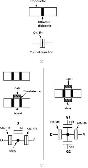
2.1: (a) Structure of a tunnel junction; (b) Structure of a single-electron transistor (SET)
where the left one is the one-gate SET and the right one is the two-gate SET.
(Reproduced with permission from [32]). ... 10
2.2: Electron tunneling mechanisms in the SET. (Reproduced with permission from [32]). ... 15
2.3: Constant current biased SET in SIMON simulator environment. ... 25
2.4: Effect of CLoad on VDS oscillation, where CLoad = 1aF, 10aF, 100aF, and 1fF. ... 25
2.5: Effect of IBias on VDS oscillation, where IBias = 2nA, 5nA, 8nA, and 11nA. ... 26
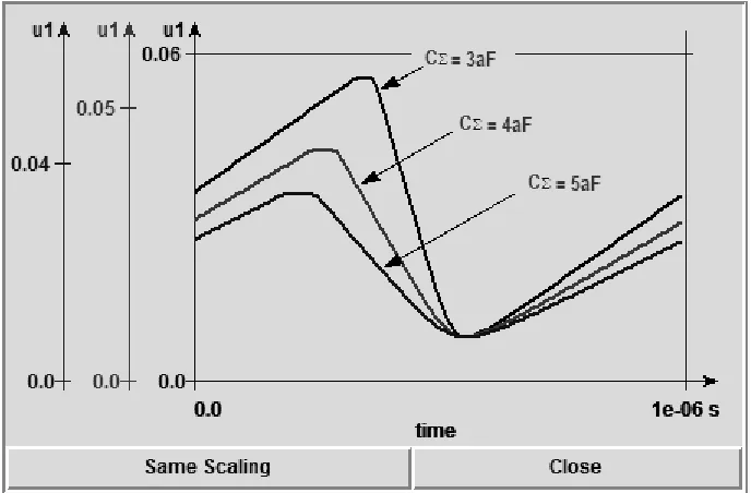
2.6: Effect of CΣ on VDS oscillation, where CΣ = 3aF, 4aF, and 5aF. ... 26
2.7: Effect of CG on VDS oscillation, where CG = 1aF, 2aF, and 3aF. ... 27
2.8: Effect of temperatureon VDS oscillation, where T = 1K, 11K, and 21K. ... 27
2.9: Effect of BCs on VDS oscillation, where BC = – 0.1e, 0, and 0.1e. ... 28
2.10: Effect of VGS2 on VDS oscillation, where VGS2 = –100mV, 0, and 100mV. ... 28
3.1: (a) Serial SETMOS; (b) Parallel SETMOS. ... 32
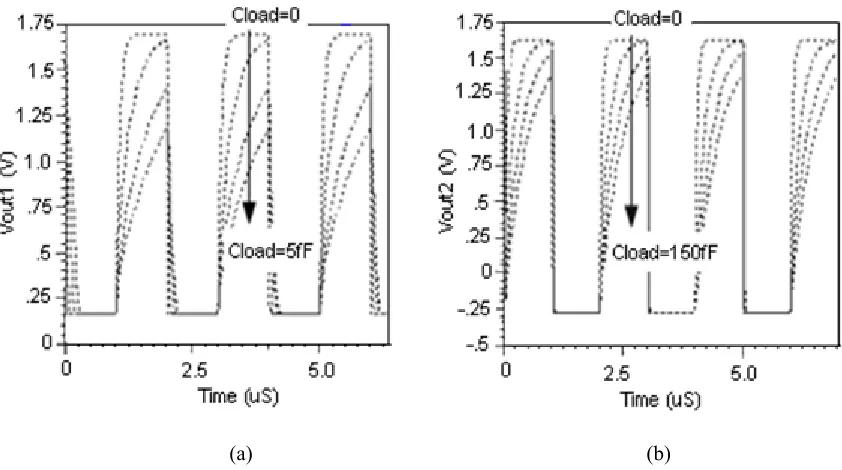
3.2: VDS|SET and output voltage oscillations where VOUT1 is the output of serial SETMOS and VOUT2 is the output of parallel SETMOS. ... 34
3.3: Transient analysis of serial and parallel SETMOSs where VIN, VDS|SET, VOUT1, and VOUT2 are defined in Figure 3.2. ... 36
3.5: Temperature effect on the output of serial SETMOS (a) and parallel SETMOS (b) ..
... 37
3.6: Parallel SETMOS with an adaptive feedback structure. ... 39
3.7: VDS|SET and VOUT oscillations of the parallel SETMOS (without feedback) with BCs
changing from –0.3e to 0.3e. ... 40
3.8: Simulation result of parallel SETMOS with adaptive feedback of Figure 3.6 where
BCs = 0, 0.1e, 0.2e, and 0.3e. ... 42
3.9: Parallel SETMOS with adaptive feedback used for the ADC units. ... 44
3.10: Simulation result of the circuit of Figure 3.9 with BCs = 0, 0.1e, 0.2e, and 0.3e.. . 45
3.11: (a) Input and output relationship of a 3-bit ADC circuit; (b) The feedback structure
with the biasing network used for the output bit D1; (c) The feedback structure with
the biasing network used for the output bit D0. ... 47
3.12: Improved 3-bit SET/MOS hybrid ADC with adaptive feedback structure. ... 48
3.13: Simulation results of the 3-bit SET/MOS hybrid ADC without (a) and with (b) the
feedback, where BCs = 0, 0.1e, 0.2e, and 0.3e. ... 49
4.1: (a) Parallel SETMOS with three SETs connected in parallel; (b) VDS|SET oscillation
and the voltage conversion of the NMOS transistor; (c) Output voltageoscillations used to realize carry and sum functions; (d) Overall schematic of 1-bit FA based on the MVL scheme. ... 56
4.2: (a) Overall schematic of a 1-bit FA based on the phase modulation scheme; (b)
VDS|SET oscillations used to realize sum and carry functions. ... 58
4.3: (a) Overall schematic of a 1-bit FA based on the frequency modulation scheme; (b)
VDS|SET oscillations with different digital inputs. ... 61
4.4: Overall schematic of a 2-bit FA based on the frequency modulation scheme. ... 62
4.5: Simulation result of a FA based on the MVL scheme using parameters in Table 4.2.
... 64
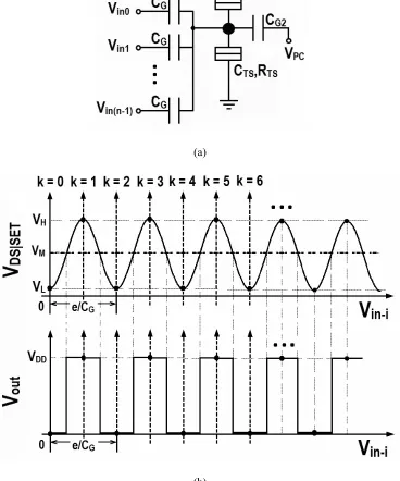
5.2: VDS|SET oscillations with the input gate capacitances of CG, CG/2, and CG/4 for SETs
used to realize dout0, dout1, and dout2, respectively. ... 72
5.3: Primitive type (3:2) (a) and (7:3) counters (b) based on the phase modulation scheme. ... 73
5.4: Implementation of a (7:3) counter with temperature enhancement using serial SETMOS and input capacitor array. ... 76
5.5: VDS|SET and output voltage oscillations used for reliability improvement. ... 78
5.6: Implementation of a (7:3) counter using phase adjustment scheme... 80
5.7: Parallel SETMOS followed by a CMOS inverter ... 82
5.8: VDS|SET oscillation with 33.3% duty cycle at the output for an AND gate that has increased reliability against BCs. ... 84
5.9: A 2-bit full adder implemented using a (7:3) counter. ... 86
5.10: Simulation result of the enhanced type phase modulated (7:3) counter. ... 90
5.11: Output of the (7:3) counter without phase adjustment scheme and no BC (a); without phase adjustment scheme and 0.1e BCs (b); with phase adjustment scheme and 0.1e BCs (c); and with phase adjustment scheme and 0.2e BCs (d). ... 93
6.1: (a) Constant current biased SET with two gate terminals; (b) The voltage oscillation of VDS vs. VGS at room temperature. ... 103
6.2: Time domain VDS oscillation for the SET of Figure 6.1 based on ramp VGS with slope of 1.6V/μs (a); sawtooth VGS with the amplitude and frequency of 1.6V and 1MHz (b); sawtooth VGS with the amplitude and frequency of 3.2V and 1MHz (c); and sawtooth VGS the same as the one in (b) but with CG = 0.2aF for SET (d). .... 105
6.4: (a) Current biased SET with a short-connection between the drain and the second
gate terminals (load capacitor exists but not shown here); (b) VDS oscillations
without (i.e., curve A) and with (i.e., curve B) the feedback, where dashed curves are shifted versions of curve A with VGS2 = 120mV, 180mV, 240mV, 300mV and
360mV (from right to left). ... 111
6.5: (a) Constant current biased SET with enhanced feedback strength; (b) VDS and VGS2
oscillations, where Gv increases from 1 to 8 with the step size of 1. ... 112
6.6: (a) Implementation of SET/MOS hybrid frequency synthesizer (FSR); (b) Symbol
of SET/MOS hybrid frequency synthesizer (FSR). ... 114
6.7: Block diagram of frequency modulated arithmetic operations. ... 115
6.8: (a) Implementation of a 3-bit digital-to-frequency converter (DFC); (b) Symbol of
3-bit digital-to-frequency converter (DFC). ... 116
6.9: Implementations of a 4-bit (a), 6-bit (b), and 8-bit (c) DFC. ... 117
6.10: Implementations of frequency multiplication (a), frequency division (b), and
frequency addition (c)... 119
6.11: One bit frequency comparator (a) and its symbol (b) as well as the frequency
comparisons under different input conditions (c) ... 121
6.12: Frequency comparator based one-bit FDC (a) and its symbol (b) as well as
frequency comparator based n-bit FDC (c). ... 123
6.13: Output voltage oscillations of 3-bit DFCs cascaded by three stages with the input
reference frequency being 1MHz and the digital operands of these stages configured as 3, 4, and 3. ... 125
6.14: Nonlinearity of the sawtooth wave at the output of DFC which has the same
frequency as the input. The bottom curve shows the difference between the real and ideal sawtooth outputs. ... 126
6.15:
List of Tables
3.1: Parameters of serial and parallel SETMOSs ... 34
3.2: Temperature effect on SET and MOSFET devices ... 38
4.1: Input and output relationship of a (3:2) counter ... 54
4.2: SET’s input-gate capacitance and the biasing voltages used in three FAs ... 63
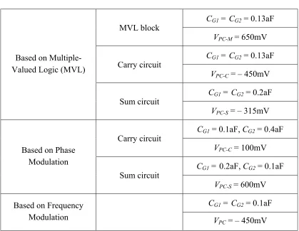
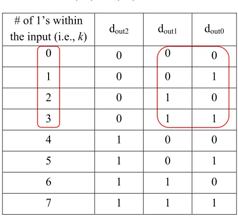
5.1: Input and output relationships of (3:2) and (7:3) counters ... 71
5.2: Parameters for SPICE simulation in Cadence ... 89
5.3: Area-delay-power estimations of the enhanced type phase modulated (3:2) and (7:3) counters ... 95
5.4: Area-delay-power estimations of a 16×16 multiplier using elements in Table 5.3... ... 96
5.5: Area-delay-power estimations of a 16 × 16 multiplier using different technologies .. ... 97
5.6: Temperature and BC performances of single-electron-tunneling based multipliers ... ... 97
List of Abbreviations
ADC Analog-to-Digital Converter
BC Background Charge
BCD Binary-Coded Decimal BDD Binary Decision Diagram
BSIM Berkeley Short-Channel Insulated-gate FET Model CLA Carry Look-ahead Adder
CMOS Complementary Metal-Oxide-Semiconductor
CNT Carbon Nano Tube
CP Charge Pump
CPA Carry Propagation Addition DAC Digital-to-Analog Converter DFC Digital-to-Frequency Converter
EC Electron Counting
FA Full Adder
FDC Frequency-to-Digital Converter
FIB Focused Ion Beam
FSR Frequency Synthesizer
ITRS International Technology Roadmap for Semiconductors LPF Low Pass Filter
MAJ Majority Gate
MC Monte Carlo
ME Master Equation
MOSFET Metal-Oxide-Semiconductor Field-Effect Transistor MVL Multiple-Valued Logic
NTT Nippon Telegraph and Telephone PADOX Pattern Dependent Oxidation
PDP Power-Delay-Product
PFD Phase Frequency Detector
PLL Phase-Locked Loop
PPA Partial Product Accumulation PPG Partial Product Generation PTL Pass-Transistor Logic RCA Ripple Carry Adder
RNG Random-Number Generator
SED Single-Electron Device
SEEL Single-Electron-Encoded Logic SET Single-Electron Transistor SIMON Simulation Of Nanostructures
SOI Silicon-On-Insulator
SPICE Simulation Program with Integrated Circuit Emphasis SRAM Static Random-Access Memory
STM Scanning Tunneling Microscope TLG Threshold Logic Gate
List of Symbols
Notation Definition
⎣ ⎦
⋅ Floor functione Fundamental charge of an electron, e≈ 1.6 × 10⁻¹⁹ C
kB Boltzmann’s constant, kB≈ 1.38 × 10⁻²³ J/K
h Planck’s constant, h≈ 6.63 × 10⁻³⁴ J·s
EC Electron charging energy
Ek Electron kinetic energy
τt Time taken by an electron tunneling through a junction
RT Tunnel junction resistance
CT Tunnel junction capacitance
CG Gate capacitance of SET
CΣ Total device capacitance on the island of SET with respect to ground
Cgdo
Cgso Gate-drain and gate-source overlap capacitances per unit gate width
Cgdl
Cgsl Gate-drain and gate-source overlap capacitances per unit gate length
tox Gate oxide thickness
Vtho Threshold voltage for the long channel device at zero VDS
T Absolute temperature
Chapter 1
Introduction
1.1
Motivations
The scaling-down of the size of MOS transistors according to Moore's law – the
number of transistors on a chip doubles about every two years – has taken place for the
last 40 years, and pushed today’s CMOS technology towards the sub-50nm regime [1]
(Moore's law has been adjusted around 2001 to reflect the realities of integrated circuits,
and currently it states that the number of transistors is going to increase about 1.3 times
every two years). However, MOSFET cannot be shrunk beyond certain limit. The
International Technology Roadmap for Semiconductors (ITRS) [2] stated that “we have
reached the point where the horizon of the roadmap challenges the most optimistic
projections for continued scaling of CMOS.” While some advanced technologies, such as
high-k dielectric, metal gate, or ultrathin silicon-on-insulator (SOI) film, may extend
CMOS lifetime, 10nm gate length is labelled as the showstopper region where CMOS is
going to face some fundamental limits, such as quantum limit. In order to continue the
fascinating performance of CMOS scaling, various nanotechnologies have been
1.2
Single-Electron-Tunneling Technology
Single-electron-tunneling technology [3] is among the most promising candidates for
next-generation electronics which allows the control of a single electron or a small
number of electrons. A basic element of this technology is the tunnel junction which can
be used to build many different single-electron devices (SEDs), such as single-electron
box, single-electron pump, single-electron trap, and so on. Single-electron transistor (SET)
[4] is a special type of SED which is featured by its extremely-small size, ultra-low
power dissipation, and unique Coulomb blockade oscillation characteristic. By utilizing
such novel characteristics of SET, one is able to realize new functionalities with less
number of devices.
In contrast to CMOS technology where current flows continuously, the charge
transport in a SET is discretely controlled by the tunnel junction. Electrons are considered
to tunnel through a tunnel junction strictly one after another.
SET itself exhibits some intrinsic drawbacks, such as low current drivability, small
voltage gain, and low temperature operation. Studies have shown that MOSFET and SET
are rather complementary. Hybrid MOS and SET architectures which combine the merits
of both MOSFET and SET promise to be a much practical implementation for
nanometre-scale circuit design [5].
1.3
Research Objectives
The work presented in this thesis has three objectives:
1. To design arithmetic circuits, including adders and multipliers, using hybrid MOS
2. To further reduce circuit area and power dissipation by utilizing SET’s unique
Coulomb blockade oscillation characteristic.
3. To improve the reliability of SET-based circuits against background charges (BCs)
by using different circuit structures.
It is desirable to design adders and multipliers using hybrid MOS and SET
architectures which are able to dramatically reduce the circuit area and power dissipation.
While it is straightforward to design these circuits following conventional CMOS design
styles, they do not utilize the potential benefits offered by the SET. By using the unique
Coulomb blockade oscillation characteristic (i.e., the periodic I-V curve of SET), new
functionalities can be effectively achieved with less number of devices through novel
design methodologies.
Since BCs (i.e., undesirable fractional charges on the island of SET induced by the
defects or impurities located within the oxide barriers) create serious problem for
SET-based circuits [6], people working at different abstraction levels (i.e., device level, circuit
level, and system level) are trying to find solutions to deal with this effect. As the circuit
designers, we need to build robust circuits that are able to work properly with certain
tolerance against BCs.
1.4
Thesis Organization
This thesis is organized as follows. Chapter 2 introduces the background of
single-electron transistor (SET). It starts with the introduction of the related physics and theory of
single-electron-tunneling technology. Then the structure of SET and its unique Coulomb
how single electrons transport in a SET. This chapter also addresses some important
aspects associated with the SET, including simulation techniques, applications, and
fabrications. Since Coulomb blockade oscillation is the most important characteristic of
SET which is utilized throughout the research work, a variety of simulations using
SIMON simulator are introduced at the end of this chapter. The results are used as the
basic principles that guide the design of more complex circuits.
Chapter 3 discusses the hybrid MOS and SET architectures. This chapter first
introduces a simulation technique used to co-simulate MOSFET and SET, and then
analyzes the performance of two typical SET/MOS hybrid architectures –– serial
SETMOS and parallel SETMOS –– in terms of power dissipation, current driveability,
and temperature effect. An adaptive feedback structure is also introduced in order to
increase the circuit robustness against BCs. A SET/MOS hybrid analog-to-digital
converter (ADC) is demonstrated as an example.
Chapter 4 deals with the design of 1-bit binary full adder (FA), and provides three
different implementations using modified SET/MOS hybrid architectures based on the
schemes of multiple-valued logic (MVL), phase modulation and frequency modulation.
The proposed FA fully utilizes the Coulomb blockade oscillation characteristic of SET and
hence consumes less number of devices and power. The frequency modulated FA exhibits
the high immunity against BCs and can be used to build multi-bit FAs.
Chapter 5 focuses on the design of binary tree multipliers based on multi-input counters
(or compressors) implemented using SET/MOS hybrid architectures. The structure of the
proposed (3:2) and (7:3) counters is based on the phase modulation scheme presented in
structures to deal with some practical issues associated with the SET-based counters, such
as temperature, BCs, and the operating seed.
Chapter 6 proposes the SET-based frequency synthesis including frequency gain and
frequency mixing, and introduces a novel design methodology for arithmetic operations
based on the frequency modulation scheme (similar to the one used in Chapter 4). The
main idea is to first convert the operands from digital to frequency representation, then
perform arithmetic operations in the frequency domain before converting the result back
to the digital representation. The demand for digital-to-frequency and frequency-to-digital
conversions is driven by the simplicity of doing frequency multiplication and the high
immunity against BCs.
Chapter 2
SET Background
2.1
Single-Electron Scaling
The manipulation of a single electron was first demonstrated at the beginning of last
century, but in solid state circuits it was not implemented until the late 1980s. The
necessary nanofabrication techniques have become available during the past three
decades, and have made possible a new field of solid state physics, single-electronics [7].
Single-electronics allows us to control the movement and position of a single electron
or a small number of electrons. Consider a small conductor (traditionally called an island)
to be electrically neutral (i.e., the number of electrons equals to the number of protons).
Initially, the island does not generate any electric field which can be easily charged by an
electron from the outside. With the net charge on the island of – e (i.e., fundamental
charge of an electron, where e≈ 1.6 × 10⁻¹⁹ C), the resulting electric field (for the island
with the size less than 10nm) repulses the following electrons to be added. Although the
fundamental charge is small at the human scale of things, the electric field (which is
inversely proportional to the square of the island size) is rather strong for
This phenomenon makes it possible to control a single electron in a solid-state structure.
More accurately, we have not isolated a single electron since many other electrons are
still presented. But we are able to add (or remove) electrons to (or from) the island with
single-electron precision [3].
A more adequate measure to quantitatively understand single-electron transfer and
related effects is not the electric field, but the charging energy, which is given by
C
e
E
C=
2/
2
(2.1)where C is the capacitance of the island. Since thermal fluctuations will disturb the
motion of electrons, the minimum charging energy to control an electron is
T
k
E
C>
B (2.2)where kB is Boltzmann’s constant (i.e., kB ≈ 1.38 × 10⁻²³ J/K) and T is the absolute
temperature. This means that the capacitance C has to be smaller than 12aF for the
observation of charging effects at the temperature of liquid nitrogen (77K) and smaller
than 3aF for charging effects to appear at room temperature (300K). This requires the
island size to be smaller than 15nm and 5nm, respectively. To use charging effects for the
deterministic logic, most suggested single-electron devices (SEDs) require even higher
values of EC (factor about 50) in order to avoid thermally-induced random tunneling
events. As a result, for room temperature operation, the minimum feature size of the
island has to be smaller than 1nm [8].
In this size range, the electron kinetic energy (i.e., Ek) becomes substantial. It is very
important to develop SEDs capable of working in this size range with EC >> Ek, thus
2.2
Orthodox
Theory
Orthodox theory [9] of single-electron tunneling provides the unique guiding role in
single-electronics. The theory is developed with the following assumptions:
1) The electron energy spectrum within the island is continuous (i.e. the electron
energy quantization is ignored). Strictly speaking this assumption is valid only if
Ek<< kBT, but it frequently gives an adequate description of observations as soon
as Ek<< EC. It should be mentioned that the electron transfer is discrete, but the
electron energy is continuous. Since we are ignoring any quantization of electron
energy in the island, SEDs cannot be included in the group of “quantum electronic
devices” [10].
2) The time taken by an electron tunneling through the barrier (i.e., τt) is assumed to
be negligibly small in comparison with other time scales (including the interval
between neighboring tunneling events). This assumption is valid for tunnel
barriers used in SEDs of practical interest, where τt ~ 10–15 seconds.
3) Coherent quantum processes consisting of several simultaneous tunneling events
(i.e., co-tunneling) are ignored. This assumption is valid only when the electrons
are well localized in the island [11]. This leads to the requirement that the
resistance (i.e., RT) of all tunnel barriers in the system has to be large enough in
order to effectively suppress the quantum-mechanical uncertainty of the electron
location. According to Heisenberg’s energy uncertainty principle, the minimum
resistance of a tunnel barrier is given by
R
T>
h
e
2≈
26
K
Ω
where h is Planck’s constant (i.e., h ≈ 6.63 × 10⁻³⁴ J·s). Notice that this
relationship is of principal importance for SEDs as a whole which makes it
possible to control a single electron.
With above assumptions to be satisfied, the Orthodox theory is in quantitative
agreement with virtually all the experimental data for systems with metallic conductors
and gives a qualitative description of most results for most semiconductor structures.
The main result of Orthodox theory can be concluded as follows [3]: the tunneling of a
single electron through a particular tunnel barrier is always a random event with a
certain rate which depends solely on the reduction of the free energy of the system as a
result of this tunneling event.
2.3
SET Structure
The basic element of a SET [4] is the tunnel junction. If we consider a piece of
conductor separated by an ultrathin dielectric, the overall structure will behavior as a
tunnel junction, as shown in Figure 2.1 (a). Such arrangement of two conductors with an
insulating layer in between not only has a huge resistance (up to MΩ), but also a finite
capacitance (i.e., at the range of aF). According to the laws of classical electromagnetism,
no current can flow through an insulating barrier; however, from the viewpoint of
quantum mechanics, there is a non-vanishing probability for electrons to pass through it
as long as the barrier is thin enough [12]. Most SEDs can be constructed by placing such
tunnel junctions in series, such as single-electron box [13], single-electron pump [14],
single-electron trap [15], single-electron turnstile [16], and so on, where the transport of
(a)
(b)
Figure 2.1: (a) Structure of a tunnel junction; (b) Structure of a single-electron transistor (SET)
With two tunnel junctions that share a common electrode, known as the island, one
can build a SET, as shown in Figure 2.1 (b), where the gate terminal is capacitively
coupled to the island via a thin dielectric (the left one is the one-gate SET while the right
one is the two-gate SET).
If the source terminal of a SET is connected to the ground, and the drain and gate
terminals are biased to the external voltage sources of VDS, VGS1, and VGS2, respectively
(for a two-gate SET), the potential on the island of SET can be expressed as:
Σ Σ Σ Σ
⋅
−
+
+
=
C
e
k
V
C
C
V
C
C
V
C
C
V
TD DSGS G GS G Island 2 2 1
1 (2.4)
where k is the net number of electrons on the island, CΣ is the total device capacitance of
SET (i.e., CΣ = CG1 + CG2 + CTD + CTS). It is VIsland that determines the voltage across the
two tunnel junctions and hence controls the electron transport.
According to the Orthodox theory, the electron tunneling event from a microscopic
point of view is a stochastic process; however, from a macroscopic perspective, the
current flowing through a SET is a deterministic behavior which depends on different
external voltage or current biasing conditions.
2.4
Coulomb
Blockade Oscillation
For constant voltage or current biased SET, its drain-to-source current or voltage
exhibits an oscillating characteristic with respect to the input gate voltage. This
phenomenon is known as Coulomb blockade oscillation [11], which is the most important
For the Coulomb blockade oscillation to occur, Orthodox theory must be satisfied.
Other than this, SET’s drain-to-source voltage (i.e., VDS) cannot exceed e/CΣ. With e/CΣ <
VDS < 3e/2CΣ, Coulomb blockaderegion no longer exists but Coulomb oscillation remains.
If VDS is further increased, Coulomb oscillation will vanish out and SET functions as a
regular resistor.
To understand how electrons transprot in a SET, assume that initially the charge on the
island is Q, then the electrostatic energy of the system (i.e., E1) can be expressed as
Σ
=
C
Q
E
2
21 (2.5)
Now if an electron tunnels from the source to the island, the total electrostatic energy of
the system will become
(
)
Σ−
=
C
e
Q
E
2
22 (2.6)
According to the Orthodox theory, an electron tunneling event can only take place if it
decreases the total energy of the system. That is
2
0
2
2
22
1
Q
e
C
e
e
Q
E
E
−
=
⋅
−
>
⇒
>
Σ
(2.7)
Since Q = CΣ · |V|, where |V| is the voltage drop across the tunnel junction, we can
conclude that the electron tunneling event is possible only when
Σ
>
C
e
V
Notice that at higher temperature, electron may tunnel through the junction even though
|V| is less than e/2CΣ due to the thermal energy effect. Assume that SET works at near
absolute temperature (i.e., the thermal energy effect is negligible), then the electron
tunneling event in a SET can only happen if |VIsland| > e/2CΣ (i.e., electron tunnels from the
source terminal to the island) or |VDS – VIsland| > e/2CΣ (i.e., electron tunnels from the
island to the drain terminal).
To simplify the explanation, we set VDS equal to e/2CΣ and increase the gate votlage (i.e.,
VGS) from 0 to a considerable positive value. Since VIsland is determined by the external
biasing voltages (refer to (2.4)), VIsland will increase along with VGS. Then from Figure 2.2
(where α = e/2CΣ), we can observe that:
1) When VIsland < α, the voltage drop across both source and drain tunnel juctions is
less than α, hence there is no electron tunneling event happened and SET is in
Coulomb blockade region –– see Figure 2.2 (a).
2) If we increase VGS so that VIsland is greater than α –– see Figure 2.2 (b), one electron
will tunnel from the source terminal to the island. Once an electron enters into the
island, the VIsland is dropped by 2α (from point A to point B). As a result, the voltage
drop across the drain terminal is greater than α, and then one electron tunnels from
the island to the drain terminal. Right after the electron leaves the island, the VIsland
returns back to its original value (from point B to point C) which induces another
electron. In this way, a continuous current path is estabilished between the source
and drain terminals.
3) With the further increase of VGS, VIsland is greater than 2α –– see Figure 2.2 (c),
However, since |VIsland – Vsource| > |Vdrain – VIsland|, from the probability point of view,
electrons have more chance to tunnel from the source terminal to the island than
from the island to the drain terminal. As a result, the net number of electrons on the
island will be increased by one, and the VIsland will be reduced by 2α (from point A
to point B). Like Figure 2.2 (a), the SET again enters into the Coulomb blockade
region.
4) When VIsland > 3α –– see Figure 2.2 (d), VIsland is first dropped by 2α (from point A
to point B) with one more electron residuing on the island. Then similar to Figure
2.2 (b), electrons keep tunneling from the source terminal to the drain terminal
which create a continuous current path.
From above observation, we can infer that the periodicity of electron tunneling current
(i.e., IT) is 2α (i.e., e/CΣ) with respect to VIsland. By differentiating (2.4) (assume there is
only one gate for SET, and VDS and k are constant), we can get that
GS G
Island
V
C
C
V
=
⋅
Δ
Δ
Σ
(2.9)
As a result, the periodicity of IT with respect to VGS is e/CG.
For the current biased SET, the VDS will oscillate with the same periodicity as the IT.
The amplitude of VDS oscillation at near absolute temperature is e/CΣ with the positive and
negative slopes of CG /(CΣ – CTD) and – CG /CTD, respectively. While these values will
attenuate at higher temperature, they can be used as the good estimations to predict SET’s
(a) (b)
(c) (d)
2.5
Simulation Techniques
There are mainly three approaches used to simulate SET-based circuits:
1) Monte Carlo (MC) simulation technique: MC technique [17] is the most popular
approach used to simulate SED-based circuits (including SET which is special type
of SED). MC approach starts with all possible tunneling events, calculates their
probabilities, and chooses one of the possible events randomly using the
probabilities for weighting. This is done many times to simulate the transport of
electrons through the network.
2) Master Equation (ME) simulation technique: ME technique is a description for
the underlying Markov process [18] of electron tunneling from island to island, and
thus the circuit occupies different states. With ME method, one needs the set of all
possible states of the circuit, which are defined by the external voltage sources and
the charge distribution in the circuit.
3) SPICE macro modeling technique: This method models SET’s behaviour using
equivalent circuits based on conventional microelectronic components [19, 20],
such as voltage and current sources, diodes, and resistors. Although this approach is
compatible with SPICE environment, the purely empirical nature makes them not
convenient for the SET-based circuit design.
MC technique is considered to be the most accurate way to find the characteristics of
not only SETs, but any SEDs. Some of the well-known MC simulators are SIMON [21],
MOSES [22], KOSEC [23], and SENECA [24]. At the end this chapter, we will simulate a
constant current biased SET using SIMON simulator so as to examine different parameter
2.6
Background Charge Effect
One of the biggest disadvantages of single-electron-tunneling technology is its large
charge sensitivity. This is good for sensors which can be used to build super sensitive
electrometers. However, for logic applications which work at particular voltage or current
biasing conditions, any trapped charge or the charge movement near the island could
easily change the circuit operating point, and hence produces an error [25]. These
undesirable charges are referred as BCs which are mainly induced by defects or impurities
located within the oxide barriers, and cannot be entirely removed by today’s technology. It
has been measured that BCs on the island of SET vary over a period from a few minutes
to hours, and the variation generally follows Gaussian distribution with the high
probability of being less than ±0.3e [6, 26].
Researchers are trying to find solutions dealing with this problem at different levels:
1) Device level: physicists and chemists are looking for different structures and
materials to fabricate SET with as less BCs as possible.
2) Circuit level: circuit designers try to build robust circuits that are able to tolerant
certain amount of BCs. Notice that BCs only shift the phase of Coulomb blockade
oscillation without changing the amplitude and periodicity, SET-based circuits will
exhibit high immunity against BCs if the information is encoded into the amplitude
or frequency.
3) System level: people at this level try to add certain redundancy into the logic to
tolerant BCs, such as using neural network.
This thesis deals with BCs at the circuit level by using novel circuit configurations and
2.7
Applications
Memory design is the most attractive application of SET due to the fact that one can
achieve extraordinary storage density at an extremely low power consumption by using
SETs. Also, for SET-based memories, several known solutions exist to the effect of BCs
[27]. Many research groups have reported different memory architectures based on SETs
[28, 29], and a 128 MB prototype for giga-scale SET memory has already been
implemented on the silicon wafer [30].
In terms of logic applications, SET is very suitable for the multiple-valued logic (MVL)
design [31]. Because of the Coulomb blockade oscillation characteristic, SET has multiple
threshold voltages (this is in contrast to MOSFET which has single threshold voltage)
which can be directly linked to the MVL operations. MVL functions can be therefore
realized by using SETs with a significant reduction of the number of devices.
2.8
Intrinsic Drawbacks
Despite limitations of low temperature operation and the background charge effect,
SET suffers from low current drivability and small voltage gain. As mentioned before, to
sustain Coulomb oscillation, the drain-to-source voltage of SET cannot exceed 3e/2CΣ.
This results in the biasing current of SET at the range of nA which cannot drive large
capacitive load (say 100aF) at relatively high speed. Also, given the slopes of Coulomb
oscillation (i.e., CG /(CΣ – CTD) and – CG /CTD, respectively), the voltage gain of SET is
normally around (or less than) one. Since MOSFETs have advantages that can compensate
these intrinsic drawbacks of SET, hybrid MOS and SET architecture is considered to be a
Although a complete replacement of MOSFET by SET is unlikely in the near future, it
is true that by combining MOSFET and SET, we can bring out a lot of new functionalities
which cannot be mirrored in pure CMOS technology [32].
2.9
Fabrications
Historically, the research on SET fabrications started with metals and superconductors
[33–35] and then expanded to semiconductors [36]. The reason of using silicon as a base
material for SET fabrication is that we can take advantage of the existing CMOS
fabrication technologies. To fabricate SETs on the silicon wafer faces the following
challenges:
1) Island dimension: the island diameter has to be on the order of 2 ~ 3 nm for
sub-ambient temperature operation (i.e., –150 ºC ~ –50 ºC), and ~1nm for room
temperature. It is very difficult for today’s lithography to isolate a tiny piece of
material with a size of a few nanometers. An alternative to lithography techniques
is needed for fabricating silicon SETs.
2) Batch processing: reproducibility in SET fabrication is very important. A
cost-effective SET fabrication technology should be the one that can be used for batch
processing (like CMOS).
3) Background charge effect: since BCs create serious problem for the proper
operation of SET [26], all the processing steps and materials used should be very
clean in order to avoid charge trapping.
4) Energy quantization effect: quantization effect creates another problem for the
Coulomb blockade oscillation. Among possible approaches to avoid such complex
features might be the use of highly doped silicon nano-wires or the use of charge
injection in silicon nano-crystals deposited on SETs [37].
5) Control of tunnel junction resistance: it is difficult to fabricate the tunnel junction
with the resistance as small as possible which is still larger than 26KΩ for proper
quantum confinement.
Despite so many difficulties, various SET fabrication techniques have been reported.
Pattern Dependent Oxidation (PADOX) technique [38] appears to be a very reliable
technology for fabricating SETs which is first introduced by NTT Research Laboratories.
The process is based on the thermal oxidation of a short silicon wire which is connected to
the wide silicon layers. The initial silicon wire is defined in a very thin silicon-on-insulator
(SOI) layer by electron beam lithography and dry etching, and then it is thermally
oxidized in dry oxygen ambient. A polysilicon gate deposition over the silicon wire
defines the final SET structure. An equivalent island with 7nm diameter is effectively
formed in the silicon wire whose CΣ = 1.5aF. Such small dimensions which are below the
lithographic limit are possible because the size of the remaining silicon is reduced as
oxidation proceeds.
Providing islands with sub-lithographic controlled dimensions is one of the advantages
of thermal oxidation. Another important feature of PADOX is that the gate capacitance
(i.e., CG) of the silicon island shows an almost linear relationship to the designed length of
the silicon wire which makes the reproducible silicon SET fabrication possible.
9 Lithographic point contact [37]: this SET architecture uses the point contact of two
triangular-shaped MOSFETs which are fabricated on SOI wafer using electron
beam lithography and an anisotropic etching technique. The width of the point
contact channel is less than 30nm. Although the tunnel barriers and silicon dots are
not intentionally formed, they are naturally introduced in the channel. Some devices
are found to operate as SETs even at room temperature.
9 Scanning Tunneling Microscope (STM) nano-oxidation [39]: a layer of 3 nm thick
titanium is deposited by evaporation on the thermally oxidized SiO2n-Si substrate.
The Ti surface is oxidized by anodization using the STM tip as a cathode through
the water that adhered to the surface of the Ti from the atmosphere, and oxidized
titanium lines of nanometer size are formed which are used for the formation of the
small island of SET.
9 Focused Ion Beam (FIB) prototyping [40]: this is based on two steps, the first one
consists of preparing a relatively large and long SOI wire connected between two
silicon pads on SOI with a thickness of around 30nm, and the second one is the FIB
treatment which reduces the channel width to a dimension as small as 50nm. The
silicon wire is further oxidized to decrease its size from 30nm to around 15nm in
diameter, and to grow an all-around gate oxide.
9 Sidewall patterning method [41]: this is based on SOI nano-wire processing
combined with an electrostatically defined island where the tunnel barrier are
electrically formed by the sidewall depletion gates. This fabrication process is
interesting because the tunnel barrier and the size of the island are controlled in a
Recent alternatives to silicon SETs are based on carbon nano tubes (CNTs) [42] and
some molecular materials [43, 44]. These new nano materials have the potential to be
co-integrated in or above the silicon CMOS devices. CNTs have also been suggested as the
possible candidates for room-temperate operated SETs [45].
2.10
Case Study: SIMON Simulations
Since Coulomb blockade oscillation is the unique characteristic of SET which can be
utilized to effectively achieve a lot of functionalities with less number of devices through
novel design methodologies, we first of all study this characteristic in detail, and examine
different parameter effects on this characteristic using the SIMON simulator. The results
can be used as the basic principles to guide the design of more complex circuits.
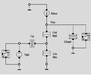
The circuit simulated in the SIMON simulator is shown in Figure 2.3 which is a
constant current biased one-gate SET with a loading capacitor. The parameters used for
the simulations are as follows: RTD = RTS = 1MΩ, CTD = CTS = 1aF (SET’s source and
drain junction resistance and capacitance), CG = 2aF (SET’s gate capacitance), IBias = 2nA
(biasing current), CLoad = 100aF (loading capacitance), T = 1K (operating temperature),
and BC = 0 (background charge on the island of SET).
If increasing VGS from 0 to 80mV, we will get a voltage oscillation at VDS. By changing
the following parameters one at a time, we can observe that:
1) Effect of loading capacitance: with CLoad = 1aF, 10aF, 100aF, and 1fF, respectively,
we get four VDS oscillations, as shown in Figure 2.4. It is observed that when CLoad is
small (i.e., less than 10aF), it will have an effect on the VDS oscillation. The VDS
indicates that when we build large SET-based circuits, interconnected SETs will affect
each other. In order to prevent this effect, a large grounded capacitor (with the
capacitance more than 100aF) needs to be added to the node of interconnected SETs.
2) Effect of biasing current: with IBias increasing from 2nA to 11nA in the step of 3nA,
we get four VDS oscillations, as shown in Figure 2.5. It is observed that as IBias
increases, the level of VDS (i.e., the averaging VDS) increases but the amplitude of VDS
decreases. In order to sustain Coulomb oscillation, IBias for this configuration cannot
exceed 10nA. With further reduced junction resistance and device capacitance, IBias
can be as high as a few hundred nA.
3) Effect of total device capacitance (i.e., CΣ): with CTD = CTS = 1aF, 1.5aF, and 2aF (i.e.,
CΣ = 3aF, 4aF, and 5aF), respectively, we get three VDS oscillations, as shown in
Figure 2.6. It is observed that as CΣ increases, the amplitude of VDS oscillation
decreases (i.e., the maximum VDS decreases but the minimum VDS remains constant).
The amplitude of VDS oscillation is inversely proportional to CΣ which can be
expressed as e/CΣ at near absolute temperature.
4) Effect of input gate capacitance: with CG = 1aF, 2aF, and 3aF, respectively, we get
three VDS oscillations, as shown in Figure 2.7, where we set CTD = CTS = 1.5aF, 1aF,
and 0.5aF (corresponding to the CG of 1aF, 2aF, and 3aF, respectively) so as to
maintain the same CΣ = 4aF (this ensures the same amplitude of VDS oscillation for
better comparison) and increase VGS from 0 to 160mV. It is observed that as CG
increases, the periodicity of VDS oscillation decreases. The periodicity of VDS
5) Effect of temperature: with operating temperature increasing from 1K to 21K in the
step of 10K, we get three VDS oscillations, as shown in Figure 2.8. It is observed that as
the temperature increases, the amplitude of VDS decreases (i.e., the maximum VDS
decreases but the minimum VDS remains constant). In order to sustain Coulomb
oscillation, the operating temperature for this configuration has to be less than 100K.
With further reduced device capacitance (i.e., CΣ < 3aF), SET is able to work at room
temperature.
6) Effect of BCs: with BCs on the island of SET being –0.1e, 0, and 0.1e, respectively,
we get three VDS oscillations, as shown in Figure 2.9. It is observed that BCs only shift
the phase of VDS oscillation without changing its amplitude and periodicity. Positive
BCs shift VDS oscillation to the right while negative BCs move VDS oscillation to the
left. Only fractional BCs will change the phase of VDS oscillation. This observation
indicates that the SET-based circuits will exhibit high immunity against BCs if the
information is encoded into the amplitude or periodicity of this oscillation.
7) Effect of second gate voltage: in order to examine this effect, we add one more gate
for SET with the gate capacitance of 1aF. With the voltage applied on the second gate
of SET (i.e., VGS2) being –100mV, 0, and 100mV, respectively, we get three VDS
oscillations, as shown in Figure 2.10. It is observed that the effect of VGS2 is the same
as the effect of BCs (i.e., only shift the phase of VDS oscillation without changing its
amplitude and periodicity). Positive VGS2 shifts VDS oscillation to the left while
negative VGS2 moves VDS oscillation to the right. This observation implies that one is
able to offset the effect of BCs by applying appropriate voltage through an additional
Figure 2.3: Constant current biased SET in SIMON simulator environment.
Figure 2.5: Effect of IBias on VDS oscillation, where IBias= 2nA, 5nA, 8nA, and 11nA.
Figure 2.7: Effect of CG on VDS oscillation, where CG = 1aF, 2aF, and 3aF.
Figure 2.9: Effect of BCs on VDS oscillation, where BC = – 0.1e, 0, and 0.1e.
Chapter 3
SET
/
MOS Hybrid Architectures
3.1
Introduction
SET is considered to be a promising candidate for further VLSI design because of its
nanometer-scale feature size, ultra-low power dissipation, and unique Coulomb blockade
oscillation characteristic. Unfortunately, circuits with pure SETs have very limited
applications due to the low current drivability, small voltage gain and low temperature
operation. Study shows that MOSFET and SET are rather complementary. Since
MOSFET has advantages such as high-speed driving and high voltage gain that can
compensate for the intrinsic drawbacks of SET, hybrid MOS and SET architectures,
which combine the merits of both MOSFET and SET, promise to be a more practical
implementation for nanometer-scale circuit design [32]. With hybrid circuits, a lot of new
functionalities can be achieved with less number of devices which cannot be mirrored in
pure CMOS technology.
In this chapter, we first introduce the MIB compact mode which can be used to
co-simulate MOSFET and SET. Then we co-simulate and compare two typical SET/MOS
drivability and the temperature effect. Since BCs create serious problem on the circuit
performance, we propose an adaptive feedback structure which dramatically increases the
robustness of hybrid circuits against BCs. An improved SET/MOS hybrid
analog-to-digital converter (ADC) is also presented as an example which takes advantage of the
proposed feedback structure.
3.2
Hybrid MOS and SET Co-Simulation
MC technique is considered to be the most accurate method to simulate SED-based
circuits (including SET) which is based on probability calculation. However, this method
takes very long time if the circuit becomes large and cannot be used to co-simulate with
MOSFETs. For example, each simulation conducted at the end of Chapter 2 using
SIMON simulator takes more than three minutes (based on a general personal computer),
and there are only components of tunnel junctions, resistors, capacitors, and voltage and
current sources that can be used to build large circuits.
MIB (named after three authors [46]) compact model of SET achieves very fast
simulation speed. The model is developed using ME technique and has been verified with
perfect match to the MC result. The Verilog-A version of this model can be easily
integrated into a conventional SPICE simulator through the Verilog-A interface [47].
MIB model is founded on the following assumptions:
1) It obeys Orthodox theory of single-electron tunneling;
2) The interconnect capacitances associated with gate, source, and drain terminals are
much larger than the device capacitances (i.e., CTD, CTS, CG, or CG2), which ensures
that the total device capacitance with respect to ground (i.e., CΣ) equals to the
Remember the simulation conducted at the end of Chapter 2 where the small loading
capacitance has an effect on the actual SET characteristic. In fact, in a circuit where many
SETs are connected to each other, CΣ of any SET not only depends on its own device
capacitances but also on the parameters of other SETs. This difficulty can be solved if the
second assumption holds true. For hybrid MOS and SET circuits, because the
interconnect capacitance between MOSFET and SET (via connection lead) is much
larger than SET’s device capacitances (a few aF at most), the second assumption appears
to be very practical.
MIB compact model not only integrates device capacitances and resistances but also
temperature and BCs as the model parameters which is very attractive for hybrid MOS
and SET co-simulation [48].
In the following of the thesis, we use MIB compact model for SETs along with
BSIM3v3 (for CMOS 180nm technology) and BSIM4 (for CMOS 65nm technology)
Spector models for MOSFETs. The hybrid MOS and SET co-simulations are conducted
using conventional Spector simulator in Cadence analog environment.
3.3
Serial and Parallel SETMOS
There are two widely used hybrid MOS and SET architectures, one is SET and
MOSFET connected in serial biased by one current source, and the other is SET and
MOSFET connected in parallel biased by two current sources, as shown in Figure 3.1. In
the remainder of the thesis, they are called serial SETMOS and parallel SETMOS,
(a) (b)
Figure 3.1: (a) Serial SETMOS; (b) Parallel SETMOS.
The serial SETMOS structure is first proposed by Inokawa et al. [31] and has been
used as the basic building block to construct many functional circuits, such as static
random-access memory (SRAM) [31], analog-to-digital converter (ADC) [31, 49],
random-number generator (RNG) [50], voltage-controlled oscillator (VCO) [51], and so
on. The parallel SETMOS structure is first introduced by Mahapatra et al. [46–48] which
![Figure 2.2: Electron tunneling mechanisms in the SET. (Reproduced with permission from [32])](https://thumb-us.123doks.com/thumbv2/123dok_us/1443380.1176833/36.612.109.551.105.640/figure-electron-tunneling-mechanisms-set-reproduced-permission.webp)