CSEIT172289 | Received : 10 May 2017 | Accepted : 20 May 2017 | May-June-2017 [(2)3: 306-308]
International Journal of Scientific Research in Computer Science, Engineering and Information Technology © 2017 IJSRCSEIT | Volume 2 | Issue 3 | ISSN : 2456-3307
306
Digital Bin Receptacle
Srishti Sinha, Neha Singh, Mayuri Agrawal, Tomeshwari Sahu, Shubham Sharma,
Shailendra Singh
Department of Electronics and Telecommunication, RSR Rungta College of Engineering & Technology Bhilai, Chhattisgarh, Punjab, India
ABSTRACT
In our city many times we see that the garbage bins or dustbins placed at public places are overflowing. It creates unhygienic conditions for people. Also it creates ugliness to that place. At the same time bad smell is also spread. To avoid all such situations we are going to implement a project called Garbage collection bin overflow indicator using GSM technology. In this project we are going to place a weight sensor under the dustbin. When the weight reaches to the threshold value, a sms will be sent to the respective Municipal / Government authority person. Then that person can send the collection vehicle to collect the full garbage bins or dustbins. We have observed that the municipal officer or the government authorized person will monitor the status of dustbin. Or generally we see that they have a regular schedule of picking up these garbage bins or dustbins. This schedule varies as per the population of that place. It can be once in a day or twice in a day or in some cases once in two days. However we see that in case there is some festival or some function, lots of garbage material is generated by people in that particular area. In such cases the garbage dustbin gets immediately full and then it overflows which creates many problems. So in situations, with help of our project the government authority person can get SMS immediately. So they will get SMS before their periodic interval visit of picking up the dustbin. Then they can go and pick up the dustbins.
Keywords : SMS, FeCl, MOS, AT89S52, LED, VACANT, LCD
I.
INTRODUCTION
Waste management is the collection, transport, processing or disposal, managing and monitoring of waste materials. The term usually relates to materials produced by human activity, and process is generally under taken to reduce their effect on health, the environment or aesthetics. It is the distinct practice from the resource recovery which focuses on delaying the rate of consumption of natural resources. All waste materials, whether they are solid, liquid, gaseous or radioactive fall within the remit of waste management.
Waste management practices can differ for developed and developing nations, for urban and rural areas, and for residential and industrial producers. Management of non hazardous waste, residential and institutional waste in metropolitan areas is usually the responsibility of local government authorities, while management for non hazardous commercial and industrial waste is usually the responsibility of the generator subject to local, national or international authorities. Solid waste
policy in India specifies the duties and responsibilities for hygienic waste management cities and citizens of India. This policy was framed in September 2000, based on the March 1999 report of the committee for solid waste management in class 1 cities of India to the Supreme court, which urged statutory bodies to complaint with the report’s suggestions and recommendations. These also serve as a guide on how to comply with the MSW rules. Both the report and the rules, summarized below, are based on the principle that the best way to keep streets clean is not to dirty them in the first place. So a city without street bins will ultimately become clean and state clean. They advocate daily doorstep collection of “wet” (food) waste for composting, which is the best option for India. This is not only because composting is a cost effective process practiced since Vedic times, but also because India’s soils need organic manure to prevent loss of fertility through unbalanced use of chemical fertilizers.
The task performed step by step are as
follows:-2.1 PCB DESIGNING 2.1.1 P.C.B. LAYOUT
The entire circuit can be easily assembled on a general purpose P.C.B. board respectively. Layout of desired diagram and preparation is first and most important operation in any printed circuit board manufacturing process. First of all layout of component side is to be made in accordance with available components dimensions.
2.1.2 PREPARING CIRCUIT LAYOUT
First of all the actual size circuit layout is to be drawn on the copper side of the copper clad board. Then enamel paint is applied on the tracks of connection with the help of a shade brush. We have to apply the paints surrounding the point at which the connection is to be made. It avoids the disconnection between the leg of the component and circuit track. After completion of painting work, it is allowed to dry.
2.1.3 DRILLING
After completion of painting work, holes 1/23inch(1mm) diameter are drilled at desired points where we have to fix the components.
2.1.4 ETCHING
The removal of excess of copper on the plate apart from the printed circuit is known as etching. From this process the copper clad board with printed circuit is placed in the solution of FeCl with 3-4 drops of HCL in it and is kept so for about 10 to 15 minutes and is taken out when all the excess copper is removed from the P.C.B.
After etching, the P.C.B. is kept in clean water for about half an hour in order to get P.C.B. away from acidic, field, which may cause poor performance of the circuit. After the P.C.B. has been thoroughly washed, paint is removed by soft piece of cloth dipped I thinner or turbine. Then P.C.B. is checked as per the layout, now the P.C.B. is ready for use.
2.1.5 SOLDERING
Soldering is the process of joining two metallic conductor the joint where two metal conductors are to be join or fused is heated with a device called soldering iron and then as allow of tin and lead called solder is applied which melts and converse the joint. The solder cools and solidifies quickly to ensure is good and
durable connection between the jointed metal converting the joint solder also present oxidation.
2.1.6 SOLDERING AND DESOLDERING TECHIQUES:
These are basically two soldering techniques.
Manual soldering with iron. Mass soldering.
2.1.7 SOLDERING WITH IRON
The surface to be soldered must be cleaned & fluxed. The soldering iron switched on and bellowed to attain soldering temperature. The solder in form of wire is allied hear the component to be soldered and heated with iron. The surface to be soldered is filled, iron is removed and joint is cold without disturbing.
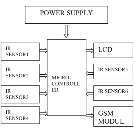
2.2BLOCK DIAGRAM
Figure 1. Smart Dustbin
2.3 WORKING 2.3.1. IR SENSOR
Infrared technology addresses a wide variety of wireless applications. The main areas are sensing and remote controls. In the electromagnetic spectrum, the infrared portion is divided into three regions: near infrared region, mid infrared region and far infrared region.
The frequency range of infrared is higher than microwave and lesser than visible light.
MICRO-Figure 2. IR Receiver & Transmitter
2.3.2. LIQUID CRYSTAL DISPLAY
This is the first interfacing example for the Parallel Port. We will start with something simple. This example doesn't use the Bi-directional feature found on newer ports, thus it should work with most, if not all Parallel Ports. It however doesn't show the use of the Status Port as an input for a 16 Character x 2 Line LCD Module to the Parallel Port. These LCD Modules are very common these days, and are quite
simple to work with, as all the logic required running them is on board.
Figure 3. Pin description of LCD
2.3.3. VOLTAGE REGULATOR
Voltage regulator ICs are available with fixed (typically 5, 12 and 15V) or variable output voltages. The maximum current they can pass also rates them. Negative voltage regulators are available, mainly for use in dual supplies. Most regulators include some automatic protection from excessive current (over load protection) and overheating (thermal protection). Many of fixed voltage regulator ICs has 3 leads. They include a hole for attaching a heat sink if necessary.
Figure 4. Voltage Regulator
2.3.4. POWER SUPPLY
The circuit uses standard power supply comprising of a step-down transformer from 230V to 12V and 4 diodes forming a bridge rectifier that delivers pulsating dc which is then filtered by an electrolytic capacitor of
about 470µF to 1000µF. The filtered dc being unregulated, IC LM7805 is used to get 5V DC constant at its pin no 3 irrespective of input DC varying from 7V to 15V. The input dc shall be varying in the event of input ac at 230volts section varies from 160V to 270V in the ratio of the transformer primary voltage V1 to secondary voltage V2 governed by the formula V1/V2=N1/N2. As N1/N2 i.e. no. of turns in the primary to the no. of turns in the secondary remains unchanged V2 is directly proportional to V1.Thus if the transformer delivers 12V at 220V input it will give 8.72V at 160V.Similarly at 270V it will give 14.72V.Thus the dc voltage at the input of the regulator changes from about 8V to 15V because of A.C voltage variation from 160V to 270V the regulator output will remain constant at 5V.
The regulated 5V DC is further filtered by a small electrolytic capacitor of 10µF for any noise so generated by the circuit. One LED is connected of this 5V point in series with a current limiting resistor of 330Ω to the ground i.e., negative voltage to indicate 5V power supply availability. The unregulated 12V point is used for other applications as and when required.
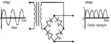
2.3.5. BRIDGE RECTIFIER
A rectifier is an electrical device that converts
alternating current
(AC), which periodically reverses direction, todirect current
(DC), current that flows in only one direction, a process known as rectification. Rectifiers have many uses including as components ofpower supplies
and asdetectors
ofradio
signals. Rectifiers may be made ofsolid statediodes
,vacuum
tube
diodes,mercury arc valves
, and other components. The output from the transformer is fed to the rectifier. It converts A.C. into pulsating D.C. The rectifier may be a half wave or a full wave rectifier. In this project, a bridge rectifier is used because of its merits like good stability and full wave rectification.2.3.6. FILTER
Capacitive filter is used in this project. It removes the ripples from the output of rectifier and smoothens the D.C. Output received from this filter is constant until the mains voltage and load is maintained constant. However, if either of the two is varied, D.C. voltage received at this point changes. Therefore a regulator is applied at the output stage.
2.3.7. MICROCONTROLLER
The AT89S52 is a low-power, high-performance CMOS 8-bit microcontroller with 8K bytes of in-system programmable Flash memory. The device is manufactured using Atmel’s high-density non volatile memory technology and is compatible with the industry standard 80C51 instruction set and pin out. The on-chip Flash allows the program memory to be reprogrammed in-system or by a conventional non volatile memory programmer. By combining a versatile 8-bit CPU with in-system programmable Flash on a monolithic chip, the Atmel AT89S52 is a powerful microcontroller which provides a highly-flexible and cost-effective solution to many embedded control applications.
2.3.8. TRANSFORMER
Transformer is a major class of coils having two or more windings usually wrapped around a common core made from laminated iron sheets. It has two cols named primary and secondary. If the current flowing through primary is fluctuating, then a current will be inducted into the secondary winding. A steady current will not be transferred from one coil to other coil.
Figure 4. Transformer
2.3.9. DIODE
The diode is a p-n junction device. Diode is the component used to control the flow of the current in any one direction. The diode widely works in forward bias.
Figure 5. Diode Symbol
When the current flows from the P to N direction. Then it is in forward bias. The Zener diode is used in reverse bias function i.e. N to P direction. Visually the identification of the diode`s terminal can be done by identifying he silver/black line. The silver/black line is the negative terminal (cathode) and the other terminal is the positive terminal (cathode).
2.3.10. RESISTORS
A resistor is a two-terminal electronic component designed to oppose an electric current by producing a voltage drop between its terminals in proportion to the current, that is, in accordance with Ohm's law:
V = IR
Resistors are used as part of electrical networks and electronic circuits. They are extremely commonplace in most electronic equipment.
Figure 6. Resistors
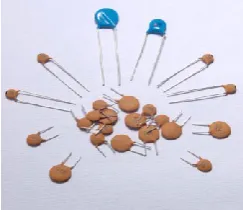
2.3.11. CAPACITORS
A capacitor or condenser is a passive electronic component consisting of a pair of conductors separated by a dielectric. When a voltage potential difference exists between the conductors, an electric field is present in the dielectric. This field stores energy and produces a mechanical force between the plates. The effect is greatest between wide, flat, parallel, narrowly separated conductors..
2.3.12. LED
LEDs are semiconductor devices. When current passes through the LED, it emits photons as a byproduct. Normal light bulbs produce light by heating a metal filament until it is white hot. LEDs produce photons directly and not via heat, they are far more efficient than incandescent bulbs.
Figure 7. Typical LED Figure 8. circuit symbol
2.4 GSM/GPRS MODULE
GSM/GPRS module is used to establish
communication between a computer and a
GSM-GPRS system. Global System for Mobile
communication (GSM) is an architecture used for
mobile communication in most of the countries. Global
Packet Radio Service (GPRS) is an extension of GSM
that enables higher data transmission rate. GSM/GPRS
module consists of a GSM/GPRS modem assembled
together with power supply circuit and
communication interfaces (like RS-232, USB, etc) for
computer.
Figure 8. GSM MODULE
III.
RESULT
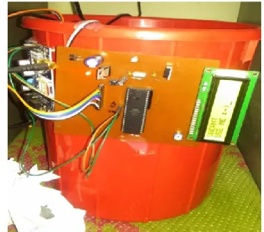
With due course of time we have successfully achieved what we really wanted to design.
Here is the pictorial representation of our running project.
MODE 1- VACANT
During the working if dustbin is VACANT and it will shows vacant in LCD. The demo is shown below.
Figure 9. VACANT POSITION OF DUSTBIN
MODE 2: WHEN DUSTBIN IS ON FULL CONDITION
When the dustbin is full then it will display on LCD as shown below:-
Figure 9. FULL POSITION OF DUSTBIN
IV.
CONCLUSION
corporation water tank overflowing maintenance, road traffic maintenance.
V.
REFERENCES
[1]. Pavithra, “Smart Trash System: An Application Using ZigBee” in IJISET- International Journal of Innovative Science, Engineering & Technology, Volume-1, Issue-8, October 2014 [2]. Twinkle Sinha, K Mugesh Kumar & P Saisharan,
“Smart Dustbin” in IJIEEE-International Journal 0f Industrial Electronics & Electrical Engineering, Volume-3, Issue-5, May 2015 [3]. A Survey on Smart Garbage Management in
Cities using IoT Ruhin Mary Saji1, Drishya Gopakumar2, Harish Kumar S3 , K N Mohammed Sayed4, Lakshmi s5
[4]. National Conference on Product Design (NCPD 2016), July 2016