ABSTRACT
Yoganand N Saripalli. Growth, Characterization and Device Processing of GaN Metal Oxide Semiconductor Field Effect Transistor (MOSFET) Structures. (Under the supervision of Dr M.A.L. Johnson)
The physical properties of GaN, high saturation velocity, high breakdown fields, high electron mobility, wide bandgap energy and high thermal conductivity, make it a promising material for field effect transistor (FETs) devices for high speed, high power, and small channel length applications. Despite the success of GaN electronic devices such as heterojunction field effect transistors (HFETs), fabrication of GaN Metal Oxide Semiconductor (MOS) transistors remains a technical challenge. The primary reason for this is the non-availability of a gate dielectric with a low density of interface states and the simultaneous requirement of ohmic source/drain contacts which are compatible with enhancement mode structures. Unlike existing III-N HFET devices, which have a high free carrier density two dimensional electron gas (2DEG) in the semiconductor substrate, a MOSFET in either accumulation or inversion mode requires low free carrier concentration in the semiconductor channel, and a high density of free carriers in adjacent source and drain areas. This research explores the development, and demonstration of an enhancement mode (normally off) GaN MOSFET with highly doped source/drain ohmic contacts and compatible gate dielectric.
Growth, Characterization and Device Processing of GaN Metal
Oxide Semiconductor Field Effect Transistor (MOSFET) Structures
By
Yoganand N Saripalli
A Dissertation Submitted to the Graduate Faculty of North Carolina State University
In partial Fulfillment of the
Requirements for the Degree of Doctoral of Philosophy In
Materials Science and Engineering Raleigh
2005
APPROVED BY:
J.F. Muth D.W. Barlage
Biography
Yoganand Saripalli was born to Prabhakara Rao and Sita Saripalli in Kakinada,
India on January 19
th, 1978. He studied in Visakhapatnam, where he graduated from Sri
Satya Sai Vidya Vihar high school in 1995. Upon graduation from high school, he
enrolled at Andhra University, Visakhapatnam, India, where he received a Bachelor of
Engineering Degree in Metallurgical Engineering. Upon graduation from Andhra
University in May 1999, he attended the North Carolina State University, where he
received a Master of Science degree (M.S) in Materials Science and Engineering. He
completed the M.S. degree in the Spring of 2002, with a Masters thesis in
“
Integrated
AlN/diamond heat spreaders for silicon device processing”
under the supervision of Dr
Acknowledgements
I owe the credit for accomplishment in my doctoral research to Dr Johnson for
being a superb advisor and a role model. He always stood by me during stressful times,
both on the professional and personal fronts. I must say that I was very fortunate to have
worked under his supervision. But for his guidance and support, I would not have been
able to accomplish the challenging research tasks I was faced with time and again during
my research. I would also like to thank Dr D.W. Barlage for being the co-advisor and
providing the necessary support and inputs during the course of my work. I thank Dr
Duscher for being in my committee, his critical reviews of my work, and greatly indebted
to his TEM group: Lirong, Trinity, Fude and Donovan, for helping me characterize my
device structures and getting the crucial results that allowed to me graduate eventually!
Dr. Muth has always been supportive since my early days of research in the Photonics
Lab. He has given me several valuable inputs during my research and guided me during
some crucial and much needed moments during my research. I am thankful to him for
being in my committee and being supportive throughout my stay in the photonics lab. I
thank Dr Sitar for his critical review of my work, his keen questions and inputs that have
broadened the scope of my work, and his intellectually stimulating courses.
thank the personnel from the company, Kymatech in Raleigh for performing X-ray
diffraction studies and research collaboration. I am duly indebted to all these
collaborators but for whom my research would have not been smoothly accomplished.
My research in the lab would not have been possible without the friendly
colleagues who were always supportive and guided me during my early days of MOCVD
operation and learning. Thanks to Xing-Quan Liu, J.P. Long, Andrew Oberhofer, Ailing
Cai, and Christian Mion. Special thanks to Joe Matthews who taught most of the lab
practices, shared my frustrations at work and guided me through the entire course of my
research. Chang Zeng, thanks a lot for the dielectric depositions in our lab and the device
processing. Krish Dandu and Yawei Jin: thanks a lot guys for the electrical device
characterization and providing me with the most important results that helped me
graduate! I also enjoyed training the more recent graduate students, Judy and Ginger and
enjoyed their company in research. Good luck and the all the very best to you both in
fulfilling your research goals.
There are many more important people whom I am always indebted to for making
my life in the United States comfortable and enjoyable. Edna Deas for leading me
through the department formalities and for being there whenever I needed any
professional help with department, Dr Jag Kasichainula for introducing me into the world
of research. I thoroughly enjoyed my stint as a graduate student under him. He was the
one who sowed the seeds of research in me during my tenure as a Master’s student. I owe
Thanks a lot to the large circle of my friends who kept my life sane and enjoyable
beyond outside my PhD life. Lakshmi Nittala, Prabhakar, Sridhar Rao, Shiva Prasad,
Mayank bhai, Arin, Ajith, Sandeep, Manav, Debasmith, Arghya, Lakshmi, Shruti, my
room mates-Bobby, Sai, Manoj, Ramesh, and colleagues in Materials Science
department-Nirmal, Amit, Abhishek, Sivaraman, Vikram and Koti, and all the members
of Hindu Students Council at NC State who have always been there for me and teaching
me the meaning of a fulfilling life. Thanks a lot guys! I would’ve not made it this far
without you all.
Finally I bow in all due respect to the first Gurus of my life, my parents, brother
and sister, and extended family members for being so caring and their constant support
and encouragement throughout my graduate study. At this moment I would also like to
remember my teachers from kindergarten to my graduate study for having taught me and
for having been the Gurus and guiding light of my life. Finally, I am grateful to my love
and fiancée Sailaja for being there when I needed her the most and sharing all my
TABLE OF CONTENTS
LIST OF TABLES---xi
LIST OF FIGURES---xii
1.
Historical Background on GaN Metal Oxide Semiconductor Field Effect
Transistor (MOSFET) ---1
1.1
Prologue to Thesis---1
1.2
Introduction---2
References---6
2.
Background on Material and Device Technology---10
2.1
Metal Semiconductor Contacts---10
2.1.1
Schottky Contacts---11
2.1.2
Ohmic Contacts---12
2.1.3
Electron Transport Mechanisms Between a Metal and
Semiconductor---14
2.2
Metal Oxide Semiconductor MOSFET and Device Scaling---16
2.2.1
Modern Trends in MOSFETs and Scaling Rules---22
2.2.2
MOSFET Substrate Advances---24
2.2.3
Reduced MOSFET Dimensions---25
2.2.4
Summary of Existing Research---25
2.3
Choice of New Materials and MOSFET Channel---26
2.4
Summary---28
References---30
3.
Development and Current Status of GaN and III-N Materials Research
3.1
Introduction---42
3.1.1
Metalorganic Chemical Vapor Deposition---43
3.1.2
MOCVD
Growth
Process
of
GaN:
Chemistry
and
Thermodynamics---44
3.1.3
Thermodynamics and Kinetics of Nucleation and Surface
Diffusion---46
3.2
Growth of GaN Thin films---52
3.2.1
The Low Temperature Buffer Layer---53
3.2.2
Misfit Stress and Dislocations---59
3.2.3
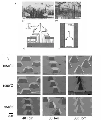
Epitaxial Lateral Overgrowth and Selected Area Growth---63
3.2.3.1
Mechanism of Epitaxial Lateral Overgrowth---65
3.2.4
Selected Area Growth---67
3.2.4.1
Model for Selected Area Growth---69
3.2.4.2
Selected Area Mass Transport Regrowth---71
3.3
Electronic Properties: Doping GaN---71
3.3.1
p-type Doping in GaN---72
3.3.2
n-type Doping in GaN---73
3.5.2
GaN Field Effect Transistors---80
3.5.2.1
GaN MOSFETs---83
3.5.2.2
GaN MOSFETs Summary---85
3.6
Characterization Techniques---86
3.6.1
Optical Characterization---86
3.6.2
Atomic Force Microscopy---87
3.6.3
Thickness Measurement by Dektak Profilometry---88
3.6.4
Scanning electron Microscopy and Cathodoluminescence---89
3.6.5
Transmission Electron Microscopy and Electron Energy Loss
Spectroscopy---90
3.6.6
Secondary Ion Mass Spectroscopy (SIMS)---91
3.6.7
Micro-Raman Spectroscopy---92
References---94
4.
Properties of III-N MOS Structures with Low Temperature Epitaxially
Re-grown Ohmic Contacts---120
Abstract---121
Introduction---122
Experimental Details---122
Results and Discussion---123
Conclusions---126
References---127
Appendix 4A: Summary of Re-growth Design of Experiments---134
References 4A---137
5.
Transmission Electron Microscopy Study of an Epitaxial Gate Oxide on
III-N Semiconductor Structures---140
Abstract---141
Introduction---141
Experimental Details---142
Results and Discussion---143
Conclusions---146
References---147
6.
Transmission Electron Microscopy Studies of Re-grown GaN Ohmic
Contacts on Patterned Substrates for MOSFET Applications---152
Abstract---153
Introduction---154
Experimental Details---155
Results and Discussion---156
Conclusions---158
References---160
Conclusions---175
References---176
8.
Device Results---182
Introduction---183
Experimental Details---183
Results and Discussion---185
Conclusions---187
References---189
Appendix 8A: GaN MOSFET Device Fabrication Process Flow----193
9.
Conclusions and Future Work---198
9.1
Summary and Conclusions---198
9.2
Future Work---201
9.2.1
Surface and Regrowth Studies---201
9.2.2
Epitaxial Lateral Overgrowth of Doped Ohmic Regions---202
9.2.3
Growth on R-Plane---203
9.2.4
Simultaneous Growth of N and Ga Polar Regions to fabricate
MOSFETs and CMOS structures---203
9.2.5
Growth on Native GaN Substrates---204
9.2.6
Dielectric Studies---204
9.2.7
Device Engineering---204
9.3 Conclusion and GaN MOSFET Opportunity---204
LIST OF TABLES
Table1.1 Electronic Properties of Various Semiconductors---8
Table3.1 Properties of GaN and Related Substrates Used for GaN Epitaxy---119
Table3.2 Electrical Properties of potential dielectrics used in GaN MOSFETs---119
Table7.1 Measured Raman Mode Frequencies and their FWHMS---178
LIST OF FIGURES
1. Historical Background on GaN Metal Oxide Semiconductor Field Effect
Transistor (MOSFET)
1.
The Power-Frequency Map---8
2.
Combined Figure of merit---9
2. Background on Material and Device Technology
2.1
Schottky and Ohmic Contacts---34
2.2
(a) Schottky Contact with
Φ
m>
Φ
sfor an n-type semiconductor (b) Ohmic
Contact with
Φ
m<
Φ
sfor an n-type semiconductor---34
2.3
Electron Transport Mechanisms: (a)Thermionic Emission (b) Thermionic
Field Emission (c) Direct Tunneling (d) Recombination and Generation--- 35
2.4
Fermi Level Pinning due to interface states---35
2.5
Cross Section of a MOSFET---36
2.6
(a) Cross Section of a Si MOSFET ---36
(b) Equivalent of Circuit of a MOSFET---37
2.7
(a) The Band diagram of a n
+-p-n
+structure---38
(b) The onset of current after reaching the threshold
voltage---38
(c) Flat Band Condition of a MOSFET---39
2.8
The Three Modes of MOSFET Operation---39
2.9
The Electric Field distribution in a short channel---40
2.11
Zener Breakdown in a Reverse biased p-n junction---41
3. Development and Current Status of GaN and III-N Materials Research
3.1
Configuration of a high speed rotation MOCVD Reactor---107
3.2
The change in free energy of formation of GaN and the equilibrium Rate
constant variation with temperature for the GaN formation reaction---108
3.3
(a) The Thin Film Growth Process (b) The Three Modes of Thin Film
Growth---109
3.4
The Free Energy Change of Decomposition of Ammonia---110
3.5
(a) The GaN Growth Process Model---111
(b) Growth Stages of GaN ---112
(c) Interference Micrographs of the Surface of GaN Grown with and without
GaN Buffer Layer---113
3.6
(a) Thin Film Before Reaching the Critical Tensile Strained Thickness (b)
Thin Film After Reaching Critical Layer Thickness---114
3.7
The ELO Process Steps---115
3.8
A representative schematic of the possible morphologies of ELO GaN
depending on the stripe orientation---115
4. Properties of III-N MOS Structures with Low Temperature Epitaxially
Regrown Ohmic Contacts
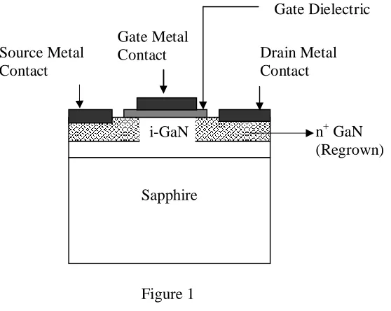
1.
The intended MOSFET Structure---129
2.
Tilted SEM image of regrown region for 30 minutes at 1040
oC with
precursor flow same as the base layer flows---130
3.
(a) Top view SEM image of regrown region for 20 minutes at 1060
oC with
precursor flow two-thirds of the base layer flows (b) Tilted view of the same
region as 3(a). The sidewall thickness is ~4
μ
m. Non-uniform coverage with
faceted islands.---131
4.
(a) Top view SEM image of regrown region for 5 minutes at 1000
oC with
precursor flow two-thirds of the base layer flows (b) Tilted image of the same
region as 4(a). Coverage of the regrown area is increased compared to the
growth at 1060
oC. No sidewall is seen in these 5 minutes of regrowth---132
5.
(a) Top view SEM image of regrown region for 10 minutes at 800
oC with
precursor flow two-thirds of the base layer flows. Complete coverage is
achieved (b) Tilted image of the same region as in 5(a). The GaN islands in
the field region and pits on the re-grown region are seen---133
4A1. SEM Images of the Regrown region at (a) 800
oC, (b) 1000
oC, (c)1060
oC.
Scale bar corresponds to10
μ
m---138
4A2. (a) Variation of island density (#/
μ
m
2) with temperature (b) Variation of
surface coverage with temperature---138
4A3. The Island growth occurring at topographical features---139
Semiconductor Structures
1.
AFM image of the Gate Oxide Surface---149
2.
HRTEM image of the interface between Ga
2O
3(Gd
2O
3) and GaN. Circled
regions denote individual nanocrystalline regions---149
3.
HRTEM image of the interface showing coherency between the oxide and the
underlying GaN---150
4.
I
d-V
dCharacteristics of GaN/InGaN/AlGaN HFET---151
6. Transmission Electron Microscopy Studies of Re-grown GaN Ohmic Contacts
on Patterned Substrates for MOSFET Applications
1.
(a) The bright field image of the transistor structure at the interface---163
(b) The Z-contrast image of the transistor structure at the interface---164
2. The bright field image of the re-grown GaN region. Inset shows the SADP of
the re-grown GaN region tilted to the standard [01-10] zone axis---165
3.
The high resolution image of the re-grown GaN and the Metal contact
interface---166
4.
EELS Spectrum of the Re-grown Region---167
5.
EELS Spectrum of the reaction layer at metal contact/n
+GaN interface. The
Ti and O edges are shown in the inset---168
6.
I
d-V
dCharacteristics that show the enhancement mode operation of the GaN
7.2
(a) Room temperature Raman spectrum of E
2mode and (b) A
1(LO) mode of
the intrinsic, gate and re-grown GaN---180
7.3
Curve fitting of LLP
+mode of the intrinsic and re-grown GaN. The broken
line is the measured spectral line after removing the E
g(2)peak of sapphire,
the solid line is the fitted curve---181
8. Device Results
8.1
Epitaxial design of AlGaN/InGaN heterostructure MOSFET device---190
8.2
DC Current-Voltage for AlGaN/InGaN heterostructure MOSFET with
L
g=1.5
μ
m gate length in depletion mode. Devices exhibited a corresponding
f
t= 8GHz (L
g·
f
t= 12GHz
·μ
m)---190
8.3
DC Characteristics of a long channel L
g=25 gate length FATFET structure
on InGaN/AlGaN MOSFET device which exhibits peak enhancement mode
transconductance of g
m=17.5 mS/mm for V
g= +5V---190
8.4
Capacitance
–
Voltage Profile for III-N heterojunction MOSFET structures
exhibiting two clear peak regions of operation---191
8.5
(a) I
d-V
dCharacteristics of the GaN MISFET with Si
xN
yas dielectric. The
Threshold Voltage is 5V and the gate voltage is increased in steps from
5-15V with 1 V step size (b) I
d-V
gCharacteristics of the GaN MISFET with
Si
xN
yas dielectric---192
9. Conclusions and Future Work
Chapter 1
Historical Background on GaN Metal Oxide Semiconductor
Field Effect Transistor (MOSFET)
Prologue to Thesis
The invention of the transistor in 1947 has revolutionized daily life. This
demonstration was the culmination of fundamental solid-state research over the preceding
decades. The first rectification action in a solid state material using a point contact based
on lead sulfide was achieved in 18741,2. However, it was not until 1947 the transistor
became a reality1,2. The motivation to have a working device at for highly integrated
audio communications triggered the research in point contact rectifying devices after the
World War II1,2. The unreliability, power inefficiency, and the size of the vacuum tube
hitherto was another reason motivating researchers to explore solid state materials and
point contact devices1,2,3. In addition, the detection of aeroplanes during and post World
War II necessitated the use of high frequency and short wavelength radar, mostly in the
MHz region1,2.
The need for high frequency, smaller, lower cost per function devices has been
the driving force behind semiconductor research for much of the past 60 years1,2. A
related thrust in semiconductor research is the change in conductivity achieved by doping
and carrier transport by applying electric field1. Initially germanium (Ge) was the
Ge, and Si could be used at higher junction temperatures compared to Ge, as well as
allowing for a wider range of doping1. The greatest motivator for the transition from Ge
to Si was the purity and quality of the Si/SiO2 interface which was essential for
MOSFETs fabrication1.
In the current dissertation work, GaN is an extension of this evolution due to its
advantageous physical properties, which enable the development of solid-state devices
for use in high power and high frequency devices. This research addresses the
development of GaN enhancement mode MOSFETs, a critical materials research step in
the realization of GaN integrated electronics.
1.1 Introduction
The development of electronic devices which operate at higher frequencies, higher
powers and higher temperatures has been a relentless pursuit through the history of
semiconductor technology. Rapid advances in device technology are most often based on
breakthroughs in semiconductor materials technology. This thesis explores such a
potential advance as a study of materials and structures enabling a new potential device:
The GaN MOSFET.
In the late 1950s, Si technology matured enough to fabricate planar and integrated
structures based on MOS field effect transistors (MOSFET) structures, and continuous
progress had been made in the production of transistors1-4. The devices have been scaled
to an extent where we have nearly two billion transistors on the latest micro-processor5.
The immediate implications we can think of with this astounding integration number is6:
1. The power density per chip has increased enormously,
3. The thickness of the gate oxide also becomes a few monolayers consistent with
the device lateral scaling.
Si may be an unideal choice at device local operating temperatures above 500K7. At
temperatures greater than 500K, the low bandgap of Si nullifies the effect of any external
dopant7. In addition to the bandgap, the other properties that are crucial to the state of the
art nanometer gate length structures, are the carrier drift velocity vd, and mobility e8-12.
The saturation velocity in a semiconductor is the maximum drift velocity of the
electron in the presence of an electric field, the limit being the thermal velocity7. At
electric fields above the value for saturation velocity, the energy imparted by the field is
transferred to the lattice rather than increasing the carrier velocity7. Therefore high
frequency current gain operation is limited for semiconductor devices with low saturation
velocity as the maximum speed of carrier transport is limited when they are transported
across a conducting channel7. The problem of electron carrier transport becomes
significant as the device scaling reaches a few nanometers where the applied voltage
between source and drain on the electron extends over a few nanometers and there is a
resulting high electric fields7-16,19-21. Another serious issue related to the low bandgap of
Si is the limit to high breakdown voltages relative to devices made of material with a
higher bandgap energy8-16,19-21. Therefore, it can be inferred that the solution to the
potential device scaling roadblocks is the choice of new material systems for MOSFET
channel structures that overcome the drawbacks of low saturation velocity, low
higher frequency and smaller device size1-3, the current trends also entail the use of wider
bandgap materials8-16,19-21.
The main properties of wideband gap materials that enable their use in high
power, high frequency, high temperature and high temperature applications are higher
mobility, higher saturation velocity, higher breakdown fields (Vb), lower dielectric
constant and higher thermal conductivity8-16,19-21. A commonly accepted road map of
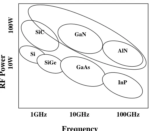
frequency of application versus the device power for different semiconductor material
systems is shown in Figure 18. This illustrates that the devices made of wide bandgap
materials like GaN and AlN encompass a wider range power and frequencies than
encumbent semiconductor materials. The wide bandgap materials are expected to be used
in making high power devices, high frequency operation, high temperature operation8-16,
and nano-scale devices17,18. The different values for each of these in comparison to Si is
listed in the table 1 and a combined figure of merit (CFOM) evaluated encompassing the
physical properties for Si, 6H-SiC, GaN and AlN is shown in figure 211-13,19-21.
It is quite evident from the figure that the CFOM of the wide bandgap materials is
an order of magnitude higher compared to Si11-13,19-21. The higher CFOM points to the
emergence of III-N based compound semiconductors for making of transistors for high
power and high frequency applications. Additionally for communication applications,
devices with high efficiency and good linearity are considered an essential requirement
for the next generation wireless technology thus supporting the realization of the dream
ubiquitous information technology (IT) society.8-15,19-21. Hence the need for wide bandgap
This materials research supports the development of advanced wireless and
information technology through the development of technologies for GaN enhancement
mode MOSFET structures. The growth of the material, the structural, optical and
electrical characterization, the device processing and the fabricated device results
References
1. W.F. Brinkman, D.E. Haggan, W.W. Troutman, IEEE Journal of Solid State Circuits,
32(12), pp1858-1865 (1997)
2. M. Riordan and L. Hoddeson, Crystal Fire, the Birth of the Information age, (New
York: Norton, 1997)
3. S.M. Sze, IEEE Proceedings, 69 (9), p1121 (1981)
4. J.A. Hoerni, IRE Trans. Electron Devices, p178 (1961).
5.
http://www.newsfactor.com/news/Intel-Surpasses-Billion-Transistor-Mark/story.xhtml?story_id=0020004ZUKHW (News Item Oct 19th,2005. Link posted
here on Nov 18th, 2005).
6. Nanoelectronics and information technology, Edited by Rainer Waser (Wiley-VCH,
Verlag GmbH & Co. KGaA, Second Edition, 2005), p 359-400.
7. Solid State Electronic Devices, Streetman and Banerjee (Sixth Edition, Prentice Hall,
New Jersey 2006), p96-97.
8. Y. Nanishi, IEEE Conference: The Fourth International workshop on Junction Technology, p 12-17 (2004).
9. M. Shur, R. Gaska, M.A. Khan, Materials Science Forum, 353-356, pp 807-814
(2001).
10. J. Hudgins, G.S. Simin, M.A. Khan, IEEE Conference Proceedings, p1747-1752
(2002).
11. S.J. Pearton, F. Ren. A.P. Zhang, and K.P. Lee, Materials Science and Engineering R
12. Notes of M.S. Shur from the
website:http://nina.ecse.rpi.edu/shur/advanced/Notes/16SiC.pdf (Nov 17th, 2005
8:00pm).
13. M.N. Yoder, IEEE Transactions on Electronic Devices, 43(10), pp1633-36 (1996).
14. T.P. Chow, R. Tyagi, IEEE Transactions on Electronic Devices, 41(8), pp1481-83
(1994)
15. R.W. Keyes, IEEE Transactions on Electronic Devices, 26 (4), pp 271-279 (1979).
16. K. Shenai, R.S. Scott, B.J. Baliga, IEEE proceedings, pp1811-1823 (1989).
17. C.M. Lieber, MRS Bulletin, p-486 (July 2003)
18. Y. Chui, Z. Zhong, D. Wang, W.U. Wang, C.M. Lieber, Nanoletters, 2 (2), p149-152
(2003).
19. R.W. Keyes, IEEE Proceedings Letters, pp 225 (1972).
20. B.J. Baliga, IEEE Electron Device Letters, 10 (10), pp 455-457 (1989).
Si
SiGe
GaAs
InP
SiC GaN
1GHz 10GHz 100GHz
1 0 0 W 1 0 W
Frequency
AlNR
F
P
o
w
er
Figure 1: The Power-Frequency Map: Illustrates the wide Power-Frequency range of GaN and AlN compared to other Semiconductors8.
Material Band-gap (eV)
Intrinsic Carrier Concentration (cm-3)
Relative
permittivity Mobility (cm2/Vs)
Break Down field
(106V/cm)
Vsat
(107cm/s) Thermal conductivity
(W/cmK)
Si 1.1 1.5x10¹⁰ 11.6 1350 0.3 1 1.5
GaAs 1.4 1.8x10⁶ 12.8 8500 0.4 2 0.5
GaN 3.4 1.9x10⁻¹⁰ 9 1200 3.3 2.5 2.1
4-H SiC 3.25 8.2x10⁻⁵ 10 720a)
650b) 2 2 4.5
6-H SiC 3 2.3x10⁻⁶ 9.7 370a)
50b) 2.4 2 4.5
AlN 6.2 9.4x10⁻³⁴ 9.1 300 1.2 1.9 1.7
InSb 0.17 2x10¹⁶ 16.8 77000 103 9.8 0.18
a)[11-20] direction
Table 1.1: Electronic Properties of various semiconductors8,12,13. AlN and GaN have superior saturation velocities and break down fields compared to other semiconductors.
0 50 100 150 200 250 300 350
Silicon GaN AlN 6H-SiC Electronic Combined Figure of Merit
CFOM vSEB
2
vSEB
2
Si
Figure 2: Combined Figure of merit11-13
GaN and AlN have a CFOM more than order of magnitude higher than Si.
Chapter 2
Background on Material and Device Technology
The theory of metal semiconductor contacts and the operation of metal oxide
semiconductor field effect transistors (MOSFET) will be discussed in this chapter. The
electronic properties of MOSFET structures are explored in detail, the applications
examined and the influence of the physical properties related to the choice of
alternative semiconductors is discussed. The properties of wide bandgap
semiconductor materials for the next generation electronics will thus be related to the
current research investigations. Material Science involved in the development of the
electronics technology will be described and the motivation for this research will be
explained. The main thrust of the research in this thesis is the development of highly
doped GaN ohmic contacts. Therefore, this chapter begins with a detailed description
of metal semiconductor contacts. The discussion considers both rectifying Schottky
contacts and ohmic contacts. The overview continues with a review of metal oxide
semiconductor (MOS) structures and the aspects of MOS structures which are relevant
to MOSFET devices.
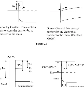
2.1 Metal semiconductor contacts:
The contact theory described below is taken from the standard
metal-semiconductor contact model listed in books either by Streetman or Sze1,2.
There are specifically two types of contact for metals directly on a semiconductor:
Schottky (or rectifying) and Ohmic contacts1,2. Ohmic contacts ideally allow
transport across a rectifying contact is asymmetric or non-linear. When a metal with
work function m is brought in contact with a semiconductor with work function s,
charge transfer occurs until the Fermi levels in both the semiconductors align to
establish thermodynamic equilibrium1,2. While the work function of the metal is a
fixed physical parameter, the work function of the semiconductor may be adjusted by
doping from degenerate n type ( s~ s) to degenerate p-type ( s~ s+Eg), where s is the
electron affinity measured as the energy difference between the vacuum level and the
semiconductor conduction band edge Ec, and Eg is the bandgap energy of the
semiconductor1,2. The alignment of Fermi levels is in accordance with the work
function differences between the semiconductor and the metal, and this defines the
characteristics of the contact as shown in figures 2.1 and 2.2.
2.1.1 Schottky Contacts:
When the m> s, the semiconductor Fermi level is initially higher than that of the
metal before contact is made1,2. To align the Fermi levels, the electrostatic potential of
the semiconductor must be raised (i.e., the electron energies must be lowered) relative
to that of the metal1,2. In an n-type semiconductor of Fig. 2.2(a), a depletion region is
formed near the junction1,2. The positive charge due to ionized donor ions within the
depletion region matches the negative charge in the metal1,2. The equilibrium contact
be decreased or increased by the application of either forward or reverse bias voltage.
When a forward bias voltage Vapp is applied to the Schottky barrier, the contact
potential is reduced from Vo to Vo-Vapp. As a result, electrons in the semiconductor
conduction band can move across the depletion region to the metal. This gives rise to a
forward current (metal to semiconductor) through the junction. Conversely, a reverse
bias increases the barrier to Vo + Vr and electron flow from the semiconductor to the
metal becomes negligible. In either case, flow of electrons from the metal to the
semiconductor is retarded by the barrier m- . The resulting diode equation is:
I = I0(eqVapp/ kT-1) --- (2.1)
Where is the ideality factor of the Schottky diode that varies from ~1-21-3.
Here the reverse saturation current Io is dependent upon the size of the barrier b
for electron injection from the metal into the semiconductor. This barrier is effectively
increased by the bias voltage. Thus a Schottky barrier diode is rectifying, with easy
current flow in the forward direction and little current in the reverse direction below
break down voltage1,2. In forward bias, the barrier is reduced and the electrons have
sufficient thermal energy to cross the reduced energy barrier1,2. In addition, if the
doping is high the band bending enables the electrons to tunnel through the barrier
similar to the thermionic electronic transport4. In GaN electronic devices Schottky
contacts are currently used as the gate structure for depletion mode heterojunction filed
effect transistor (HFET) devices.
An ohmic contact is the structure by which charge carriers may move from a
metallic material into a semiconductor material with the current density symmetric and
linear with applied electric field. From a device operation perspective, such contacts
should have minimal series resistance, have a linear relationship between current and
applied bias (obey Ohms law), and have no tendency to rectify signals1,2.
There are several mechanisms for electrons to move from the metal to the
semiconductor which are described in this section1,2. If
m< s, as seen in Fig. 2.2(b),
the Fermi levels are aligned at equilibrium by transferring electrons from the metal to
the semiconductor. This raises the semiconductor electron energies (lowers the
electrostatic potential) relative to the metal at equilibrium1,2. In the absence of any
fixed states which would fix the Fermi level energy at the interface, the barrier to
electron flow between the metal and semiconductor is small and easily overcome by a
small voltage1,2. This is termed the Bardeen model of ohmic transport behavior5.
Similarly, the case where m< s in a p type semiconductor would result in easy hole
flow across the junction1,2. No depletion region occurs in the semiconductor in these
cases since the electrostatic potential difference required aligning the Fermi levels at
equilibrium calls for accumulation of majority carriers in the semiconductor1,2.
An alternative model for ohmic contacts which often occurs in compound
at the metal-semiconductor contact as the resulting narrow depletion width promotes
efficient carrier transport.
There are four mechanisms for the transport of electrons between semiconductor
and a metal that are briefly described here from the models listed by Sze and
Morkoc2,4.
2.1.3 Electron Transport Mechanisms between a Semiconductor and Metal:
1.Thermionic Emission: For moderately doped semiconductors (Nd <= 1017cm-3), the
depletion region is relatively wide. Therefore, only electrons with sufficient thermal
energy surmount the barrier and transport across the interface as shown in figure
2.3(a)2,4. This results in a net current flow from the semiconductor to the metal2,4. The
mechanism is identical to the forward biased transport over Schottky barrier described
earlier.
2.Thermionic field Emission: For intermediately doped semiconductors (1017cm-3>
Nd < 1018cm-3), the carriers can gain a little energy by a combination of thermionic
emission and quantum mechanically tunnel through the barrier at higher thermal
energies due to the reduced depletion width as shown in figure 2.3(b)2,4.
3. Direct Tunneling (Field Emission): For heavily doped semiconductors (Nd
>1018cm-3), the depletion width is very narrow, and direct tunneling from the metal to
the semiconductor can occur at a high probability for electrons with no additional
thermal energy as shown in figure 2.3 (c)2,4. In the absence of a good metal to provide
an ohmic contact to the semiconductor through band alignment, which is the
interface states causes a fixed minimum potential barrier between the metal and
semiconductor, this is the approach adopted4. However, it is difficult to dope wide
bandgap semiconductors heavily and ohmic contacts to III-N semiconductors have
been fabricated by empirically developed multilayer structures coupled with rapid
thermal annealing to form a metallurgical junction with the minimum contact
resistance4.
4. Recombination in the Space Charge Region: Recombination of electrons and
holes in the space charge region (identical to the recombination processes in a p-n
junction)1,2, is another current transport mechanism that contributes to current flow
across a metal-semiconductor contact as illustrated in figure 2.3(d)2.
However, semiconductor surfaces often contain surface states due to incomplete
covalent bonds and other defects which can lead to charges at the metal-semiconductor
interface6. This could also be from a fixed charge from the native oxide which often
exists on semiconductors1,2,6. These interface states pin the Fermi level at a fixed
energy level regardless of the metal used to establish a contact as seen in figure
2.41,2,6,7.
The problem of Fermi level pinning due to the interface charge is one of the
historical drawbacks in wide bandgap compound semiconductor MOSFETs including
2.2 Metal Oxide Semiconductor Field Effect Transistor (MOSFET) and Device
Scaling:
The field effect transistor is a three terminal device with contacts referred to as a
gate, source, and a drain as shown in figure 2.51,2,12,13. In a MOSFET, charge is
transferred between source and drain contacts, with the ability to conduct between
source and drain modulated by the applied voltage to the gate. Thus the electric field
between the metal gate and the semiconducting A source-drain channel is the essential
functionality of the FET device. The metal-oxide-semiconductor gate stack above the
channel is the controlling structure for which a MOSFET is named. An important
property of these devices, in addition to signal amplification, is the possibility of
controlled switching from a conducting on-state to a non-conducting off-state
representing binary information, and, therefore a fundamental building block in digital
circuits1,2,12,13. An important advantage is the possibility of planar integration of many
MOSFET devices on a single chip1,2,12,13. Traditionally, MOSFETs have been
fabricated in Si because of the high quality and the thermodynamic stability of the
Si/SiO2 with a low density of interface states1,2,12,13,14. The development of MOSFETs
in other material systems such as GaAs although first unsuccessfully attempted in
196515, was explored only more recently due to the availability of epitaxially deposited
a gate dielectric with minimum interface density of states16-19. MOSFETs in GaN20-24,
and SiC/SiO225, have also been recently demonstrated. A detailed literature survey of
GaN MOSFET technology is listed in the next chapter. As a starting point, we will
materials system and gate scaling. As a result, the examination of Si MOSFET and its
limitations will help understand the emergence and the requirement of new materials in
MOSFET development.
In Si MOSFETs, source, drain, and channel structures are fabricated on single
crystal substrates1,2,13,14. The gate is traditionally made of polysilicon with a length (Lg)
as small as 50-100nm and a height of 50nm over an insulating dielectric above the
conductance channel structure. This poly-Si gate (M), insulating dielectric (O), and
semiconducting channel (S) is the MOS structure which forms the basis for Si
MOSFET operation. The central region of the transistor consisting of a lightly doped
or intrinsic silicon, the thin silicon dioxide layer and the silicided polysilicon contact,
form an MOS capacitor, which control the charge accumulation, depletion, or
inversion for the transistor. The figure 2.6 (a) shows a cross sectional view of a typical
Si MOSFET and its equivalent circuit in 2.6 (b) for electrical functionality26.
Equating physical properties of the MOSFET structure with equivalent circuit
forms the frame work of understanding the critical structure-property-performance
functional relationships in MOSFET materials research26. It can be noticed that there
are individual contact issues associated with the source, drain and gate which would
influence MOSFET operation. Ideally, source and drain contacts would be ohmic,
contact material systems for the next generation MOSFETs. Various silicides such as
TiSi2 have been introduced as contacts to source, drain, and gate contacts to lower the
device resistances. TiSi2 has excellent electrical conductivity at wire widths even
below 100nm13.
As satisfactory ohmic contacts have evolved for scaled MOSFETs, the continuous
downscaling of the device dimensions has resulted in the thickness of silicon dioxide
gate dielectric approaching the limit where tunneling causes excessive gate leakage
currents13,27-31. Gate leakage current leads to energy inefficiency in transferring
information as the difference between on-state and off-state MOSFET functioning for
low power digital logic applications. Hence, the recent trend has been to explore
alternative gate dielectrics with high permittivity yet compatible with Si technology.
The Capacitance of a typical MOS structure is given by
C = r oA/l --- 2.2
In the MOSFET analogy, ris the dielectric constant of the gate dielectric, A, the area
of the gate, and l, the thickness of the oxide13.
The device scaling requires that the total capacitance per unit area with the channel
to be high. Traditionally for scaled MOSFETs this was obtained by decreasing the
SiO2 thickness. However, very thin SiO2 is plagued by gate leakage due to tunneling13.
Therefore, an equivalent thickness of an alternative dielectric with a high dielectric
constant (K= r) will provide a higher physical oxide thickness than the SiO2, per unit
area while continuing to scale the equivalent oxide thickness13. This is the motivation
SiNx, HfSiOx, Al2O3, La2O3, Ta2O5, are under consideration and being explored for
silicon27-31. The International Technology Roadmap for Semiconductors (ITRS) in
2005 estimates that the dielectric constant of the gate dielectric needed for the 65nm
technology to be 6032
. TiO2 and Ta2O5 are predicted to be used for the 45nm
technology, while further scaling requires new ultra high K materials, potentially
strontium based dielectrics and perovskites32.
As seen in the figure 2.6, the source and drain regions are usually n+ or p+ doped
by a self aligned ion-implantation of dopants in a corresponding n-channel or
p-channel MOS structure respectively. The current from the source to drain is not
possible until a conductive channel is produced between them12,26,33. This is because
the band diagram of a MOSFET in equilibrium along the channel shows the Fermi
level flat and we notice that there is a potential barrier for an electron to go from the
source to the drain, corresponding to the built in potential of the lightly doped or
undoped channel source and drain12,26,33. This is illustrated clearly in the figure 2.7(a)
where the band diagrams of an n-p-n structure is shown with aligned Fermi
levels12,26,33. When a positive voltage is applied to the gate relative to the substrate,
positive charges are effectively accumulated on the gate metal through the removal of
free electrons in the metal in response to applied bias. In response, free negative
From the perspective of electric field potential, since electrons are electrostatically
induced in the p-type channel region, the channel becomes less p-type, and therefore
the valence band moves down, farther away from the Fermi level33. This effectively
inverts the channel from lightly doped p-type to n-type in the channel. This inversion
reduces the barrier for electrons between the source and drain through the channel. If
the barrier is reduced sufficiently by applying gate voltage in excess of the built in
barrier potential between source and drain, the threshold voltage (Vt) is achieved and
there is a significant current flow from the source to the drain as shown in figure
2.7(b)33. The threshold voltage of the MOSFET is the point where the conduction band
energy aligns with the Fermi level in terms of electrically applied bias at the gate33.
The MOS capacitors flat band diagram is shown in the figure 2.7(c). Flat band condition occurs when the metal gate and the semiconductor Fermi levels are aligned
without any applied voltage33.
A range of inversion, depletion, or accumulation in the semiconductor beneath an
MOS structure is best understood by consideration of the band structures at various
gate biases. Due to the large difference in electron affinity between Si and SiO2, the
potential barrier between the conduction band of the silicon and the silicon dioxide is
large and is a conduction band offset ( Ec) at the semiconductor-oxide interface33. The
energy band diagram of the MOS capacitors with both p-type and n-type
semiconductors are shown in figure 2.833. When a negative gate potential Vg <0 is
applied on the metal contact, the Fermi level of the metal increases and an electric field
the Si33. Because of the applied bias and the low carrier concentration, the Si bands
bend upwards at the SiO2 interface, leading to an accumulation of holes33. In order to
conserve charge, an equivalent number of electrons are accumulated at the metal side
of the MOS capacitor33. When a positive potential is applied at the metal contact, the
Fermi level moves down leading to the band bending in the silicon in the downward
direction. As a consequence, the hole concentration near the interface decreases and
this is called depletion. Charge neutrality requires the induction of an equivalent
amount of positive charge at the metal-oxide interface Qm in the semiconductor, as the
negative charge in the semiconductor Qs, explicitly, Qs=-Qm, with Qs=Qd where Qd
originates from the ionized donor states33. A further increase of the positive gate
potential, enhances the band bending such that at a certain gate potential the intrinsic
Fermi level crosses the Fermi level as shown in Figure 2.8 for case 2 where Vg>0.
Energetically it becomes now favorable for electrons to populate the newly created
surface accumulative channel33.
The surface behaves like an n-type semiconductor where the doping was created
by inverting the original p-type silicon with an applied field. This condition is called
weak inversion and the corresponding onset gate bias at the threshold voltage Vt33. The
negative charge at the semiconductor interface Qs consists of inversion charge Qi
inversion when the concentration of the electrons exceeds the hole concentration in the
substrate (Qi>Qd). The region near the semiconductor surface in this case has
conduction properties typical of n-type materials33. This electron conducting layer is
not formed by doping but by inversion of the originally p-type semiconductor due to
the applied voltage. This inverted layer, separated from the underlying p-type material
by a depletion region, is a key to traditional Si-MOS transistor operation33.
In the case of potential GaN MOSFETs, where there is wide bandgap energy
which would require inversion, enhancement mode operation is achieved by
accumulation of carriers in the channel. In the current work, the accumulation mode
devices having a conducting n-channel n+-i-n+ and n-i-n GaN structures were
investigated where i- represents the unintentionally doped GaN channel.
2.2.1 Modern trends in MOSFETs and scaling rules:
Scaling of MOSFETs to smaller dimensions is required to increase device density
and speed13. To maintain acceptable power dissipation per unit area, it is necessary to
simultaneously reduce total power consumption per device. One major change under
consideration when the gate length of the MOSFET is reduced to nano-scale
dimensions, corresponds to a reduction in channel structure dimensionality, such that
the corresponding electric field distribution in the channel region is increased from one
to two or three dimensions13. In traditional long channel MOSFET device structures,
the potential contours are nearly parallel to the oxide/silicon interface. The carriers in
the channel experience a largely one-dimensional field. For short channel devices in a
shown in Figure 2.933. Therefore, to maintain the transistor function for very small
dimensions numerous alternatives should be explored. Lack of saturation, gate oxide
degradation due to hot electrons, threshold voltage shifts, gate-induced drain leakage
and drain-induced barrier lowering (DIBL) are other problems with smaller MOSFET
dimensions13,33.
A common scaling approach for MOSFET devices is to reduce the device
dimensions in horizontal and vertical directions, as well as the voltage by the same
factor to maintain constant electric field conditions and hence electron transport
behavior at different device sizes13. Proportional increase in semiconductor doping
concentration is also needed to keep the electric field distribution in the semiconductor
unchanged13. The gate oxide thickness has to be decreased by the same factor to
maintain the oxide field, while decreasing the gate voltage13. This is necessary to
maintain the gate control of the channel and ensure good short channel behavior13. As a
result, the thinner the gate oxide, the greater are the two dimensional effects13.
Scaling rules are used to predict for future device dimensions and performance
parameters and link these projections back to material and structure requirements.
Ultimately, the use of thinner and thinner SiO2 gate oxide is limited by the gate leakage
as electron transport behavior through the gate dielectric changes from semi-classical
down the oxide has problems such as dielectric thickness variation, diffusion of
impurities like Boron from the gate that is highly doped, reliability and lifetime
problems, and as mentioned before the exponential increase in the gate leakage current
with decreasing thickness due to tunneling13. For example, the leakage current at a gate
bias of 1V changes from 1E-12 A/cm2 at 3.5nm to 10A/cm2 at 1.5nm13. The practical
SiO2 thickness limit in a MOSFET device is reached when the gate leakage becomes
equal to the off-state source to drain sub-threshold leakage current as well as
contributing to Joule heating per unit area in the off state13.
One attempt to improve oxide quality of the gate is the introduction of nitrogen
into SiO2. This leads to the formation of oxynitrides-SiOxNy. Nitrogen slows down the
thermal growth rate and improves the interface uniformity. Furthermore it reduces
boron penetration from the highly doped poly silicon gate stack and makes the oxide
less sensitive to hot electrons that may create defects in the dielectric and cause gate
leakage. Nitrogen is incorporated by growing the film in nitrous oxide or by having
post growth anneal in a nitrous oxide environment13.
2.2.2 MOSFET Substrate Advances:
The need for reducing parasitic capacitance to increase the speed of the circuits
and to obtain a fully depleted channel can be addressed by silicon on insulator
technology (SOI)13. In this technology devices are built in a thin silicon film on an
commercially produced by wafer bonding, etch back or ion-implantation13. Another
innovation being investigated is silicon on nothing (SON) where a region under the
gate is removed and possibly refilled with a dielectric material. A buried Si-Ge alloy
layer selectively under-etched in a mesa structure to realize the SON structure.
Although this is similar to SOI technology, this approach is potentially cost effective
compared to SOI technology13. A potential issue being addressed is the need to
dissipate heat through the substrate while simultaneously limiting substrate parasite
resistance and capacitance13. As such the identification and development of new
substrate materials is an active area of Si MOSFET research. Substrate integration
merits consideration as an issue in this semiconductor channel material research
project.
2.2.3. Reduced MOSFET Dimensions:
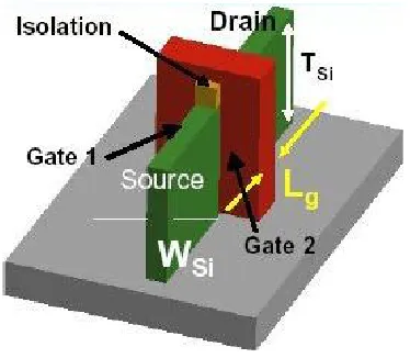
Transistors with double gates are investigated where two symmetric gates are
arranged in a planar or vertical configuration. A thin silicon ridge serves as the heart of
transistor with symmetric gates on both sides13,34-37. Current flow is confined to a
planar region of small effective thickness. An example of the FinFET is shown in
figure 2.1013,34-37. In such double gate systems, two symmetric gates produce two
inversion layers on both sides of the silicon layers. Transistor control is obtained
The scaling of the size and dimensions, the implementation of new materials and
the investigation of new transistor concepts are the present areas of focus in the
research and development of MOSFETs. However, scaling further and further
introduces quantum effects as active MOSFET structures are smaller than the
deBroglie wavelength for electrons in the material. As Si-MOSFET scaling technology
saturates, newer material systems that are consistent with the device scaling need to be
developed and explored.
2.3 Choice of New Materials for MOSFET Channel:
From the above fundamental explanations of the metal semiconductor contacts
and MOSFETs as well as the current device scaling trends, the possible outcomes are
that high field effects dominate the device performance as physical dimensions
approach the nanoscale. As channel lengths become less than 20nm, high electric
fields in the channel and source-drain tunneling of electrons through nano-scale
structures dominate MOSFET functionality38. To meet the high power density
requirements and minimize heating during the device operation, high thermal
conductivity, high saturation velocities and high breakdown voltages are necessary as
discussed in the previous chapter.
The two dominant breakdown mechanisms in high purity semiconductor materials
are Zener breakdown and avalanche breakdown39. In simple terms, Zener breakdown
is a bipolar breakdown which occurs when a junction is highly doped and the applied
reverse bias voltage is very high and an electron can tunnel directly from the
on either side of the p-n junction so much that the valence band on the p side lies
parallel to the conduction band on the n side as illustrated in figure 2.1139. Therefore,
there are empty states available for the electron from the valence band of the p side to
tunnel through to the conduction band on the n side and there will be an increase in the
current with increased reverse bias voltage. This free flow of carriers by tunneling
results in high currents and thus reverse bias break down39.
Avalanche breakdown is a unipolar breakdown which occurs instead in low doped
junctions where due to high applied electric field an electron in a transition region
collides with the lattice and generates an electron hole pair (EHP) in the transition
region38. This causes an increase in the drift current as the carriers created in the
transition region drift towards the n and p sides and during this drift they will trigger
further lattice collisions creating more and more EHPs that result in an increased drift
current39. This chain multiplication of carriers and the resulting high values of drift
currents result in high-currents across the material under high field conditions typical
for extreme high voltage, high power applications39.
From the above understanding of breakdown voltages, it is evident that increasing
the energy barrier to the generation of EHPs increases the breakdown voltage. For
defect free material, the energy required to create an EHP is the bandgap energy.
applications39. Moreover, the electric field that is applied increases the velocity of the
electron to a point beyond which the kinetic energy of the electron is given to the
lattice. This collision creates more EHPs. Therefore, it is evident that the saturation
velocity of the electron should be high as well as the field at which this velocity
saturates39.
2.4. Summary:
The considerations of carrier transport in devices and breakdown physics, strongly
motivates the investigation of the wide bandgap materials as an alternative channel
nano-material for MOSFET device structures. The properties of III-N materials offer a
potential solution to the next generation MOSFET electronics.
Once the decision to investigate alternative channel materials is made, new
research is necessary to investigate complimentary material and device issues required
for an alternative MOS channel material such as GaN. Specifically, for an efficient
device performance, there should be an off-state depleted channel which later becomes
conducting with an applied voltage, ohmic contacts to source and drain regions, as well
as minimum interface states between the semiconductor and the MOS gate stack. The
gate dielectric should also provide sufficient band offset ( Ec) to allow the MOSFET
operation as either p-MOS or n-MOS. It is in this purview of exploratory research into
which this GaN MOSFET development research falls. This opens new possibilities
and research directions for both semiconductor MOSFETs and the III-N scientific
communities. The goals of this thesis are directed towards demonstrating the potential
saturation and high saturation velocity for electrons and holes at high fields generated
by nanoscale dimensions.
2.5 Research Challenges:
The research challenges broadly fall into three categories, (1) GaN material
growth and characterization, (2) doping of GaN to obtain ohmic contacts and highly
doped source drain regions to supply the necessary free carriers to the channel in the
MOSFET and deplete the channel, (3) a suitable gate dielectric with minimum fixed
density of states (Dit) at the GaN/dielectric interface. These are the fundamental issues
that need to be addressed in consideration of GaN as an alternative MOSFET channel
material. The current status of the research for III-N materials, the possibilities, and
various techniques used to achieve the aforementioned objectives are explained in
detail in the chapter that follows with experiments focused on demonstrating the
References
1. Streetman and Banerjee, Solid State Electronic Devices (Sixth Edition, Prentice
Hall, New Jersey 2006), p221.
2. S.M Sze, Physics of Semiconductor Devices, (Second Edition, Wiley Eastern,
Mumbai, 1983) p 264.
3. S.P. Murarka, Metallization, Theory and Practise for VLSI and ULSI
(Buttersworth-Hienemann, Boston, 1993) p54.
4. H. Morkoc, Nitride Semiconductors and Devices (Springer 1999, New York),
p191.
5. J. Bardeen, Phys. Rev. 71, 717-727 (1947) 6. Cowley and Sze, J.Appl.Phys, 36, 3212(1965).
7. A. Zangwill, Physics at surfaces, (Cambridge University Press, New York, First
Edition, 1988), 55.
8. M. Hong, IEEE proceedings, p685(1998). 9. M. Passlack, Appl. Phys. Lett. 84, 2521(2004).
10. M. Hong, K.A. Anslem, J. Kwo, H.M. Ng, J.N. Baillargeon, A.R. Kortan, J.P,
Mannaerts, and A.Y. Cho, J.Vac. Sci. Tech B, (18) 3, 1453(2000)
11. M. Passlack, N. Medendorp, V.V. Afanasev, A. Stesmans, Appl. Phys. Lett. 85 (4), 597(2004).
12. Yannis Tsividis, Operation and Modeling of the MOS Transistor (Second Edition,
Oxfrod University Press, New York 1999) p91.
13. Nanoelectronics and information technology, Edited by Rainer Waser