Frequency Tunable Cedar-Shaped Antenna for WIFI and WIMAX
Mervat A. Madi1, *, Mohammed Al-Husseini2, and Karim Y. Kabalan1
Abstract—This article basically deals with the implementation of a negligible resistance varactor with a wide capacitance value into a modified version of a cedar shape antenna [1]. The electromagnetic characteristics of the antenna are manipulated both at the level of fractal geometry and electrical length using diodes. The antenna achieves tunability in a wide frequency range as a quad band antenna operating between 1.45 GHz and 4.6 GHz when 3 pairs of varactors are connected across slots. Pin diodes are also implemented leading to tunability in triple frequency bands between 3.7 GHz and 5.8 GHz. Moreover, implementing pin diodes as switches allows frequency reconfigurability of a dual band between 2.5 and 4 GHz and a single band of 6.6 GHz. The antenna RF frequencies have many applications in wireless communication that cover GPS, Bluetooth, WIFI, WIMAX, and WLAN.
1. INTRODUCTION
Frequency reconfigurable antennas afford more feasible, less complex and more compact multi-tasking systems in wireless communications necessary for accessing different RF bands on the same device. These include pre-filtering at the receiver, narrow band operation as well as wide band sensing in cognitive radio [2]. Different techniques were incorporated into microstrip antennas in order to manipulate their physical or electrical size [2, 3]. In addition to frequency reconfigurability, radiation pattern characteristics are maintained and high gain is achieved. In particular, as semiconductor devices such as pin diodes and varactors have attained minimal dissipation as well as mm sizes, they were easily mounted on microstrip antennas for RF applications [4].
Pin diodes are mainly used in switching ‘ON’ and ‘OFF’ and hence achieve frequency reconfigurability [5, 6]. However, varactor diodes have pn junctions with a depletion band subject to change in thickness under controlled reverse voltage up to 30 V, thus varying their capacitive load. Thereby adding varactors along the current path modifies the electrical length of the RF signal traveling through the antenna, resulting in frequency shift [7–9].
First, varactors were placed at the antenna radiating edges to increase frequency bandwidth [10, 11] by 30%. Then frequency tuning of microstrip antennas was obtained as a consequence of connecting varactors across slots [12]. Now, mounting varactors to existing designs adds new characteristics such as achieving a tunable filtenna from a wide band antenna [13], or beam scanning along with frequency tunability [14]. Moreover, frequency band notch tunability was also feasible by connecting a varactor across a slot introduced into an UWB antenna [15]. Note that the position of varactors on the antenna patch should be optimized for obtaining wide range of frequency tunability.
An antenna that can be adjusted to achieve either reconfigurability or tunability in the range frequencies for wireless communications is introduced in this paper. The antenna is a modified version of the cedar shape antenna previously introduced in [1].
Received 15 September 2017, Accepted 26 October 2017, Scheduled 17 January 2018
* Corresponding author: Mervat Akram Madi (mervatmadi@icloud.com).
Figure 1. HFSS model of the modified cedar shape antenna showing position of the coaxial feed from a top and lateral view.
Controlled DC input voltage is supplied through a power source to bias the varactors. Two RF chokes are used to connect the DC source terminals to the cedar top and bottom as shown in Fig. 2. The inductors are chosen with high inductance of 1µH to conduct the direct current and block the RF signal thus avoiding AC short.
The feed position maintains a triangular fractal shape of the design which exhibits through achieving multiple resonant frequencies when all slots are connected and frequency shifting when switches (pin diodes) are ON consecutively from top to bottom [17]. Moreover, pin diodes result in wide interval of frequency recongfigurabilty. Note that the fractal shape corresponds to a triangular shape which enlarges as the current flows from top to bottom.
In summary, the cedar shape of the antenna being meticulously designed in terms of dimensions is herein combining the fractal shape and efficiency of mounting diodes across the multiple slots. Pin diodes and varactors are usefully employed to achieve attractive applications that fall in WIFI, WIMAX, GPS, Bluetooth and WLAN bands.
2. PIN DIODE IMPLEMENTATION RESULTS
2.1. Comparison between Measurements and Simulations Results
(a) (b)
Figure 2. Fabricated models of the cedar shape antenna with (a) varactors and (b) pin diodes added across the three slots.
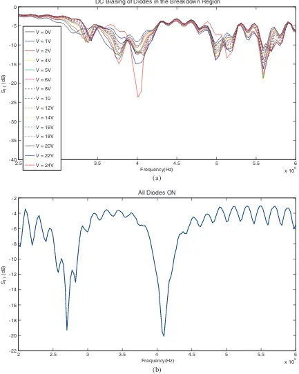
using a network analyzer to record the return loss (S11) variation with frequency, and a DC power
supply to bias the diodes. Fig. 3 shows the antenna measurements results of the return loss (S11) where
top subfigure corresponds to the case when all diodes are off and bottom subfigure corresponds to the case when all diodes are off and when all diodes are ON. First, a reverse voltage is applied across the antenna, so that all diodes function in the breakdown region with a variable capacitance in the range [0.7–1.3] pF as the voltage varies. Selected voltage values below 25 V are shown in Fig. 3(a) as no significant change is obtained at higher values. Consequently all the diodes are OFF, and the antenna is tunable in the frequency bands [5.59–5.8] GHz, [4.99–5.2] GHz, [3.77–4.1] GHz and shows weak resonance around 3.33 GHz as Fig. 3(a) shows. Simulations results are plotted in Fig. 4(d) and are very similar to the measurements. In fact, the tunability bands in simulations are [5.2–5.6] GHz, [4.74–5] GHz, and [3.85–4] GHz. Hence, a 0.2 GHz downward shift in frequency appears in upper bands in the simulations results.
When the diodes are biased with a forward voltage, they are all in the ON state. Fig. 3(b) shows the S11 plot over frequency in the range [2–6] GHz obtained from measurements done with all diodes
switched ‘ON’. The resonant frequencies are 2.7 GHz and 4.1 GHz. These results almost coincide with simulations as shown in Fig. 4(a) where resonance occurs at 2.45 GHz and 3.78 GHz.
Though during measurements, DC biasing is done over the three levels of diodes at a time, simulations show that while each pair is switched ‘ON’ from top to bottom, frequency shifts upwards between 2.45 and 7.1 GHz. Note that the interval of frequency is restricted to frequencies below 6 GHz in measurements as shown in Fig. 4(a). Also, simulations show that when bottom level diodes are OFF, lower frequency shifts from 2.45 to 3.1 GHz as shown in Fig. 4(b), while resonance around 4 GHz is maintained. However, when both bottom and second level diodes are off, frequency shifts to upper values (6.66 GHz) as shown in 4(c). Notice that the pin diode application achieves a triple band in most cases as shown in Fig. 4.
2.5 3 3.5 4 4.5 5 5.5 6 x 10⁹ -40
-35 -30
Frequency(Hz) V = 12V
V = 14V
V = 16V
V = 18V
V = 20V
V = 22V
V = 24V
2 2.5 3 3.5 4 4.5 5 5.5 6
x 109 -22
-20 -18 -16 -14 -12 -10 -8 -6 -4 -2
Frequency(Hz)
S11
(dB)
All Diodes ON
(a)
(b)
Figure 3. MeasuredS11 results for Coaxial fed antenna using pin diodes, (a) all Diodes are OFF, (b)
all Diodes are ON.
3. VARACTORS IMPLEMENTATION RESULTS
3.1. Measurements Results
1 1.5 2 2.5 3 3.5 4 4.5 5 5.5 6 -20 -18 -16 -14 -12 -10 -8 -6 -4 -2 0 Frequency(GHz) S11 (dB)
All diodes are ON
1 1.5 2 2.5 3 3.5 4 4.5 5 5.5 6
-14 -12 -10 -8 -6 -4 -2 0 Frequency(GHz) S11 (dB)
Diodes in seconfd and bottom levels are OFF
1 1.5 2 2.5 3 3.5 4 4.5 5 5.5 6
-18 -16 -14 -12 -10 -8 -6 -4 -2 0 Frequency(GHz) S11 (dB)
Diodes in bottom level are OFF
3 3.5 4 4.5 5 5.5 6
-16 -14 -12 -10 -8 -6 -4 -2 0 Frequency(GHz) S11 (dB)
All Diodes are OFF
C = 0.7pF C = 0.8pF C = 0.9pF C = 1pF
(a)
(b)
(c)
(d)
Figure 4. S11 simulated results for diodes: (a) all diodes are ‘ON’, (b) bottom diodes are ‘OFF’, (c)
bottom and second level diodes are ‘OFF’, (d) all diodes are ‘OFF’ with tunability obtained due to biasing. Capacitance range of each diode is [0.7–1.3] pF.
results are achieved over a wider range of frequency. While voltage is varied to bias 1SV325 varactors, the following results were obtained as shown in Fig. 5(a). At 25 V, resonance is obtained at 1.86, 3.33, and 4.3 GHz. As voltage is decreased, 4.3 GHz is tuned down to 3.93 GHz, 3.33 GHz is tuned down to 2.91 GHz, 1.86 GHz is tuned down to 1.6 GHz and a resonance at 2.54 GHz occurs when voltage is zero. Equivalently, since the capacitance is inversely proportional to the square root of the applied voltage [2], as capacitance increases, frequency shifts downwards. In brief the tunability bands in measurements of the 1SV325 are [1.6–1.86] GHz, [2.91–3.33] GHz, and [3.93–4.3] GHz, in addition to resonance at 2.54 GHz.
In fact each 1SV325 varactor capacitance changes between 7 pF and 80 pF when a reverse voltage between 0 V and 6 V is applied [19]. Therefore, a source voltage up to 25 V, exploited the full range of capacitance of all varactors.
On the other hand, a different varactor from SKYWORKS (SMV1211) has a similar size and hence could be mounted between the slots. Since it has a variable capacitance between 10 pF and 160 pF, slightly wider tunability bands are obtained for the same position of varactors. As Fig. 5(b) shows, highest resonant frequency of the antenna is tuned down from 4.4 to 3.94 GHz, middle band is tunable from 3.49 down to 2.93 GHz, and lower frequency is tunable from 1.91 to 1.35 GHz. Also, resonance at 2.44 GHz appears when zero volt is applied. Therefor the tunability bands for the SMV1211 varactor are [1.35–1.91] GHz, [2.93–3.49] GHz, and [3.94–4.4] GHz, in addition to resonance at 2.44 GHz.
3.2. Simulations Results
1 1.5 2 2.5 3 3.5 4 4.5 5 x 10⁹ -30
-25 -20
Frequency(Hz)
V = 11V V = 9V V = 7V V = 5V V = 3V V = 1V V = 0V
1 1.5 2 2.5 3 3.5 4 4.5 5
x 109 -35
-30 -25 -20 -15 -10 -5 0
Frequency(Hz)
S11
(dB)
SMV1211
V = 25V V = 23V V = 21V V = 19V V = 17V V = 15V V = 13V V = 11V V = 9V V = 7V V = 5V V = 3V V = 1V V = 0V (a)
(b)
Figure 5. MeasuredS11 results for Coaxial fed antenna using (a) varactors 1SV325 from Toshiba and
1 1.5 2 2.5 3 3.5 4 4.5 5 -45
-40 -35 -30 -25 -20 -15 -10 -5 0
Frequency(GHz)
S11
(dB)
1SV325 Varactor
1 1.5 2 2.5 3 3.5 4 4.5 5
-45 -40 -35 -30 -25 -20 -15 -10 -5 0
Frequency(GHz)
S11
(dB)
SMV1211 Varactor
(a)
(b)
Figure 6. Simulated S11 results for Coaxial fed antenna using varactors with a minimal resistance
bands, as 4 resonance bands appear. Moreover, resonant frequencies almost cover all applications that operate between 1.4 GHz and 4.6 GHz with the capability of tuning the antenna frequency. Therefore, the antenna shape along with implementation of varactors has yielded in attractive characteristics which serve multitasking in compact RF devices. In particular, the above obtained frequency bands, render the antenna functional in the RF bands of GPS, Bluetooth, WIFI, WIMAX, WLAN, and others. Further studies are required to investigate the gain of the antenna at the different operating frequencies.
4. CONCLUSION
The implementation of switches in RF antennas has shown successful results that are employed in miniaturizing electronic devices while achieving multitasking abilities. This paper aims at investigating the effect of using pin diodes and varactors in a fractal shape antenna with a cedar shape. Measurements confirm simulations results which show multiple resonance bands for both pin diodes and varactors. In particular, four bands corresponding to the four parts of the cedar appear when using varactors. These bands correspond to relatively low frequencies between 1.45 GHz and 4.6 GHz, which is the effect of using varactors with large capacitance range. In addition, pin diodes achieve reconfigurability when being switched OFF consecutively. Antenna resonant frequencies can be employed in various wireless applications such as GPS, Bluetooth, WIFI, WIMAX, and WLAN.
ACKNOWLEDGMENT
The authors would like to thank Mr. Salam Abiad and other AUB staff members in the ECE department for the technical assistance in fabricating the antenna.
REFERENCES
1. Madi, M. A., M. Al-Husseini, A. H. Ramadan, K. Y. Kabalan, and A. El-Hajj, “A reconfigurable cedar-shaped microstrip antenna for wireless applications,”Progress In Electromagnetics Research C, Vol. 25, 209–221, 2012.
2. Murugan, T. S. S. M., “A review on frequency reconfigurable microstrip antennas,” i-Manager’s Journal on Wireless Communication Networks, Vol. 4, 32–42, Jul.–Sep. 2015.
3. Zammit, J. A. and A. Muscat, “Tunable microstrip antenna using switchable patches,” 2008 Loughborough Antennas &Propagation Conference, 233–236, Mar. 2008.
4. Chen, J.-X., J. Shi, and Z.-H. Bao, “Tunable and switchable bandpass filters using slot-line resonators,”Progress In Electromagnetics Research, Vol. 111, 25–41, 2011.
5. Cao, Y. S. W. Cheung, and T. I. Yuk, “Frequency-reconfigurable multiple-input-multiple-output monopole antenna with wide-continuous tuning range,”IET Microwaves, Antennas&Propagation, Vol. 10, No. 12, 1322–1331, 2016.
7. Sato, S., S. Saito, and Y. Kimura, “A frequency tunable ring microstrip antenna fed by an L-probe with varactor diodes,” 2015 IEEE International Symposium on Antennas and Propagation USNC/URSI National Radio Science Meeting, 2409–2410, Jul. 2015.
8. Shynu, S. V., G. Augustin, C. K. Aanandan, P. Mohanan, and K. Vasudevan, “Development of a varactor-controlled dual-frequency reconfigurable microstrip antenna,” Microwave & Optical Technology Letters, Vol. 46, No. 4, 375–377, 2005.
9. Liang, J. and H. Y. D. Yang, “Varactor loaded tunable printed PIFA,”Progress In Electromagnetics Research B, Vol. 15, 113–131, 2009.
10. Al-Charchafchi, S. H. and M. Frances, “Electronically tunable microstrip patch antennas,” IEEE Antennas and Propagation Society International Symposium, 1998 Digest, Antennas: Gateways to the Global Network, held in conjunction with: USNC/URSI National Radio Science Meeting (Cat. No.98CH36), Vol. 1, 304–307, Jun. 1998.
11. Bhartia, P. and I. Bahl, “A frequency agile microstrip antenna,” 1982 Antennas and Propagation Society International Symposium, Vol. 20, 304–307, May 1982.
12. Babakhani, B. and S. K. Sharma, “Investigations on frequency agile microstrip patch antenna loaded with varactor diode,” 2013 IEEE Antennas and Propagation Society International Symposium (APSURSI), 664–665, Jul. 2013.
13. Atallah, H. A., A. B. Abdel-Rahman, K. Yoshitomi, and R. K. Pokharel, “Compact frequency reconfigurable filtennas using varactor loaded T-shaped and H-shaped resonators for cognitive radio applications,” IET Microwaves, Antennas and Propagation, Vol. 10, 991–1001, Jul. 2016.
14. Khidre, A., F. Yang, and A. Z. Elsherbeni, “Circularly polarized beam-scanning microstrip antenna using a reconfigurable parasitic patch of tunable electrical size,” IEEE Transactions on Antennas and Propagation, Vol. 63, 2858–2866, Jul. 2015.
15. Aghdam, S. A., “A novel uwb monopole antenna with tunable notched behavior using varactor diode,” IEEE Antennas and Wireless Propagation Letters, Vol. 13, 1243–1246, 2014.
16. Al-Husseini, M. M. M. and K. Y. Kabalan, “Effect of different varactor models on antenna tunability,” accepted at theHPCS Conf., Italy, Jul. 2017.
17. Petko, J. S. and D. H. Werner, “Miniature reconfigurable three-dimensional fractal tree antennas,” IEEE Transactions on Antennas and Propagation, Vol. 52, 1945–1956, Aug. 2004.
18. https://www.digikey.com/product-detail/en/skyworks-solutions-inc/SMP1322 079LF/863-1100-1-ND/2052232).