Beam Steering Antenna Array for 5G Telecommunication
Systems Applications
Mohamed H. Habaebi*, Mohanad Janat, and Islam Md. Rafiqul
Abstract—This work provides an in-depth study on a linear antenna array that consists of 32 elements of CRLH unit cells, and the main radiating beam can be controlled by changing the capacitance of the varicap diode that was designed and simulated with Advanced Design System (ADS 2014) software. ADS software was selected because of its flexibility in accommodating complex design equations. Results show that the main beam can be steered up to 50 degrees from the direction of maximum radiation by changing the capacitances. The main beam gain of the antenna array at boresight of 12 dB has been achieved with an impedance bandwidth of 3 GHz at 10 dB gain threshold. The antenna array performance was analysed in the mmWave frequency range at centre frequency of 28 GHz making it suitable for the upcoming 5G applications. The mmWave path losses were handled by increasing the gain of the antenna array and steering the main lobe over 50 degrees to balance the gain coverage tradeoff. The direction of the main beam is controlled by changing the varicap capacitance accordingly.
1. INTRODUCTION
In 2020 and beyond the LTE and its derivatives will be replaced with the more robust 5G, as a result of the massive and rapid increasing demands on mobile communications [1]. The upcoming 5G will provide higher capacity, less latency, higher bandwidth, and support mobility. The upcoming 5G will need 5 fundamental technologies to enable the upcoming generation which are small cells, full duplex, beamforming, MIMO and mmWave. The first technology is small cells that can be achieved by deploying macro cell to provide radio coverage or femtocell. Portable miniature base stations placed at every 250 meters which needs much less power to operate, in which service providers could install a huge number of these stations throughout the city to form a dense network that acts like a relay team. Moreover, 5G base stations will also have many more antennas than the base stations of today’s cellular networks to take advantage of another new technology like massive MIMO and beamforming. Second, the full-duplex technology will enhance the 5G reliability by allowing the 5G system to support all existing mobile phones with a half-duplex capability which will increase the 5G system overall performance. Finally, the Millimeter wave (mmWave) and terahertz systems are becoming, increasingly important in many scientific applications such as remote sensing, radio astronomy, plasma diagnostics, radar, and communication systems. In the last decade, a great deal of research was done on integrated antennas and many of the problems solved [2]. In recent years, the demand for highspeed cellular data has motivated the use of mm-wave carrier frequencies for future cellular networks. The design of future mm-wave mobile communication is highly influenced by the spatial multipath characteristics of the wireless channel. The mm-wave broadband provides practical values for designing cellular communication systems. The next generation will utilize mm-wave frequencies [3], in which it supports a very high bandwidth. However, the mm-wave frequency band suffers from high path losses [4]. The path loss issue can be resolved by utilizing very high gain antennas [3] in the communication system,
Received 18 September 2017, Accepted 2 December 2017, Scheduled 23 April 2018 * Corresponding author: Mohamed Hadi Habaebi (habaebi@iium.edu.my).
but the higher the antenna gain is, the lower the antenna viewing area will be, which makes the antenna a less sensitive transceiver. The antenna designers need to put more effort and focus on proper antenna design that can support the mm-waveband while balancing the antenna overall performance [6, 8]. For the upcoming 5th generation (5G), the antenna design will be an essential matter and must meet certain criteria such as small size and high performance, and specific materials are needed to support these high demands, which will make the metamaterials utilization inevitable due to the many aspects these artificial materials do pose like the negative permeability and permittivity [5]. The mm-wave antenna array in this paper utilizes metamaterials to improve the performance, by overcoming the shortcomings caused by operating in the of mm-wave band necessary for 5G, and shrink the antenna array size to make it suitable for smart phone applications.
A smart design should control the direction of the main radiating beam to the desired direction, which in return can assure high gain and maintain high coverage. In this paper, a 32 cascaded composite right/left-handed (CRLH) metamaterial unit cells antenna array is designed, in which the metamaterials are periodically printed on the FR4 substrate. These subwavelength metallic cells compose a uniform periodic structure, where this period defines the operating frequency, giving the substrate the high gain and large bandwidth needed for the mm-wave band in conjunction with the smaller footprint required for smart phone applications.
The following sections starting with theoretical analysis will handle the CRLH unit cell design and the requirements and followed by the installation of elements to antenna array body. Then a performance analysis is presented and finally, a conclusion of the work is presented.
2. MODELLING OF ANTENNA
Beamforming is a signal processing method used to control the direction of the main lobe of the radiated beam by controlling the value of the propagation constant to cause the desired phase shift between antenna array unit cells which is expressed as:
γ =α+J β (1)
whereα is attenuation constant, and β is the phase constant and can be expressed as:
β = 2π
λ (2)
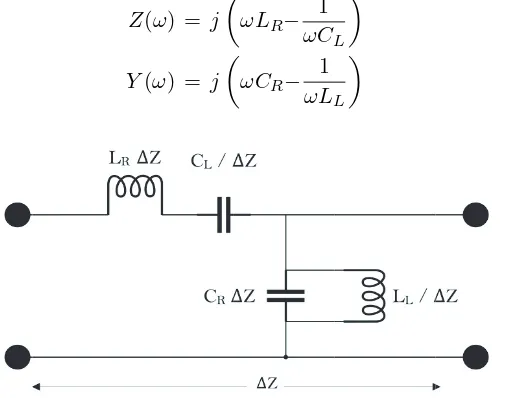
Figure 1 shows the equivalent circuit of composite right/left-handed unit cell metamaterial transmission line where inductance LR and shunt capacitance CL are both parallel to varicap diode CR and shunt
inductance LL. Impedance and admittance of transmission line can be expressed as:
Z(ω) = j
ωLR−
1
ωCL
(3)
Y(ω) = j
ωCR−
1
ωLL
(4)
For unbalanced line the dispersion relation can be expressed as [7]:
β(ω) =S(ω)
ω2L RCR+
1
ω2L LCL−
LR
LL
+CR
CL
(5)
From Equation (5) the radicand value will determine whether the band is a stop or passband. When it is positive, the phase constant is real, and it is a passband, and when the radicand value is negative, the nit will be a stopband. The most important property is when both the right hand and left hand are exhibiting the same contribution, at which the line is balanced, and it occurs when the shunt and series resonances [11] are expressed as:
LRCL=LLCR (6)
The propagation will split into two components, the right-hand phase constant and left-hand phase constant:
β(ω) =ωLRCR−
1
ω√LLCL
(7)
And the frequency is expressed as:
ω0 =
1 4 √
LRCLLLCR
(8)
The angle of the main lobe of the radiated beam is specified by:
θ= β(ω)
K0
(9)
whereK0 is the wave number in free space.
According to Equation (9), the angle of the main beam can be controlled by changing the frequency, which is not suitable for communication applications, or by changing the propagation constant to get the desired angle. The antenna array design in this paper is on a metamaterial substrate FR4 with dielectric constant εr = 4.35, according to Equations (7), (8), and (9), the values of the parameters
to be LR = 1.08 nH, LL = 0.538484 nH, and CL= 0.029 pF. The desired range of maximum radiation
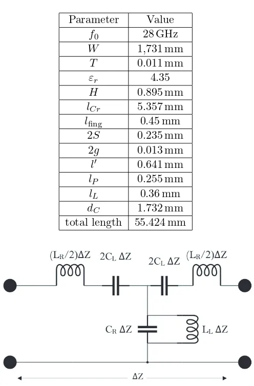
angle is 50 degrees by deploying Macomvaricap for abrupt tuning with capacitance changing, at the microwave frequency of 28 GHz, in the range of 0.033 pF to 0.06 pF. Microstrip line dimensions are thickness of 0.895 mm, widthW of 1.731 mm, and the body of the LW structure was selected equal to 55.424 mm, which corresponds to an ordinary microstrip line characteristic impedance of 50 Ohms. The array antenna parameters are summed up in Table 1. The in-depth design steps are illustrated in the following sections.
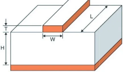
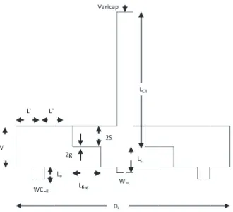
The array consists of 32 radiating cells, which are made with microstrip line technology. Figure 2 shows typical microstrip line dimensions, where L is the total length of the radiating element, W the width of the radiating element, T the thickness of the radiating element, and H the height of the substrate.
Table 1. Parameters of leaky wave antenna array.
Parameter Value
f0 28 GHz
W 1,731 mm
T 0.011 mm
εr 4.35
H 0.895 mm
lCr 5.357 mm
lfing 0.45 mm
2S 0.235 mm 2g 0.013 mm
l 0.641 mm
lP 0.255 mm
lL 0.36 mm
dC 1.732 mm
total length 55.424 mm
Figure 3. The equivalent symmetric circuit with microstrip elements and varicap.
The operating frequency is 28 GHz, and the cells were designed from Equation (1) in [10], whereεeff
is the effective dielectric constant and εr the relative dielectric constant. The characteristic impedance
Z0 can be calculated from Equation (4) in [10].
According to Equations (1) and (4) in [10], the effective dielectric constant εeff is 3.299, and the
characteristic impedanceZ0is 50 Ω. The cell uses a metamaterial substrate FR4 with dielectric constant
εrand height of 0.895 mm. The radiating element is copper with track thickness of 0.011 mm and track
width of 1.731 mm fed by a coaxial cable connected to surface mount adapter since the characteristic impedance is 50 Ω. The unit cell in Figure 1 can be equivalently described as a symmetric circuit as shown in Figure 3. The propagation constant between input and output terminals is expressed as:
A B C D
Vn+1
In+1
=e±γdc
Vn
In
(10)
3. DESIGN OF ANTENNA
3.1. Varicap Design CR and Capacitance CL
GaAs flip chip multiplier varicap, which is placed on MOVPE epitaxial wafers that can be utilized in the mmWave communications. These flip-chip diodes are fully passivated with silicon nitride and have protective coatings to prevent damage to the junction during automated or manual handling. The varicap is introduced to antenna body via a transmission line of length λg/2.
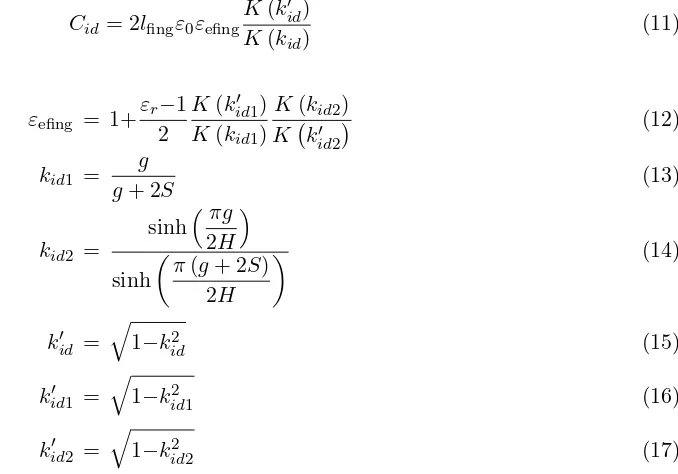
CL is an interdigital capacitor introduced to antenna body by two fingers as shown in Figure 4,
and the parameters needed for the interface are calculated from Equations (11) to (17) where Lfing is
0.45 mm; 2S is 0.235 mm; 2g is 0.013 mm.
Cid = 2lfingε0εefing
K(kid )
K(kid)
(11)
where:
εefing = 1+
εr−1
2
K(kid 1)
K(kid1)
K(kid2)
Kkid 2 (12)
kid1 =
g
g+ 2S (13)
kid2 =
sinh πg
2H
sinh
π(g+ 2S) 2H
(14)
kid =
1−k2
id (15)
kid1 =
1−k2id1 (16)
kid2 =
1−k2
id2 (17)
K (. . . ) factors are the elliptical integrals of the first kind, andLfing is the length of the fingers.
Figure 4. Ordinary configuration of an interdigital capacitor on the left, and to the right the realization of fingers designed for the interdigital capacitor for each antenna array unit cell.
3.2. Design of Inductance LR and LL
FirstLR/2 can be realized with a length of 3.05 cm which is much larger than the width of the microstrip
line used, e.g., 1.731 mm, resulting in 88.281 nH/m. To solve this problem, the LR/2 circuit shown in
(a) (b)
Figure 5. (a) The ordinary series inductance of each antenna array unit cell and (b) the equivalent circuit.
Figure 6. The equivalent T-circuit designed via microstrip.
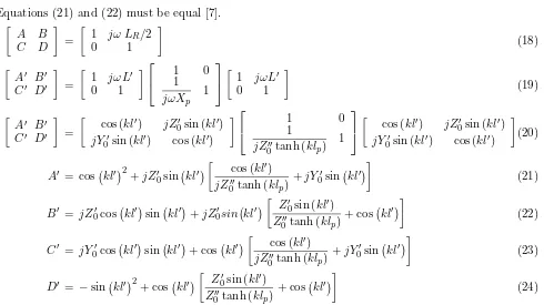
Equations (21) and (22) must be equal [7]. A B C D =
1 jω LR/2
0 1
(18)
A B C D
= 1 jωL 0 1 ⎡
⎣ 11 0
jωXp
1 ⎤
⎦ 1 jωL
0 1
(19)
A B C D
=
cos (kl) jZ0 sin (kl)
jY0sin (kl) cos (kl) ⎡
⎣ 11 0
jZ0tanh (klp)
1 ⎤
⎦ cos (kl) jZ0 sin (kl)
jY0sin (kl) cos (kl)
(20)
A = coskl 2+jZ0sinkl cos (kl
)
jZ0tanh (klp)
+jY0sinkl (21)
B = jZ0 coskl sinkl +jZ0sinkl Z
0sin (kl)
Z0tanh (klp)
+ coskl (22)
C = jY0coskl sinkl + coskl cos (kl
)
jZ0tanh (klp)
+jY0sinkl (23)
D = −sinkl 2+ coskl Z
0sin (kl)
Z0tanh (klp)
+ coskl (24)
According to Equations (20) to (24), parameterLR is 0.641 mm, andLP is 0.255 mm. Second, LL
is realized with microstrip line of length lL which is 0.36 mm. Figure 7 shows the microstrip structure
Figure 7. Leaky wave antenna array unit cell realized with microstrip structure.
Figure 8. First 4 elements of the Leaky Wave antenna array that has a 32 composite right/left-handed metamaterials unit cells with total length of 55.424 mm.
4. RESULTS AND ANALYSIS
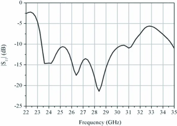
The antenna array resonates at the centered frequency of 28 GHz as depicted in Figure 9. The reflection coefficient is plotted against the frequency at port 1 where the first unit cell shows a promising performance, for as long as the antenna array elements are symmetrical, and the rest elements exhibit the same properties.
Figure 9. Reflection coefficient for a unit cell atCvar = 0.36 pF.
Figure 10. Total gain of the antenna array at the boresight.
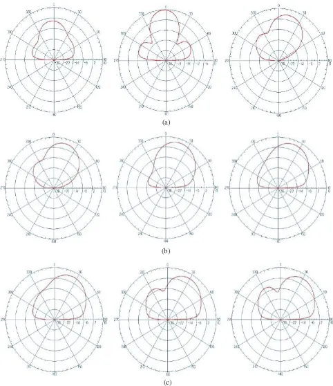
According to Figure 11, the main radiating beam can be controlled by changing the capacitance of the varicap diode. The antenna array in a range of 50 degrees can steer the main radiation beam in the direction where the signal is stronger. Table 2 shows the different varicap diode capacitances versus steering angles.
(a)
(b)
(c)
Figure 11. Realized gain patterns of the antenna array and the steering angle on the x-z planed for different varicap capacitances. (a)Cvar = 0.34 pF,Cvar = 0.36 pF,Cvar = 0.39 pF, (b)Cvar = 0.41 pF,
Table 2. Varicap diode capacitance vs steering angle.
Varicap Capacitance Steering Angle
0.34 pF 355θ
0.36 pF 0θ
0.39 pF 20θ
0.41 pF 25θ
0.44 pF 30θ
0.46 pF 35θ
0.49 pF 37θ
0.52 pF 40θ
0.56 pF 45θ
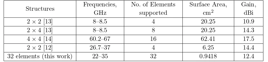
Table 3. Comparison of the presented array antenna with references.
Structures Frequencies, GHz
No. of Elements supported
Surface Area, cm2
Gain, dBi
2×2 [13] 8–8.5 4 20.25 10.9
2×4 [13] 8–8.5 8 20.25 14.3
4×4 [14] 60.2–67 16 62.41 17.5
2×2 [12] 26.7–37 4 6.25 14.4
32 elements (this work) 22–35 32 0.9418 12.4
5. CONCLUSION
In this work a linear antenna array that consists of 32 elements of CRLH unit cells and whose main radiating beam can be controlled by changing the capacitance of the varicap diode was designed and simulated. Results show that the main beam can be steered up to 50 degrees from the direction of maximum radiation by changing the capacitances. The main beam gain of the antenna array at boresight of 12 dB has been achieved with an impedance bandwidth of 3 GHz at 10 dB gain threshold. Performance of the antenna array was analysed in the mmWave frequency range at centre frequency of 28 GHz making it suitable for the upcoming 5G applications. The mmWave path losses were handled by increasing the gain of the antenna array and steering the main lobe over 50 degrees to balance the gain coverage tradeoff. The direction of the main beam is controlled by a Maccomvaricap, by changing the capacitance accordingly.
REFERENCES
1. Giust, F., L. Cominardi, and C. J. Bernardos, “Distributed mobility management for future 5G networks: Overview and analysis for existing approaches,”IEEE Communications Magazine, 142– 149, January 2015.
2. Dehos, C., J. L. Gonzalez, A. De Domenico, D. Ktenas, and L. Dussopt, “Millimeter-wave access and backhauling: The solution to the exponential data traffic increase in 5G mobile communications systems?,”IEEE Communications Magazine, 88–94, September 2014.
4. Elkhouly, M., C.-S. Choi, S. Glisic, C. Scheytt, and F. Ellinger, “Millimeter-wave beamforming circuits in SIGe BICMOS,” 2010 IEEE Bipolar/BiCMOS Circuits and Technology Meeting (BCTM), 129–132, Austin-Texas, USA, October 4–6, 2010.
5. Hur, S., T. Kim, D. J. Love, J. V. Krogmeier, T. A. Thomas, and A. Ghosh, “Millimeter wave beamforming for wireless backhaul and access in small cell networks,” IEEE Transactions on Communications, Vol. 61, No. 10, 4391–4403, October 2013.
6. Qiao, J., X. Shen, J. W. Mark, Q. Shen, Y. He, and L. Lei, “Enabling device-to-device communications in millimeter-wave 5G celluar networks,” IEEE Communications Magazine, 209– 214, January 2015.
7. Abdulla, M. A., “A dual mode CRLH TL metamaterial antenna,”Antennas&Propagation Society International Symposium, 793–794, IEEE, June 2014.
8. Song, J., S. G. Larew, D. J. Love, T. A. Thomas, and A. Ghosh, “Millimeter wave beamforming for multiuser dual-polarized MIMO systems,”2013 IEEE Global Conference on Signal and Information Processing, 719–722, December 3–5, 2013.
9. Kim, J. and A. F. Molisch, “Fast millimeter-wave beam training with receiver beamforming,”
Journal of Communications and Networks, Vol. 16, No. 5, 512–522, October 2014.
10. Ross, R. F. G. and M. J. Howes, “Simple formulas for microstrip lines,”Article Electronics Letters, Vol. 12, No. 16, 410–410, August 1976.
11. Wu, P.-C., L. Chen, and Y.-L. Luo, “Miniaturized wideband filtering antenna by employing CRLH-TL and simplified feeding structure,”Electronics Letters, Vol. 51, No. 7, 548–550, April 2015. 12. Djerafi, T., B. Youzkatli-el-Khatib, K. Wu, and S.-O. Tatu, “Substrate integrated waveguide
antenna subarray for broadband circularly polarised radiation,” IET Microw. Antennas Propag., Vol. 8, No. 14, 1179–1185, 2014.
13. Jung, E.-Y., J. W. Lee, T. K. Lee, and W.-K. Lee, “SIW-based array antennas with sequential feeding for X-band satellite communication,”IEEE Trans. Antennas Propag., Vol. 60, No. 8, 3632– 3639, 2012.