PARAMETRIC STUDY OF WAVEGUIDE SLOTS AND ANALYSIS OF RADIATION PATTERN FOR THE DESIGN OF WAVEGUIDE ARRAY ANTENNA
M. Mondal
Kalpana Chwala Space Technology Cell Department of E & ECE, IIT KGP Kharagpur-2, India
A. Chakrabarty
DEAN (Continuing Education) Electronics Electrical Communication Engg. IIT Kharagpur, India
Abstract—The characteristics of radiating longitudinal slots in a rectangular waveguide have been studied. A moment method solution is used with entire basis expansion and testing functions (Galerkin) including the effect of wall thickness. It is shown in this paper. 1) The determination of different parameters like VSWR, reflection coefficients and insertion loss are calculated with the results of normalize reactance and conductance. 2) The Taylor distribution approach with specific SLL for desired linear aperture array antenna. The resonant conductance or resistances are calculated from desired amplitude distribution. The formulation uses transmission matrix approach. The computed result shows excellent agreement with measured results. CST Microwave studio is used for the simulation and is totally based on FIT techniques.
1. INTRODUCTION
analysis as indicated by Elliott [1, 2] and Sangester and McCormick [3] Hamadallah [4]. Their works focus on small slotted array [8, 20], which includes the input impedance match and the aperture excitation distribution. The required computer cost and excessive computing time restrict their solution to small slotted array. Taking advantage of the results reported in the existing literature, the computation of impedance can be extended to that for a slot in a large array environment. It assumes that the radiated power is proportional to the slot active conductance. The array aperture distribution [9, 16] and input impedances [10, 15] depend upon the knowledge of these slot active admittance.
Waveguide slot array antennas have wide applications in radar and wireless communication systems because of their various advantages such as high power handling capability, low losses, and good control over side lobe levels (SLL). Desired array pattern is obtained controlling slot excitation, by adjusting the slot offset from the center line of the waveguide. Prior to the design of an array it is required to determine the resonant slot length, equivalent circuit and variation of the circuit parameters with the change in offset values. S-parameters of the slotted waveguide are computed for this purpose.
2. SYNTHESIS OF A LINEAR ARRAY ANTENNA
Design of a linear array antenna incorporating waveguide longitudinal slots as radiators is described. Prior to the design of an array it is required to determine the resonant slot length, equivalent circuit and variation of the circuit parameters with the change in offset value. S-parameters of the slotted waveguide are computed for this purpose. The resonant conductance or resistances resulting in the desired amplitude distribution are evaluated by using the similar recursive formulation developed.
The aperture distribution can be written as
A(v) =F(0) + 2 ∞
n=1
[F(nπ) cos(nπv)] (1)
wherev=z/L(zbeing the variable point on the aperture and length of the aperture is 2L).
The expression for the radiation pattern is
F(u) = ∞
n=1
F(nπ)sin(u−nπ)
and F(nπ) = 0 forn≥n. where
u = L
λ sinθ
L = length of the array
θ = angle measured from the direction of maximum radiation (n−1) is the number of equal side lobes. The power distribution across the linear aperture for 20 dB SLL andn= 3, normalized power distribution across the length is shown in Fig. 1.
Figure 1. Power distribution across the length of the aperture for SLL=20 dB andn= 3.
Figure 2. Transmission line model of an array of shunt radiators.
The voltage and current at the (N −1)th mode can be written as,
VN−1 IN−1
=
cosθd... . . jsinθd
jsinθd. . .cosθd
1. . .0
YN. . .1
VN
IN
(3)
Where VN−1 and IN−1 are the input side of the network, VN and IN are the output of the network (Nth section).
θd= 2π λg
d+π
λg being the guided wavelength of primary feed waveguide anddis the interelement spacing.
YN is the admittance of Nth radiator with respect to the characteristic impedance of the transmission line. Let the waveguide is matched terminated. If PN is the normalized power and ∆ is the fraction of power.
Dissipated at matched termination can be written that,
N
n=1
Pn+ ∆ = 1 (4)
For a system having normalized impedance equal to unity:
∆ =VN2 (5)
The conductance presented by theN-th radiation can be obtained
gn=
PN
V2
N = PN
∆ (6)
The transmission line model of an array ofN series radiators. The voltage and current at (N −1)th node can be written as,
VN−1 IN−1
=
cosθd... . . jsinθd
jsinθd. . .cosθd
1. . . ZN 0. . .1
VN
IN
(7)
ZN is the impedance of the Nth radiators normalized with characteristic impedance of transmission line.
The resistance of the radiator required for a particular aperture distribution can be determined by:
rN =
PN
I2
N = PN
∆ (8)
r0 and I0 are calculated using the values of gN ·r0/I0 gives the input reflection coefficients and 20 log10|(IN/I0)|gives the insertion loss. The voltage standing wave ratio is
VSWR = 1 +|R0/I0| 1− |R0/I0|
. (9)
Tilt of beam from the broadside direction
θ0 = si n−1
λ λg −
λ
2d
(10)
3. DETERMINATION OF SLOT PARAMETER
For a large array, the conductance’s presented by successive junctions are negligibly small, the reflection from the individual junctions can be neglected for the evaluation of desired conductance values. The values ofIN and gN, using the transmission matrix for Nth junction calculation. Calculate the values of this design of slot conductance assumes all the slots to be at resonance, for that particular case the inter element spacing is equal toλg/2. The required shunt conductance to obtain the desired amplitude distribution for given power dissipation in a match terminated load and for given inter element spacing. The expression for the slot conductance with power can be written in close form and is given by
gn=
Pn N m=1
Pm
(1−∆)
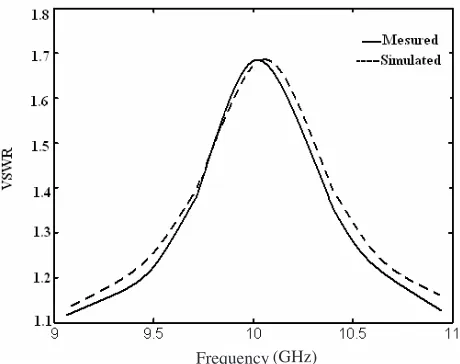
The conductance satisfying the desired amplitude distribution for inter element spacing equal to λg/2. Fraction of power (∆) are varies from 0.1 to 0.2. R0 andI0 are calculated using the value ofgn. The voltage standing wave ratio (VSWR) is given by
VSWR = 1 +|R0/I0| 1− |R0/I0|
(12)
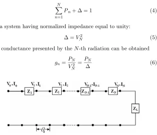
Using the above relation variation of VSWR, insertions loss and input reflection coefficients with frequency are evaluated for frequency range between 9 GHz to 11 GHz.
Frequency (GHz)
Figure 4. Measured (solid line) and simulated (dashed line) for VSWR calculation of the array.
4. DESIGN OF A LINEAR ARRAY ANTENNA
(dB)
Figure 5. Variation of insertion loss with frequency.
Figure 6. Linear array antennas.
termination of the primary guide and the fraction of incident of power absorbed in the terminating load. The mathematical relation for the evaluation of conductance contain the inter element spacing as a parameter in the recursive relation. The array is symmetric with respect to the central element and offsets of the first, second, third and fourth elements are 3, 4, 5, 6 and 7 mm respectively. Length and width of each slot are 14.5 and 2 mm respectively. Here, the slot lengths are taken identical due to our limited fabrication facility. Inter element spacing is taken as 25 mm for proper input impedance matching.
The waveguide array antenna is shown in Fig. 6.
design frequency are −21 and −7.9 dB respectively. Measured beam tilt angle towards the matched termination is 13◦. SLL is−14.8 dB.
It is seen that the strength of the slot aperture electric field increases with the increase of displacement from the waveguide center line. The measured results are quite similar with simulated results.
Figure 7. Measured (solid line) and simulated (dashed line) for S
parameter calculations.
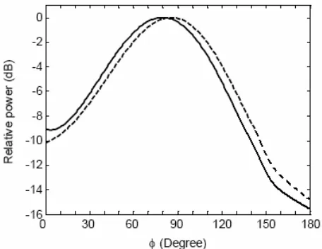
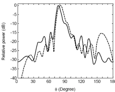
Figure 9. Measured (solid line) and simulated (dashed line) for H -plane calculation of the array at 10 GHz.
5. CONCLUSION
In this paper, a linear array antenna of waveguide longitudinal slots and its experimental results are presented. The procedure to design a linear array antenna with a specified SLL is described. Taylor distribution for a linear aperture has been adopted to obtain the required SLL. Required resonant conductance or resistances to achieve the desired aperture distribution are determined by considering a transmission line model of the array. The simulated radiation patterns of an isolated longitudinal slot show that the diffraction effects from the edges of finite size ground plane only affects theE-plane radiation patterns of the slot.
REFERENCES
1. Elliott, R. S. and L. A. Kurtz, “The design of small arrays,”IEEE Trans. Antennas Propagation, Vol. 26, 214–219, Mar. 1978. 2. Elliott, R. S., “Improved design procedure for small arrays of shunt
slots,” IEEE Trans. Antennas Propagation, Vol. 31, 48–53, Jan. 1983.
4. Hamadallah, M., “Frequency limitations on broad-band perfor-mance of shunt slot arrays,” IEEE Trans. Antennas Propagtion, Vol. 37, 817–823, July 1989.
5. Taylor, T. T., “Design of line source antenna for narrow beam width and low side lobes,”IRE Trans. Antennas Propag., Vol. 3, 16–28, Jan. 1955.
6. Yevstropov, G. A. and Tsarapkin, “Investigation of slotted waveguide antennas with identical resonant radiators,” Radio Engg. Elect. Phys., Vol. 10, No. 9, 1429, Sep. 1965.
7. Raju, G. S. N., “Investigations on slot coupled junctions and radiating slots,” Ph.D. dissertation, Indian Institute of Technology, Kharagpur, Dept. Electron. and Elect. Eng., India, 1987.
8. Paramesha and A. Chakrabarty, “Waveguide as a near-field measuring probe of the two-element array radiator,” Progress In Electromagnetics Research B, Vol. 7, 245–255, 2008.
9. Das, S. and A. Chakrabarty, “A novel modeling technique to solve a class of rectangular waveguide based circuit and radiator,”
Progress In Electromagnetics Research, PIER 61, 231–252, 2006. 10. Tiwari, A. K., D. R. Poddar, and B. N. Das, “On the equivalent
radius of a radiating slot in impedance calculation,” Progress In Electromagnetics Research, PIER 74, 47–56, 2007.
11. Khalaj-Amirhosseini, M., “Analysis of longitudinally inhomoge-neous waveguides using the method of moments,” Progress In Electromagnetics Research, PIER 74, 57–67, 2007.
12. Das, S., A. Chakrabarty, and A. Chakraborty, “Characteristics of an offset longitudinal/transverse slot coupled crossed waveguide junction using multiple cavity modeling technique considering the TE00 mode at the slot aperture,” Progress In Electromagnetics Research, PIER 67, 297–316, 2007.
13. Park, J. K., J. N. Lee, D. H. Shin, and H. J. Eom, “A full-wave analysis of a coaxial full-waveguide slot bridge using the Fourier transform technique,” Journal of Electromagnetic Waves and Applications, Vol. 20, No. 2, 143–158, 2006.
14. Khalaj-Amirhosseini, M., “Analysis of longitudinally inhomoge-neous waveguides using the Fourier series expansion,”Journal of Electromagnetic Waves and Applications, Vol. 20, No. 10, 1299– 1310, 2006.
Letters, Vol. 3, 187–195, 2008.
16. Lim, K. S., V. C. Koo, and T. S. Lim, “Design, simulation and measurement of a post slot waveguide antenna,” J. of Electromagn. Waves and Appl., Vol. 21, No. 12, 1589–1603, 2007. 17. Eldek, A. A., A. Z. Elsherbeni, and C. E. Smith, “Rectangular slot antenna with patch stub for ultra wideband applications and phased array systems,” Progress In Electromagnetics Research, PIER 53, 227–237, 2005.
18. Zhang, M. and Z. Wu, “The application of MoM and EECS on EM scattering from slot antennas,”Progress In Electromagnetics Research, PIER 21, 307–318, 1999.
19. Li, B., R.-Y. Zhu, L. Liang, and C. H. Liang, “Study on high gain waveguide array antenna with SRR structure,” Journal of Electromagnetic Waves and Applications, Vol. 21, No. 5, 615–627, 2007.