General Robotics Corporation
TBC USER MANUAL
740-1006-FO
Revision Table
DATE DESCRIPTION
NOV 80 ADD DC-DC CONVERTER SEP 81 ADDS ALL Q-BUS FINGERS FEB 82 TERMINATE BITS 18-21 MAR 82 CORRECTIONS
OCT 82 IMPROVE DC-DC CIROrIT
MAR 83 POWER SENSE=359MS, DROPOUT TO 1 1/2 CYCLES OCT 83 UPDATE
AUG 84 REVISION JAN 85 UPDATE
NOTE: Date indicates current level of manual revision.
1.
2.
3.
General Description • • • • •
· . . .
. .
. . .
1.1 Introduction • • • • • • •1.2 Purpose and Use • • • • • • 1.3 Description • • • • • • • •
· . . . .
.
. . .
· .
-.
. . .
·
.
. .
.
.
.
. .
· . .
· . . .
·
.
.
.
. . .
. .
.
.
1.3.1 Physical Description •1.3.2 Electrical Description
· . . .
.
. . .
. .
. . . .
1.3.3 Performance • • • • • • •·
.
.
. .
. .
.
. . .
.
. .
.
Figure 1 - Block Diagram •· .
••
.
• •.
·
• • •.
·
• • • • • • •. . . .
. .
Operation • • • •2.1 Introduction. • • • •
•
• • • • • • • • ••
• • • • • • • • • • • ••
• • • • • • • • • ••
·
.
2.22.3
Operating Requirements • • • • • • • • • • • • • Signal Definitions • • • • • • • • • • •
Table 2.1 Signals Between TBC and Qbus • • • • Table 2.2 Jl Signal Definitions • • • • •
Table 2.3 J2 Signal Definitions • • • • • • • • Installation and Checkout. • • • • • • • • • •
• • • • • • • • • • • • •
·
.
•·
. .
• • • • • • • •·
.
•·
. . .
3.1 3.2Introduction • • • • • • • • •
Unpacking and Visual Inspection
·
.
• • • • •·
.
• • 3.3 Installation • • • • • • ••
• • • •·
. .
• • • • • •3.3.1 Console Panel and Cable • • •
·
.
• • • • • Figure 3-1 TBC Switch & Cable Assy • • • •3.3.2 Console-Related Options. • • • • • • 3.3.2.1 Line Time Clock • • • • • •
Figure 3-2 Ehable LTC option • • • Figure 3-3 External LTC option • • • 3.3.2.2" LED and Lamp Options. • • • • •
Figure 3-4 LEn and Lamp options • • • • 3.3.2.3 Boot Option • • • • • • • • 3.3.3 AC Power • • • • • • • • • • • • • • •
Figure 3-5 AC Transformer. •
Figure 3-6 Power Signal Generation Timing • 3.3.4 PROMS. • • • • • • • •
3.3.5 3.3.6
Table 3.1 Table 3.2 Table 3.3 Table 3.4
Power Options • • • • • • • • • PROM Starting Address • • • • • PROM Window Size. • • • • PROM Address Range • • • • • • Software Registers •
Backplane Position •
·
• •.
• • • •·
. . .
•
•.
. ·
•·
.
.
TBCII User's Manual
1. GENERAL DESCRIPTION 1.1 Introduction
The TBC (Terminator/Bootstrap/Clock) module is a dual-height, LSI-JI*, QBUS* compatible module. The TBC contains most of the support functions required when integrating an LSI-II computer system. The TBC was de-signed to operate in a General Robotics backplane confi~uration, as well as other backplanes capable of accepting LSI-II QBUS compatible modules.
1.2 Purpose and Use
The last module in a QBUS backplane must be a terminator which provides a 220 Ohm impedance for the QBUS. The TBC provides termination for 22 ad-dress bits and various other lines as required by DEC* specifications. The processor module requires power sequencing signals in order to initialize itself and other modules when the power is turned on. The TBC provides BPOK and BDCOK signals for proper power-up sequencin~. The TBC module also has a power status LED and optional cable connections to pro-vide remote power status indication.
Space is provided for two 8-bit EPROMS or PROMS to be used for a bootstrap. Their addressing is set to respond to 773000(8) with a window size of 256(10) words. The window size may be changeo to 512,1024, or 2048 words and the address may be placed at any multiple of the window size in the I/O page by modifying a set of jumpers on the board. EPROMS of the 2704/2708/2716 family or equivalent may be used. General Robotics offers several standard EPROM sets which bootstrap multiple devices in-cluding RX02, RK05, RP02, RL02, many 8" and 5 1/4" winchester disk subsystems, SMD disk subsystems, and non-standard high density floppy disk subsystems. Custom EPROM sets are available on special request at additional charge. Options also provide for changes in the F.PROM start-ing address and the window size in the memory map.
The TBC provides for an optional remote console panel which includes a processor RUN status indicator, RUN ENABLE/HALT switch, and options for a Line Time Clock (LTC) switch, a Bootstrap switch, and a DC power status indicator. The standard option provided by GRC includes a 15" cable as-sembly with a switch bracket containing the RUN F.NABLE/HALT switch and an integral RUN indicator lamp. The cable has sufficient wires to allow all console options.
The TBC has a Line Time Clock (LTC) which, when activated, generates an interrupt on the BEVENT line of the CPU. The LTC is turned on by soft-ware when using RTll V3.0 or later. Options provide for an external clock input, an external clock enable, and interrupt line (~IRO L) rather than event line (BEVENT L) stimulation. Line time clock signals come from an external 24 VAC center-tapped transformer linked to the 50 or 60 Hertz AC power.
1.3 Description
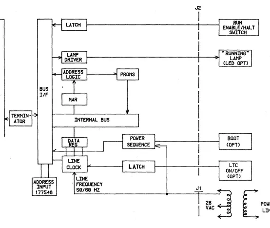
This section contains a general description of the physical, electrical, and performance specifications of the TBC. For more detailed infor-mation, refer to sections 2, the Block Diagram in Fig. 1, and the layout diagram Fig. 3.7 • •
1.3.1 PhYSical Description
The TBC comforms to standards for LSI-II compatihle modules, based on Digital Equipment Corporation standards for dual height modules.
The TBC is a dual height module designed to fit in a ~eneral Robotics, DEC, or any other LSI-II QBUS compatible backplane. The module is a two layer, computer grade, printed circuit board conforming to the hi~hest
standards of quality control. The module has one 3 pin connector for re-ceiving 24 VAC from an external source for the Line Time Clock (JI). It also has a 2xS pin connector (J2) to provide external controls and indi-cators, such as a Line Time Clock, a RUN ENABLE/HALT switch, and the RUN indicator lamp. A DC Power OK LED is installed near the front ed~e of the module adjacent to J1 (24 VAC) and J2 (console cable).
1.3.2 Electrical Description
The TBC conforms to specifications for LSI-II compatible modules. Con-nections provided to interface the module to the OBUS are LSI-II compatible. Connections for remote console functions are provided by a 10 pin header J2. Power line signals for the power sequencing circuits and the Line Time Clock are provided through the 3 pin connector JI. See section 3 for a detailed description of the OBIJS and auxiliary signals.
1.3.3 Performance
cr
TERMIN-~
ATOR
KLATCH
J
LLAMP
1
DRIVER
J
~ADDRESS
l
LOGIC
J
1.
PROMS
J
~
BUS
.
I/f
J
MAR
'V
~
INTERNAL BUS
J
1
l
~1A
J
.t!. ..1 ~ ~ .1 .1 1
l
H
LINE
L
CLOCK
L
'I
'LINE
ADDRESS
. FREOUENCY
INPUT
50160 HZ177546
r'
POWER
SE~UENCE
1'E---l
{ LATCH
J
l
'1 Block Diagram Figure
-TBCli User's Manual
J2
I
RUN
I
ENABLE/HALT
SWITCH
I
.. RUNNING"
J
~LAMP
I
-
(LED OPT)
I
I
I
I
I
1
BOOT
I
(OPT)
I
LTC
ON/OfF
I
(OPT>
Jt
-I
26
[
2. OPERATION 2.1 Introduction
This section describes the specific environmental and power requirements for the TBC module. Included are definitions of the QBnS and auxiliary signals.
2.2 Operating Requirements 2.2.1 Environmental
The following temperature and humidity specifications should be adhered to in order to ensure proper operation of the TBC module.
Storage Temperature
5 to 65 degrees C (41 to 149 degrees F) Operating Temperature
5 to 60 degrees C (41 to 140 degrees F) Humidity
10 to 95 % (non-condensing)
Air flow should be maintained across the module to ensure maximum tem-perature rise across the board of 5 degrees C (9 degrees F).
2.2.2 Power
Power required by the TBC module as measured at the backplane connection is as follows:
+5 VDC + 5% at 1.0 Amp +12 VDC
+
3% at 0.1 AmpTBCII User's Manual
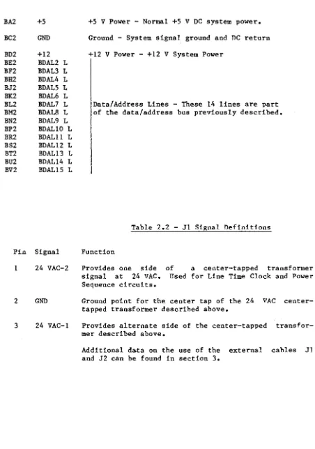
2.3 Signal Definitions
Table 2.1 defines the signals between the TBC module and the OBUS. Table 2.2 defines signals on Jl. Table 2.3 defines the signals on connector
J2. BUS PIN AAI ABI ACI ADI AFI ARI AJI AMI ANI API
Table 2.1 - Signals Between TBCn and QBTTS
MNEMONIC BIRQ5L BIRQ6L BDALI6 BDALI7 SSPARE2 SRUNL GND GND
BDMR L BHALT L
DESCRIPTION Not Used Not Used Not Used Not Used
Special Spare (SRUNL KDFI1-AA L~I-ll/73). This pin is tied to AHI on 11/02 and 11/23 CPU modules. Backplane pins AFI and AHI must be tied together on the backplane when using a 11/73
cpu.
This should be done on slot one only.This signal is asserted when the processor is in a run state. It is used by the THC to drive the run light. This pin is a special spare and is not bussed on the DEC backplanes, but is bussed on GRC's backplane. Used by LSI-l1/02 and LSI-ll/23. Pin ARI tied to AFI on these modules.
Ground - System signal ground and DC return. Ground - System signal ground and DC return. Not Used
Processor Halt - When BHAtT L is asserted, the proce-sor responds by halting normal program execution. External interrukpts are ignored, but memory re-fresh interrupts (enabled if W4 on the processor module, KDII-F only, is removed) and DMA
request/grant sequences are enabled. When in the halt state, the procesor executes the ODT microcode and the console device operation is invoked.
--CAUTION--The user must avoid multiple DMA delay refresh transfers (burst or ation. Complete refresh cycles every 1.6 ms if required.
ATI GND BAI BDCOK H
BBI BPOK H
BCI DALl8L BDI DAL19L BEl DAL20L BFI DAL2lL BJI GND BKI EXT CLK BMI GND BNI BSACK L BPI BIRQ7L BR1 BEVNT L
BTl GND BVI +5
AA2 +5 AC2 GND
AD2 +12 AE2 BDOUT L
Ground - System signal ground and DC return.
DC Power OK - TBC generated signal that is asserted when there Is sufficient DC voltage available to
sustain reliable system operation.
Power OK - Asserted by the TBC when primary power is normal. When negated during processor operation, a power-fail trap sequence is initiated.
Not Used Not Used Not Used Not Used
Ground - System signal ground and DC return
Ground - System signal ground and DC return Not Used
Not Used
External Event Interrupt Request - When asserted, the processor responds (if PS Bit 7 is 0) by entering a service routine via vector address 100. A typical use of this signal is a line time clock interrupt. The 11/23 processor arbitrates as a level 6 inter-rupt.
Ground - System signal ground and DC return +5 V Power - Normal +5 V DC system power +5 V Power - Normal +5 V DC system power Ground - System signal ground and DC return +12 V Power - +12 V DC system power
AF2 BRPLY L
AH2 BDIN L
AJ2 BSYNC L
AK2 BWTBT L
AL2 BIRQ4L
AM2 BIAKI L
AN2 BIAKO L
TBC11 User's Manual
Reply - BRPLY L is asserted in response to RDIN L or BDOUT L and during IAK transactions. It is ~ener
ated by a slave device to indicate that it has placed its data on the RDAL hus or that it has ac-cepted outupt data from the bus.
Data Input - BDIN L is used for two types of bus operation:
1. When asserted during BSYNC L time, RDIN L im-plies an input transfer with respect to the current bus master, and it requires a response (RRPLY L). BDIN L is asserted when the master device is ready to accept data from a slave device.
2. When asserted without BSYNC L, it indicates that an interrupt operation is occurring. The master device must deskew data from BRPLY L.
Synchronize - BSYNC L is asserted by the bus master device to indicate that it has placed an address on BDAL(0:21)L if an 11/23 or BDAL(O:15)L if an 11/2. The transfer is in process until BSYNC L is neg-ated.
Write/Byte - BWTBT L is used in two ways to control a bus cycle:
1. It is asserted during the leading edge of R~YNr.
L to indicate that an output sequence is to follow (DATO or DATOB), rather than an input sequence. 2. It is asserted during BDOTJT L, in a DATOR bus cycle, for byte addressing.
Interrupt Request - A device asserts this signal when its interrupt enahle and interrupt request flip-flops are set. If the processor's PS word hit 7 is 0, the processor responds by acknowledgin~ the re-quest by asserting BDIN Land RIAKO L. (~riority 4 with 11/23)
Interrupt Acknowledge Input Interrupt Acknowledge Output
If an 11/~ This is an interrupt acknowledge signal which is generated by the processor in re-sponse to an interrupt request (BTRQ L). The processor asserts BIAKO L, which is routed to the BIAKI L pin of the first device on the bus. If it is requesting an interrupt, it will inhibit passin~
AP2 BBS7 L
AR2 BDMGI L AS2 BDMGO L
AT2 BINIT L
AU2 BDALO L AV2 BDALI L
accepts the acknowledge under two conditions:
1) The device requested the bus by asserting BIRQXL, and 2) the device has the highest priority interrupt request on the bus at that time.
If these conditions are not met, the device asserts BIAKO L to the next device on the bus. This pro-cess continues in a daisy-chain fashion until the device with the highest interrupt priority receives the interrupt acknowledge signal.
Bank 7 Select - The bus master asserts this signal to reference the I/O page (including that portion of the I/O page reserved for nonexistent memory). The address in BDAL(O:12)L when BB~7 L is asserted is the address within the I/O page.
DMA Grant Input and DMA Grant Output - This is the processor-generated daisy-chained signal which grants bus to the highest priority nMA device along the bus. The processor generates BDMGO L, which is routed to the BDMGI L pin of the first device on the bus. If it is requesting the bus, it will in-hibit passing BDGMO L. If it is not requesting the bus, it will pass the BDMGI L signal to the next (lower priority) device via its BDMGO L pin. The device asserting BDMR L is the device requesting the bus, and it responds to the RDMGI L signal by negating BDMR, asserting BSACK L, assuming bus mas-tership, and executing the required bus cycle.
--CAUTION--DMA device transfers must be single transfers and must not interfere with the memory refresh cycle if BREF L is used.
Initialize - BINIT L is asserted by the processor to
initailiz~ or clear all devices connected to the
I/O bus. The signal is generated in response to a power-up condition (the negated condition of BDCOK
H).
BA2 +5 BC2 GND BD2 +12 BE2 BDAL2 L BF2 BDAL3 L BH2 BDAL4 L BJ2 BDAL5 L BK2 BDAL6 L BL2 BDAL7 L BM2 BDAL8 L BN2 BDAL9 L BP2 BDALI0 L BR2 BDALII L BS2 BDAL12 L BT2 BDAL13 L BU2 BDAL14 L BV2 BDAL15 L
Pin Signal
1 24 VAC-2
2 GND
3 24 VAC-l
TBell User's Manua1
+5 V Power - Normal +5 V DC system power. Ground - System signal ground and DC return +12 V Power - +12 V System Power
Data/Address Lines - These 14 lines are part of the data/address bus previously described.
Table 2.2 - Jl Signal Definitions
Function
Provides one side signal at 24 VAC. Sequence circuits.
of a center-tapped transformer Used for Line Time Clock and Power
Ground point for the center tap of the 24 VAC center-tapped transformer described above.
Provides alternate side of the center-tapped transfor-mer described above.
Pin Signal 1 LTC ON
2 BOOT
3 RUN
4 DC ON
5 HALT
6 LTC OFF
Table 2.3 - J2 Signal Definitions
Function
When connected to ground, provides a front panel LTC enable.
When momentarily tied to ground, provides resequencing of power detect circuits. The net effect is initiating a system bootstrap.
When connected to ground, provides front panel RUN function for a RUN ENABLE/HALT switch.
Provides a 5 VDC signal indicating that the DC power supplies are on. This is the same function as the DC ON LED on the TBC module.
When connected to ground, provides the front panel HALT function for a RUN ENABLE/HALT switch.
When connected to ground, provides a front panel LTC disable.
7 External LTC (Line Time Clock) input. (Logic levels) 8 RUNNING
9 +5 VDC 10 GND
Run status for the front panel RUN lamp (LED optional). See NOTE 1.
Power for front panel functions. Ground return for front panel cable.
TBCII User's Manual
3. INSTALLATION AND CHECKOUT
3.1 Introduction
This section describes procedures for proper installation of the QBUS system. The TBC contains several options available for the signer and it is important to follow the installation procedures fit the TBC to your system.
3.2 Unpacking and Visual Inspection
THC in a system de-to cusde-tom
The TBC is shipped in a suitable container to prevent physical and electri-cal damage. It should be removed carefully, taking care to avoid damage to components and avoiding static electric discharge which may damage sensitive electronic devices. Check the TBC for missing or damaged components, a dam-aged circuit board, or signs of environmental damage. Any damage must be reported to the shipper and General Robotics Corporation immediately. no not attempt to use a damaged module. Modules damaged by misuse or negli-gence are deemed to be out of warranty.
3.3 Installation
3.3.1 Console Panel and Cable When shipped with a
assembly, usually an option for a TBC conductor, 16 or 26 bination switch and the diagram for the
system, the TBC is supplied with a TBC switch cahle as an integral part of the system chassis. This is also shipped as a module. This assembly consists of a 10 inch cable with a 10 pin connector on one end and a com-indicator assembly on the other end. Figure 3-1 shows assembly.
The switch is connected through the cable to P2 pins 3 and 5 which control the RUN ENABLE/HALT function. The indicator in the switch assembly is tied through the cable to P2 pins 9 (+5 VDC) and 8 (RUN) to provide the RUN in-dicator.
The connector end is designated P2 and is mated to J2 on the TBC module. The TBC can operate without using the optional cable and switch assembly.
In most cases, the RUN ENABLE/HALT circuit is set to the RUN state when power is applied, and if the front panel options are not desired, J2 can be left unconnected. It is advisable to purchase or fabricate a cable and switch assembly to use with J2 as it is very useful when integrating or troubleshooting a system.
--- CAUTION
Ensure that P2 is installed with the 'UP' label in the correct position (toward the component side of the module). Some connectors are not labelled and require matching arrows on the plug and connector. Some versions also have a keying tab, which prevents incorrect insertion. INCORRECT INSTALLA-TION OF THIS CABLE MAY CAUSE DAMAGE TO THE TBC MODT~E.
TBC11 User's Manual
3.3.2 Console-Related Options
Some of the front panel options which are connected through J2 have additio-nal related options on the TBC module.
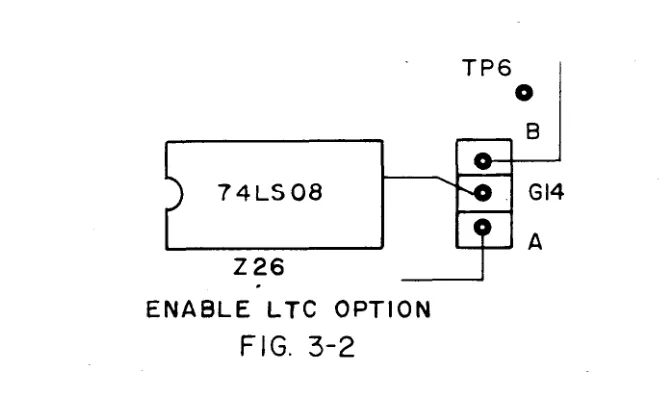
3.3.2.1 Line Time Clock
If a remote Line Time Clock switch is used on the front panel, then specific jumpers are required to be installed on the TBC module.
The line time clock options are factory set to allow software enabling of the LTC using the jumper from G14 to G14A. The jumper is actually a printed circuit foil between G14 and G14A on the solder side (bottom) of the TBC module. To convert to a manual (external) line time clock switch, the foil between G14 and G14A on the solder side of the module must be cut and a wire jumper installed between G14 and G14B. The holes have been placed on .1 inch centers to allow for the use of wire wrap pins and jumper plugs by the user in the event that the option is changed frequently.
74LS08
Z26
ENABLE LTC OPTION
FIG. 3-2
TP6
o
8
GI4
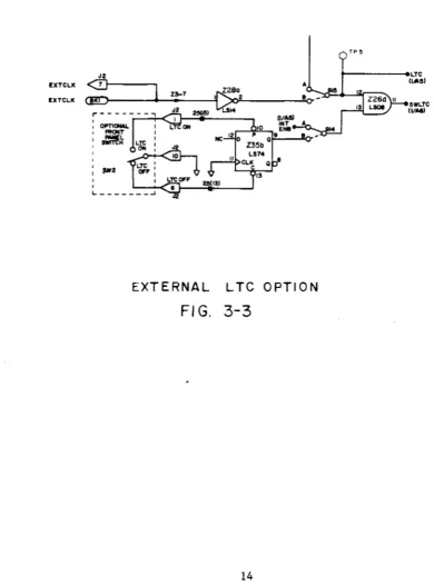
The clock signal supplied to the module can be generated from internal or external sources. Internally, the signal comes from the circuitry which de-tects the AC signal from a remote 24 VAC center-tapped transformer, converts is to logic pulses in step with the power line frequency, and applies it to point G15A. The factory setting is a foil between Gl5 and GI5A. To use the external clock, the foil between Gl5 and G15A is cut and a jumper wire added between G15 and G15B. The external clock can be supplied from QBUS pin BKI or the front panel cable connector J2 pin 7.
EXTCLK
EXTCLK
~
1
,...---,
I
OPTIONAL fIIONT
J:tI!k
Z~7
•
J2 2eGlI)
1~.=.2---::.
LSI4I t -... ---~
L ON 10
NC 12 D
EXTERNAL LTC OPTION
FIG. 3-3
TRC11 User's ManuaI
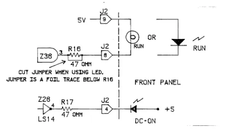
3.3.2.2 LED and Lamp Options
Two options are available for front panel indicators. The RUN lamp is driven directly by a 75451 line driver. The circuit contains a 47 Ohm re-sistor for use with an LED instead of the normal incandescent lamp. The resistor (R16) has a shorting foil etched across it, which can be seen on the solder side of the module directly beneath R16. To use an LF.D on the front panel, cut the shorting foil. This provides current limiting for an LED indicator.
J2
5Y
OR
3
R16
Z38
v..----I~
47
OHMCUT JUMPER WHEN USING LED.
JUMPER IS A FOIL TRACE BELOW R16
FRONT PANEL
+5
LS14
DC-ON
Figure 3-4 LED and Lamp Options
/'V'
RUN
Note: The optional indicator for DC ON is factory set for proper operation of an LED.
Note: See section 2.3 for definit10n of SRUNL, which is used to operate the RUN indicator.
3.3.2.3 Boot Option
3.3.3 AC Power
The Line Time Clock requires an AC signal from the power line in order to generate an interrupt on the BEVNT L line. (The clock signal may also be supplied from an external source. See paragraph 3.3.2.1)
For systems supplied by General Robotics Corporation, a small 24 VAC, center tap transformer is used to supply signals to the clock detect logic. The wires from the transformer are tied to connector J1. See Table 2.3.2
Signals from the transformer are also used to detect AC power failure, and are required to operate the TBC properly. BUS signals BDCOK and BPOK are generated on the TBC, and are used in power up sequencing. It is mandatory for proper system operation, to provide the required AC signals to J1. The user may supply his own source of AC, as long as it conforms to specificati-ons given in Section 2.2.2. See Figure 3.5 for diagram of circuit board components. These parts may be ordered through the General Robotics Sales Office as a complete assembly.
(10 ") BROWN
~
BL~
BRf'VWHT
~
BLU
(24")
,--O_R_G __ 24 VAC
WHT/ORG NEUTRAL---I
,---L-..::...:...~
ORG
" " " - - - 2 4 VAC----'
FI G. 3-5
PiN 630-0005-00 Transformer,115/230V,24V CT,LTC
TBC
PiN 676-0020-00 Connector,free hanging,3 pin,locking,male shell
AC INPUT
BPOK H
BDCOK H
DC
VOLTAGES
/
---TBCll User's Manual
( (
1/
\
( (
--iJomSr
I
I~I
1
Minimum
140 mS
L
j6mS
I
C I
I
' J1
6mJ-
--110ms
c (
Minimum
/
/1Power-Up Sequence
Power-Down Sequence
Power Signal Generation Timing Figure 3-6
r
3.3.4 PROMS
Space is provided for two 8-bit EPROMS or PROMS to be used for a bootstrap. Their addressing is set to respond to 773000(8) with a window size of 256(10) words. The window size may be changed to 512, 1024, or 204R words and the address may be placed at any multiple of the window size in the I/O page by modifying a set of jumpers on the board. EPROMS of the 2704/2708/2716 family or equivalent may be used. General Robotics offers several standard EPROM sets which bootstrap multiple devices including RX02, RK05, RP02, RL02, many 8" and 5 1/4" winchester disk subsystems, SMD disk subsystems, and non-standard high density floppy disk subsystems. Custom EPROM sets are available on special request at additional charge. Options also provide for changes in the EPROM starting address and the window size in the memory map.
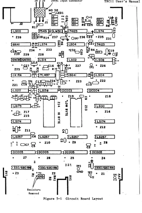
To enable the bootstrap, connect the two test points at G12 and G12R with the jumper clip.
To disable the bootstrap, either:
1) Remove the jumper clip connecting G12 and GI2B, or, 2) Install the clip on only one of the test points.
See Figure 5-1 for location and identification of G12 jumper. The following Tables provide information related to PROM options.
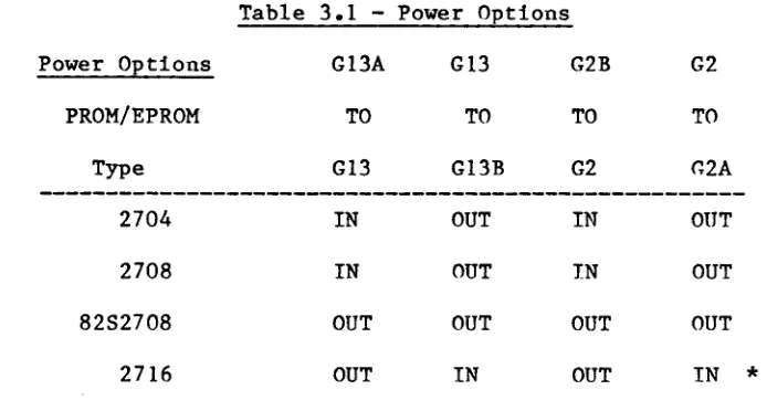
Table 3.1 - Power Options
Power Options G13A G13 G2B G2
PROM/EPROM TO TO TO TO
Type G13 G13B G2 G2A
---2704 IN OUT IN OUT
2708 IN OUT IN OUT
82S2708 OUT OUT OUT OUT
2716 OUT IN OUT IN *
TBCII User's Manual
Table 3.2 - PROM Starting Address
PROM G6B G6 GIA GI G8A G8 G7B
Starting TO Address G6
TO TO TO TO G6A GI GIB G8
TO TO G8B G7 OOXXXX OUT IN OUT IN OUT IN OUT 01XXXX OUT IN OUT IN OUT IN IN 02XXXX OUT IN OUT IN IN OUT OUT 03XXXX OUT IN OUT IN IN OUT IN 04XXXX OUT IN IN OUT OUT IN OUT 05XXXX OUT IN IN OUT OUT IN IN 06XXXX OUT IN IN OUT IN OUT OUT 07XXXX OUT IN IN OUT IN OUT IN 10XXXX IN OUT OUT IN OUT IN OUT llXXXX IN OUT OUT IN OUT IN IN 12XXXX IN OUT OUT IN IN OUT OUT 13XXXX IN OUT OUT IN IN OUT IN 14XXXX IN OUT IN OUT OUT IN OUT 15XXXX IN OUT IN OUT OUT IN IN 16XXXX IN OUT IN OUT IN OUT OUT 17XXXX IN OUT IN OUT IN OHT IN
G7 TO G7A IN OUT IN OUT IN OUT IN OUT IN OUT IN OUT IN OUT IN OUT NOTES 1,2 2 1,2 1,2 2 1,2 1,2 1,2 2 1,2 1,2 2
1,2
*
XXXX=
SEE TABLE 3.3. *Normal Factory SettingIMPORTANT NOTE: Starting with the Rev. C TBC, BBS7 enters into the equation for the starting address, which limits the PROM/EPROM starting address to the I/O page (760000 to 777777). If addressing in the range 000000 to 177777 is required, cut run to Z20 pin 5 and connect pin 5 to pin R, and use above Table.
NOTES:
1. Starting address not available for 2708, 2716, etc. with window size of 1024. See Table 3.2. (Both G7 links out.)
2. Starting address not available for 2716, etc with window size of 204R.
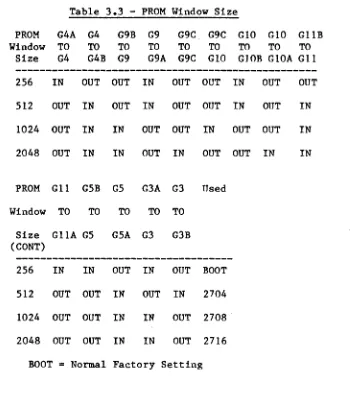
Table 3.3 - PROM Window Size
PROM G4A G4 G9B G9 G9C G9C GI0 GI0 GlIB Window TO TO TO TO TO TO TO TO TO
Size G4 G4B G9 G9A G9C GI0 GlOB GI0A GIl
---256 IN OUT OUT IN OUT OUT IN OUT OUT 512 OUT IN OUT IN OUT OUT IN OUT IN 1024 OUT IN IN OUT OUT IN OUT OUT IN 2048 OUT IN IN OUT IN OUT OUT IN IN
PROM GlI G5B G5 G3A G3 Used Window TO TO TO TO TO
Size GlIA G5 G5A G3 G3B (CaNT)
---256 IN IN OUT IN OUT BOOT 512 OUT OUT IN OUT IN 2704 1024 OUT OUT IN IN OUT 2708 2048 OUT OUT IN IN OUT 2716
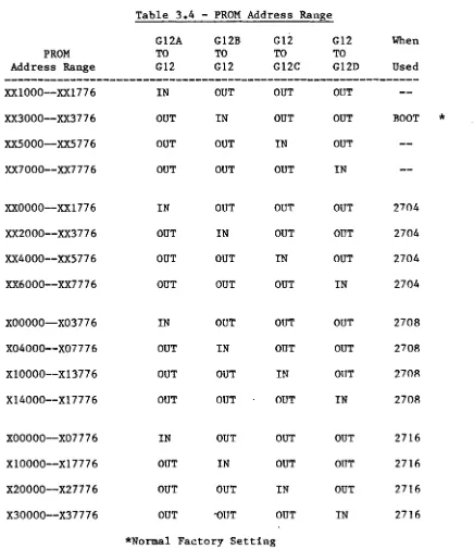
PROM Address Range XXI000--XXI776 XX3000--XX3776 XX5000--XX5776 XX7000--XX7776 XXOOOO--XXI776 XX2000--XX3776 XX4000--XX5776 XX6000--XX7776 XOOOOO-X03776 X04000--X07776 XI0000--XI3776 XI4000--X17776 XOOOOO--X07776 XI0000--XI7776 X20000--X2 7 77 6 X30000--X37776
Table 3.4 - PROM Address Range G12A TO G12 IN OUT OUT OUT IN OUT OUT OUT IN OUT OUT OUT IN OUT OUT OUT G12B TO G12 OUT IN OUT OUT OUT IN OUT OUT OUT IN OUT OUT OUT IN OUT 'OUT G12 TO G12C OUT OUT IN OUT OUT OUT IN OUT OUT OUT IN OUT OUT OUT IN OUT *Normal Factory Setting
3.3.5 Software Registers
G12 TO G12D OUT OUT OUT IN OUT OUT OUT IN OUT OUT OUT IN OUT OUT OUT IN
TBCll User's Manual
When Used
BOOT *
2704 2704 2704 2704 2708 2708 2708 2708 2716 2716 2716 2716
Since RT-11 V02 does not turn on the clock, this may be done by (1) Booting the system, (2) Halting the system, (3) Accessing location 777546, (4) Inserting the value 100 into it, and (5) Typing P to continue. Note that any time a "G" from ODT or a bus reset instruction is executed, the clock will stop and must be manually restarted.
The LTC control register is at octal address 777546 with contents as shown below:
LTCCSR: 777546
15 14 13 12 11 10 9 8 7 6 5 4 3 2 1
o
I 0 I 0 I 0 I 0 I 0 I 0 I 0 I 0 I MON I IE I S I 0 I 0 I 0 I 0 I 0 I
BITS DESCRIPTION 15-8 Zero - Not Used.
7 MON - Monitor is set when a line time clock (LTC) pulse has occur-red (every 16.67 ms for 60 hz and 20 ms for 50 hz). Reset by writing a "0" into Bit 7 or by BINIT L. Read only.
6 IE - Interrupt Enable, when set, enables interrupts from LTC. In-terrupt is generated on either the BEVNT L line or the BIRO L line, depending on the state of Bit 5. Reset by writing a "0" into Bit 6 or by BINIT L. Read/Write.
5 S - Select, when set along with Bit 6 and an LTC interrupt occurs, activates the BIRQ L line. A vector of 100(8) is generated when the processor responds. When reset, under the same conditions as above, the BEVNT L line is activated. Reset by writing a "0" into Bit 5 or by BINIT L. Read/write.
4-0 Zero - Not used.
The first indication that the Line Time Clock is properly working is when correct AC and DC power is applied to the TBC module. The DC ON indica-tor(LED) should light. The circuits which generate the power sequence signals utilize some of the same circuits for the Line Time Clock.
After booting the system, the Line Time Clock can be tested by using the RT-11 Monitor command for displaying time. The command under RT-ll Ver-sion 3 (or later) is: .TIME (Carriage Return)
The response for time is: The format for time is: 3.3.6 Backplane Position
00:00:00 HH:MM:SS
TBel1 User's Manual
CD
·Ad3~1
Z17==
-<
-t
Z15 m
CD
) LSI14 -< -t
m
~(Jt
Zl1~O
0
~LS251 IC6 ~LS257
I
no) LS257:>. :>
OC7.<al
•
ZlOw • Z9
--
..
~ DC005
I
~DC005- I)
DC005•
Z7•
Z6•
Z5) 330/680
RNI
:> ) 330/680 RNI
• Z3..
Resistors Re.oved
Z2
N ~ ~
:g~n~
TP3
o
GND
Z18
) LSOO
•
Zl6) LSI74
• Z12
) LS2Q7
• :> ZI
:> Co>
•