I
I
~~~
I
I
I
PROCESSOR
I
:~:RAGE
i
i
I
I
Ii1 g J ~
This manual is published by the Uni vac Di vision of Sperry Rand Corporation in loose leaf forma t. This forma t provides a rapid and complete means of keeping recipients apprised of UNIVAC ® Systems developments. The infor-mation presented herein may not reflect the current status of the programming effort. For the current status of the programming, contact your local Univac Representati ve.
The Univac Division will issue updating packages, utilizing primarily a page-for-page or unit replacement technique. Such issuance will provide notification of software changes and refinements. The Univac Division re-serves the right to make such additions, corrections, and/or deletions as, in the judgment of the Univac Division, are required by the development of its Systems.
UNIVAC is a registered trademark of Sperry Rand Corporation.
This document was produced using UN ADS. This system has been developed by the Applications Section of Product Support Operations as a research proJect for the Systems Programming Department of the Data Processing Division of Univac.
UP·7627 418·111 PROCESSOR AND STORAGE Contents 1
SECTION: PAGE:
CONTENTS
CONTENTS 1 to 3
1. INTRODUCTION 1-1 to 1-1
2. MAl N STO RAGE 2-1 to 2-2
3. COMMAND/ARITHMETIC SECTION 3-1 to 3-13
3.1. INTRODUCTION 3-1
3.2. REGISTERS 3-1
3.3. DESIGNATORS 3-2
3.4. INSTRUCTION TYPES AND FORMATS 3-3
3.5. ADDRESSING 3-5
3.6. STORAGE PROTECTION (GUARD MODE LIMITS) 3-B
3.7. PRIVILEGED INSTRUCTIONS 3-9
3.B. FLOATING POINT NUMBERS 3-9
3.9. INTERRUPTS 3-10
3.9.1. Parity Fault Interrupts - Locations 2181 228 1 2781 3181 3281 and 408 3-10 3.9.2. Supervisor Call Interrupt - Location 208 3-11 3.9.3. Day Clock Interrupt - Locations 23 8 and 248 3-12 3.9.4. Real Time Clock Interrupt - Locations 258 and 268 3-12 3.9.5. Guard Mode Interrupt - Location 308 3-12 3.9.6. Power Loss Interrupt - Location 338 3-12 3.9.7. Floating Floating Point Underflow Interrupt - Location 348 3-12 3.9.B. Floating Point Overflow Interrupt - Location 358 3-12 3.9.9. Interrupt Lockout Timeout Interrupt - Location 418 3-12 3.9.10. lSI Extemal Interrupts - Locations 14°8-1778 and 24°8-2778 3-13 3.9.11. lSI Internal Interrupts - Locations 1°°8-1378 and 2°°8-2378 3-13 3.9.12. ESI Interrupts - Locations 368 and 378 3-13
4. INPUT /OUTPUT SECTION 4-1 to 4-21
4.1. INTRODUCTION 4-1
4.2. GENERAL DESCRIPTION 4-1
4.3. FUNCTIONAL OPERATION 4-1
4.4. CHANNEL OPERATION 4-3
4.5. I/O CHANNEL PRIORITY 4-3
4.6. INPUT/OUTPUT INTERFACE 4-4
4.7. 10M RESPONSE TIME 4-5
UP-7627 418·111 PROCESSOR AND STORAGE 4.8.1. 4.8.1.1. 4.8.1.2. 4.8.1.3. 4.8.1.4. 4.8.1.5. 4.8.2. 4.8.2.1. 4.8.2.2. 4.8.2.3. 4.8.2.4. 4.8.2.5. 4.8.2.6. 4.8.2.7. 4.8.2.8. 4.8.2.9.
Internally Specified Indexing (151)
Programmed Activation of an I/O Channel - 151 Mode 151 Buffer Control Word Formats
151 Input/Output Activity 151 External Interrupt 151 Monitor Interrupts
Externally Specified Indexing (ESI)
Programmed Activation of an I/O Channel - ESI Mode ESI Buffer Control Word Formats
Terminal Buffer Condition Halfword Terminal Buffer Condition Fullword
Terminal Condition Fullword or Halfword With Buffer Chaining ESI Buffer Termination Interrupt and External Interrupt Tabling ESI Interrupt Table Pointer
ESI Interrupt
ESI Parity Error Handling
4.8.2.10. ESI External Interrupt Word Transfers 4.9. REAL TIME CLOCK
4.10. INITIAL LOAD
5. OPERATORS CONSOLE
5.1. GENERAL 5.2. DAY CLOCK
APPENDICES
A. NORMAL AND COMPATIBLE CHANNELS
B. lSI INPUT. OUTPUT. AND FUNCTION MODE CHANNEL ACTIVITY
C. FORMAT OF RESERVED LOCATIONS
D. INSTRUCTION REPERTOIRE SUMMARY
E. MAINTENANCE PANEL
Contents SECTION: 4-6 4-6 4-7 4-9 4-10 4-10 4-10 4-13 4-13 4-16 4-17 4-17 4-18 4-19 4-20 4-20 4-21 4-21 4-21
5-1 to 5-3
5-1 5-2
A-1 to A-3
B-1 to B-3
C-1 to C-1
0-1 to 0-7
E-1 to E-4
UP-7627 418-111 PROCESSOR AND STORAGE
FIGURES
2-1. 3-1. 4-1. 4-2.
TABLES
Main Storage Allocation
Type I Instruction Addressing Techniques One I/O Channel
ESI Data Transmission
4-1. I/O Channel Control Signals
4-2. Time Between Subsystem Request and 10M Acknowledge 5-1. Console Signal Code Reference
A-1. Normal Channel Data Transfer Rates A-2. Compatible Channel Data Transfer Rates
Contents
SECTION:
2-1 3-7 4-4 4-12
4-5 4-5 5-2
A-2 A-3
3
UP-7627 418·111 PROCESSOR AND STORAGE
SECTION: 1
1. INTRODUCTION
This document describes the three individual hardware components of the UNIVAC 418-111 Real-Time System. These hardware sections and the order of their presentation are as follows:
• Main Storage
• Command / Arithmetic Section
• Input/Output Section
Section 2 of this manual describes main storage and discusses the interfacing between it, the Command/Arithmetic, and the Input/Output sections. In Section 3 the Command/Arithmetic Section is discussed in more detail, and Section 4 describes the Input/Output Section.
UP-7627 418·111 PROCESSOR AND STORAGE 2 SECTION:
2. MAIN STORAGE
Main storage is divided into four banks each consisting of one or two modules. Each module has four bays, each containing 4096 eighteen-bit words of storage. The UNIVAC 418-111 main storage is divided into 18-bit addressable words. Up to 131,072 words (4 banks, 2 modules each) may be addressed by the Command/Arithmetic section. Each storage bank has three access paths, one to the Command/Arithmetic (C/ A) Section and one to each Input/Output Module (10M). In this manner, parallel access to storage may be obtained by the C/ A and each 10M whenever each references a different storage bank. Regardless of the physical distribution of various modules, addressing is always continuous.
Figure 2-1 illustrates the parallel paths available to each bank. If any bank is being accessed by two or more of the access paths, only one at a time is honored.
BANK 0
16K
16K
I
10M #11
I
UP TO 16 I/O CHANNELS 16- 31
,
BANK 1 BANK 2
16K 16K
16K 16K
1
COMMAND
ARITHMETIC ~ SECTION
Figure 2-7. Main Storage Allocation
BANK 3
16K
16K
1
"'"1
-J
I
10M #0
I
UP TO 16 I/O CHANNELS 0-15
MAIN STORAGE
UP-7627 418·111 PROCESSOR AND STORAGE
I
.ECTION, 2In addition to the ferrite core storage, the UNIVAC 418-111 System uses several high s-peed integrated general registers (IGR) located in the 10M's. Read/restore cycle
time for main storage is 750 nanoseconds, and for integrated storage, 186 nanoseconds.
These IGR registers are assigned fixed addresses which duplicate the corresponding
core storage addresses. Locations 3008 through 4778 are the corresponding IGR and
core storage locations. The C/ A section accesses the IGR storage whenever an address in this range is specified, whereas the I/O sections address the corresponding core storage locations.
UP-7627 418.111 PROCESSOR AND STORAGE
3
SEC TIONI
3. COMMAND/ARITHMETIC SECTION
3 1.
INTRODUCTION
The Command/Arithmetic Section (C / A section) consists of the hardware necessary to enable certain functions to be performed whenever it is given control. These functions are obtained from main storage as are the necessary operands.
In addition to having access to main storage, the C / A section has certain storage registers and designators which allow it to perform its various functions. These are described only to the extent necessary for the programmer to understand how the hardware works.
Appendix D summarizes the instruction repertoire for the UNIVAC 418-111 System. For
a detailed description of each function, refer to UN IVA C 418-111 Assembler.
Programmers Reference .Manual. UP-7599 (current version).
3.2.
REGISTERS
The following is a brief description of the registers of the C / A section.
• Instruction Address Register
The Instruction Address Register (lAR) contains the address of the next instruction to be performed. The IAR is not program accessible.
• Arithmetic Accumulators
There are two arithmetic accumulators, A Upper (AU) and A Lower (AL), which can be operated upon under program control. Each accumulator is 18 bits long: they can be used jointly as one 36-bit accumulator (A register).
• Index Re.gisters
Eight Index Registers are available for use (only one at a time) as address modifiers. The index registers are program accessible and are storage locations 18 through 108 ,
• B Register
The B Register contains the contents of the active index register and is used by the hardware whenever an indexed instruction is executed. The B Register is not program accessible.
• Index Register Pointer
The Index Register Pointer contains the main storage address of the currently active index register.
1
UP-7627 418·111 PROCESSOR AND STORAGE 3
SECTION:
• Special Register
The Special Register (SR) is used to specify interbay (4K storage segment) addressing. The S R contents are under program control. (See 3.5 for description of SR operation.)
• KO Register
The KO register is used for internal purposes and is not accessible to programmed instructions; it may be inspected from the maintenance panel. During the execution of a shift instruction, KO contains the shift count.
• Z Register
The Z register is used for internal purposes and is not accessible to programmed instructions: it may be inspected from the maintenance panel. For most instructions, Z contains the operand address.
• Storage Limits Registers
Two 9-bit registers, called Storage Limits Upper and Storage Limits Lower, are used to contain the addresses of the upper and lower boundaries of an area which is protected by the Guard Mode. An area so placed under Guard Mode becomes the only area in wh ich the C / A sect ion may cause the contents of any locat ion to be changed. The Storage Limits Registers are loaded as a result of the LGM instruction.
3.3.
DESIGNATORSThe following is a description of the designators of the C / A section.
• Compare Designator
The Compare Designator is a bi-stable, three-stage register whose state is determined by the execution of any of the COMPARE instructions (f = 02,03,06,07). The
results of the COM PARE instructions are recorded by the Compare Designator as follows:
The COMPARE stage IS set upon the execution of any of the COMPARE
instruct ions.
- The LESS THAN stage is set if a COMPARE instructions finds (AL) less than the contents of the addressed storage location (f = 02, 03), or [(AU)Dml(AL)] less
than the logical product of (AU) and the contents of the address storage location
(f = 06, 07).
- The EQUALS stage is set if a COMPARE instruction finds (AL) equal to the contents of the addressed storage location (f = 02, 03) or [(AU)rMm(AL)] equal
PAGE:
to tlfe logical product of (A U) and the contents of the add res sed stora ge location
(f = 06, 07).
The COMPARE stage is cleared by the execution of any instruction other than the arithmetic JUMP instructions (f = 60 through 67). Thus, if the results of a COMPARE
instruction are to be successfully tested, it must be immediately followed by one or more of the JUMP instructions.
UP-7627 418-111 PROCESSOR AND STORAGE 3
SECTION:
When the COMPARE stage of the Compare Designator is set. or while processing a COMPARE instruction, all interrupts are locked out to avoid the possibility of inadvertently clearing the COMPARE stage. It should be noted that the arithmetic JUMP instructions have significantly different operations if executed when the COMPARE stage is not set.
• Borrow Designator
The Borrow Designator is a bi-stable, single-stage element whose state is determ ined by the execution of either a double-length ADD instruction (f = 20, 21), or a double-length SUBTRACT instruction (f = 22, 23). If an end-around borrow would
be required during the execution of either of these instructions, it is inhibited and the Borrow Designator is set. The Borrow Designator remains set until the subsequent execution of another double-length ADD or double-length SUBTRACT instruction.
The condition of the Borrow Designator may be tested by the TEST NO BORRO\\,' instruction (f = 5051). When the Borrow Designator is set, interrupts are not locked out.
• Overflow Designator
The Overflow Designator is a bi-stable, single-stage clement \vh ich is set when an overflow occurs during the execution of any of the following instructions:
ADD AL (f = 14, 15)
SUBTRACT AL (f = 16, 17)
ADD A (f = 20,21) SUBTRACT A (f = 22, 23) DIVIDE A (f = 26, 27)
ROUND A (f = 5060)
ADD AL PLUS CO~ST A~T (f = 71) FLOATING POINT DIVIDE (f = 5005)
The state of the Overflow Designator is tested by either the TEST OVERFLOW instruction (f = 5052) or the TEST NO OVERFLOW instruction (f = 5053). The execution of either instruction automatically clears the Borrow Designator. When the Overflow Designator is set, interrupts are not locked out.
• Guard Mode Designator
The Guard Mode Designator is a bi-stable, single-stage element set as a result of the LGM (f = 5065) instruction. When the Guard Mode Designator is set by the LGM
instruction, any write reference to the storage area outside of the lim its set, with the exception of addresses 008 through 178 , will cause a Guard Mode Interrupt. If a privileged instruction is attempted while in Guard Mode, the function will be inhibited and a Guard Mode Interrupt will be generated. The generation of any interrupt will release Guard Mode and clear the Guard Mode Designator.
3.4.
INSTRUCTION TYPES AND FORMATS
Instructions for the UNIVAC 418-111 System have two parts, the function field and the operand field. The contents of the function field indicates to the C / A section which operation is to be performed: the contents of the operand field supplies the C / A section
3
UP-7627 418·111 PROCESSOR AND STORAGE 3
SECTION:
with the necessary information to enable it to perform the function. The instruction repertoire is the set of all recognized functions.
The UNIVAC 41S-III instructions fall into three distinct types, designated I, II, and III. Type I instructions are identified by function codes 02 through 27, 32, 33, and 40 through 47. Type II instructions are identified by function codes 30, 31, 34 through 37, and 51 through 76. Type III instructions are identified by function codes 5000 through 5077.
• Type I Instructions
The Type I instruction format is:
u
where: f is the six-bit function code
u is the 12 low-order bits of the operand address.
• Type II Instructions
The Type II instruction format is:
u or z
where: f is the six-bit function code
u is the 12 low-order bits of the operand address
z is the 12 low-order bits of an IS-bit sign-extended operand.
When f indicates that the 12 low-order bits are to be interpreted as the actual operand, PAGE:
the IS-bit operand is formed by using z and propagating the contents of bit 11 to the six high-order bits. This is commonly referred to as sign extension.
• Type HI Instructions
The characteristic of a Type II I instruction is the use of a major function code of 50 and a minor function code between 00 and 77. Type III instructions may be subdivided into two distinct categories, each with a slightly different format.
UP-7627 418-111 PROCESSOR AND STORAGE 3
SECTION:
Type III-a
m K
where: f is 50
m is the minor function code
K is zero or a constant less than 64.
Type II I-b
f m Unused
17 12 11 6 5 0
Unused I u
17 13 12 11 0
where: f is 50
m is the minor function code
I is 0 if index ing is not used
I is 1 if index ing is used
u is the 12 low-order bits of the operand address.
Type III-b instructions are 2-word (36-bit) instructions.
In addition to the foregoing formats there are several Type I II-a instructions which use the contents of one or more storage locations following their occurrence for specific data. These are principally the I/O instructions. Control is transferred to the storage location following the data words used by them.
3.5.
ADDRESSINGThe operand fields of Type I, Type II, and Type II I-b instructions contain 12 bits. The UNIY AC 418-111 main storage is logically divided into bays, each containing 4096 eighteen-bit words, and may be expanded to a maximum of 32 bays: therefore, each Type I, Type II, or Type III-b instruction provides sufficient space to specify any address within a bay. The bay which contains the desired address is determined by certain rules outlined in the following discussion.
When an instruction is executed which is in the last storage location of a bay, program control passes to the first location of the next bay unless it is a skip or jump type
UP-7627 418·111 PROCESSOR AND STORAGE
I
3SECTION, PAGE:
instruction. If it is a skip type instruction, control passes to the first or second location of the next bay depending on whether or not the skip condition is met. If it is a jump type instruction, control passes to the storage location specified in the next bay. This is tantamount to saying that as long as forward jumps are made, it does not matter where the instruction is located in storage.
In order to enable certain instructions to access any address in storage, the SR (Special Register) may be used to specify which bay is to be used. The Special Register is active or inactive depending on whether bit 4 is set to one or to zero; bit 4 is not a part of the bay identification. Bits 5 and 3 through 0 of SR are the bay bits.
Example:
543210
To set the SR active to bay 25 (31 8 ), the binary number
Illy
11010111 (71 8) must be stored in SR because bit 4 (SR active bit) must be set to l. The desired address is derived by ignoring bit 4 and treating bit 5 as though it were in bit position 4. By doing this, 718 becomes 318 (111001 2 -+ 110012).543210
To set the SR active to bay 5 (58)' the binary number 1011101110111 (25 8) must be
stored in SR.
In order to set the Special Register active to bay 3, the instruction
LABEL OPERATION OPERAND
10 20 30 40 COM 50
l L L L 1 L_ . .L---1_ l----.l _~.L .... .1_._l __ L J _ _LJl
is executed. To set it active to bay 31 (32nd bay), the instruction
is executed. To inactivate the Special Register the instruction
may be executed.
When the C/ A section makes reference to the storage location corresponding to the index register specified in the IRP, the B Register is accessed instead (see 3.2).
When the C / A section makes reference to the addresses 3008 through 4778 , the contents of the corresponding IG R storage locat ion is accessed instead.
• Type I Instructions
Type I instructions are SR-sensitive and indexable, meaning that if SR is active, the bay specified by its contents is accessed, and that the contents of the active index register are used to modify the operand address if the function code is odd.
If SR is not active (bit 4 is zero), the bay to be accessed is that in which the instruction itself resides; the bay bits are taken from the five high order bits of the Instruction Address Register.
UP-7627 418·111 PROCESSOR AND STORAGE
LABEL
3 SECTION:
If the function code (f) is odd, indexing is specified. This means that the full IS-bit contents of the active index register are arithmetically added to the (positive) l7-bit operand address. Figure 3-1 illustrates the various addressing techniques for Type I instructions.
OPERATIO~ OPERA~D
10 20 30 40
PAGE:
COM~ 50
_ L 1 L..L .. J i ~L-.L~.1~J~l .. L.LJ . .-.LL ... .L 1 Qt_L 1 .1. ... L L .... L L . 1 1~ I1..J1 IN iE I 11.J.-L.LL.L L..l 1 .. 1 . .1 1 I 1 I
1._.l 1 1 1. I. J.. ... LLU~L~L.J L .. 1 .. 1... .. L.-.1. L I OLLO ~LL .. I L I .1 ['_1
LJ
L~LI;L L2J . L .ll .. L...L L I ~ .• j I 1 I 1._1 .1 1 I 1_1 ..~~~~~~~~~~~~~~~~~~~~~~~~~~~~~
__
~~~~~~~~~-L... L .. .1 .LL.1J_1..i...Ll!-.lBLLJ. __ L.1_.-..L..L..L.-l~~_L~.~~i~) . . L . l l·.L~L~.lN, EI...L6L J. I 1 .... LL...L...L L1.1 1 L L
1.1. LL.LLLJ.Llh~L.J...LL L.LL . .L~'h!L~L.L .. L...LL1.~...J-illNL~L.L~.1_1L.L L l .1._1...J.l I I I
I .L.LL ... LL....L...L...L.lh S.,-I R---'-I---'-...L...LL..L.L.JQ.l!i~L_LL.L_L_L_Ll~ . .LL1~.L~L ~.L.L ~L...l...LL . . L.L 1 L ; I L I I
.L.L.L .... L. __ LL.L ... 1 .. L L~LI..LL.I ~-'----..LI. L..L.L.J.~~.L<!lOL.LL_L_Ll'....JI...J.i~lEi . .1.~.L . .l._.l. .L . .L...L_L.l 1 1 L 1
l_l_L.L. . .l .. ...L.J. .. LL.-I . ...L...L.L...L.L. I I I L 15..J.R.L.i_L_L_L..i_.1 10 I I 1 I .L...L.l...L...LL..Lb.ili&~L1.L.h_L j ._..L.L.L.L_L.L . ....L..-L.. L L.L..L.. Li_.L....L...LJJ....tIiL .L.L_LL.-L_L.L.-.l~L'o..Ll.LQ.Jh"<L.-O....t.l.L-LJ.b.J..1~ 13 1 I I I L - l .. L.L1 __ .1 L I
_.L...L..L..L.L...L.L.l6L1 1 I 1 I L~ I 1*101 1 10101 1 1 1 I I. I LII 1 N, EI 1114LL...L..1 I I
I.Li~_L.Ll.-Figure 3·1. Type I Instruction Addressing Techniques
If line were to be located at address 020000, the following storage references would be made:
LINE NO. EFFECTIVE U ADDRESS REFERENCED
2 0100 + 020000 020100
4 0100 + 030000 030100
7 0100 + 020000 + 030000 050100
9 0100 + 000000 + 030000 030100
11 0100 + 030000 + 030000 060100
14 0100 + 020000 - 010000 010100
• Type II Instructions
Type II instructions are never S R sensitive, differing in this respect from Type I instructions. Regardless of the contents of SR, the bay referenced is the one in which the instruction resides.
UP-7627 418·111 PROCESSOR AND STORAGE 3
SEC TION: PAGE:
Some Type II instructions are index sensitive: this allows them to access other bays by using the active index register to modify the address obtained by combining U11-0 and IAR 17-12 "
Three instructions (LBK, LLK, and ALK) do not make a second storage access. The sign-extended value of the operand field is used as the operand .
• Type III instructions
The Type III-a instructions do not require an operand. The Type III-b instructions resemble the Type I instructions: they are SR and index sensitive. When I is set to L indexing is used: when it is set to 0, no indexing is used.
3.6.
STORAGE PROTECTION (GUARD MODE LIMITS)
To ensure program protection, a selected area of storage may be placed under Guard
Mode Limits through the use of the LGM (f = 5065) instruction. When the Guard
Mode is act ive, any attempt to store into a storage address outside the range set by the LG M instruction causes a Guard Mode Interrupt at address 3°8 " Two 9-bit registers, Storage Limits Upper and Storage Limits Lower, may be loaded with the upper and lower bounds of an area of storage to be placed under Guard Mode. For this purpose, storage is divided into 256-word blocks. The LGM is a privileged instruction and may not be used by the programmer.
When the nine high-order bits of a 17-bit storage address are placed in Storage Limits Lower, the first address of that block is the lower bound of the Guard Mode Limits. When the nine high-order bits of a 17-bit storage address are placed in Storage Limits Upper. the last address L)f that block is the upper bound of the Guard Mode Limits. For example, the instruction
LABEL OPERATION OPERAND
10 20 30 40
1 l 1 l L1G1Ml 1 l 1 1 ! 1 1
_ . .1.l , 1 i I j 1 L_l. .;. ____ -l.
prevents storage outside the range of addresses 0774008 to 01377778; any attempted violation of this restriction causes a Guard Mode Interrupt instead.
000
~
III liDO 000~_~
________
~~!_7
________________
~0
address 077400
0177
=
Storage-Limits -Lower Contentsaddress 0137777
~
Ol
011 IIIlill
---r---;-I
17 ~ 8:7
111 111
o
0277 = Storage-limits-Upper Contents
Upon the occurrence of any interrupt, the Guard Mode Designator is cleared (disabled), so that all of main storage becomes accessible to subroutines gaining control through the
UP-7627 418.111 PROCESSOR AND STORAGE
3 SECTIONI
interrupt locations.
Because locations 0 through 178 are never under guard mode protection, it is always possible to use them for storage. The index registers are part of that category and are actually located at addresses 1 through
1°
8 ,3.7.
PRIVILEGED INSTRUCTIONSPrivileged instructions arc those which are needed by an operating (controlling) system in order to perform its job; they are considered inappropriate for use in normal (user) programs. The appearance of any of these instructions in any user program would have an unpredictable and probably disastrous effect.
When the Guard Mode Designator is set, through the use of an LGM instruction, any attempt to execute a privileged instruction causes a Guard Mode Interrupt instead. The privileged instruction is not executed or initiated.
The privileged instructions are:
5011 Load Input Channel (L IC) 5012 Load Output Channel (LOC)
5013 Load External Function Channel (LFC) 5015 Stop Input on Channel (STIC)
5016 Stop Output on Channel (STOC) 5021 Test Input Channel (TIC) 5022 Test Output Channel (TOC) 5023 Test Funct ion Channel (TFC) 5024 Wait For Interrupt (WFI) 5025 Wait For Interrupt (WFI)
5056 Stop On Key Setting (SK) - Ignored when in Guard Mode. 5065 Load Guard Mode (LG M)
5066 Set Audible Alarm (SAA) 5067 Enable ESI Interrupts (EEl)
3.8.
FLOATING POINT NUMBERSFloating point numbers are 2-word, 36-bit constants; they consist of a mantissa and a characteristic. The format of a floating point number is:
c
where:
s is the sign bit
c is the 8 characteristic bits m is the 27 mantissa bits.
PAGEl
The mantissa (m) contains the 27 significant bits of the floating point number. The magnitude of the mantissa is either zero or between .48 and .7777777778 , normalized so that the most significant bit is a one. The characteristic is the value of c in the expression 2 c-20 08*m. The high-order bit of c (bit 34) is the sign bit of the characterist ic. When c34 =1, the characteristic is positive; when c34 =0, the characteristic is negative. The sign bit (s) is zero when the floating point number is greater than zero ('positive); it is one when the number is less than zero (negative). The magnitude (positive equivalent) of a
UP-7627 418·111 PROCESSOR AND STORAGE
ISEcnoN'
negative number is its one's complement.
rake, for example, the number 2.0. It can be rewritten in floating point form as:
2.0
*
10 0 , or20.
*
10-1, or.20
*
10 1 , and many others.3
In the above examples, 0, -Land 1 are the characteristics: 2.0, 20., and .20 are the mantissas. The three expressions represent the same quantities, illustrating that the mantissa and characteristic may be manipulated so that the value of the number remains unchanged. The octal representation of this number is:
2.0
*
10 0 = .2 8*
2 3To no rmal ize, the mant issa is m ult ipl ied by 2, and the characterist ic is decreased by one.
The floating point format is:
0024000000008
Finally, to indicate that the power of the character!'.t ic is positive, the characteristic is biased to obtain 2024000000008 , In the same manner, -2.0 is represented as 575377777777 8 ,
3.9.
INTERRUPTS
3.9.1.
Interrupts are internally generated signals which cause the e / A section to interrupt its normal sequence of instructions (governed by Instruction Address Register contents), and to take the next instruction from a predetermined address in main storage. The contents of the IAR are not changed until the interrupt instruct ion is executed. An SLJ or SLJ I instruction is placed in the interrupt locations, which captures the value of IAR in order to allow normal processing to continue when the interrupt processing coding is completed.
Whenever an interrupt is generated and control passes to the appropriate interrupt location, the Guard Mode designator is cleared, and all subsequent interrupts are held back until the e / A section executes an AA I or EJ I instruction.
A summary of all reserved storage locations, including the interrupt locations, IS
contained in Appendix e.
Parity Fault Interrupts - Locations 2181 2281 2781 3181 3281 and 408
Parity errors, whenever they occur during an access of storage by either the e / A or the I/O sections, result in an interrupt. If a parity error occurs when the e / A section accesses main storage, the instruction at location 278 is executed. If a parity error occurs when the e / A section accesses IG R storage, the instruction at location 408 is executed.
If a parity error occurs when the I/O section accesses either main storage (data transfer) or IGR storage (BeW's), the address of the storage location which was being read is placed in locations 228 and 328 for 10M # 0 and 10M # 1 respectively and s the instruction at location 218 or 318 is executed, depending on whether 10M # 0 or 10M
UP-7627
3.9.2.
~n8·111 PROCESSOR AND STORAGE
3
SECTION: PAGE:
# 1 was doing the transfer.
Detection of a C / A storage parity error results in execution of the instruction at address 27 8 . This may be the result of a fault at either of two possible locations in storage. It could be the address at which the next instruction is located, or it could be the address referenced as a result of the operation being performed. In order to determine the address referenced, the following sequence is used:
(1) If a parity error occurs when reading the contents of the captured IA R address (captured through an SLJ instruction at location 278)' the error has occurred at the captured IAR address.
(2) If the parity error did not occur at the captured IAR address, a main storage search must be initiated. Instead of reading all of storage to determine which address might possibly have been referenced by some instruct ion, or instead of trying to find which effective address the interrupted instruction had referenced, a special hardware sequence can be in it iated.
An LaC instruction to Channel 0 can be performed with the BC W's set to the range to be tested (between 000000 and 1777778). Channel 0 scans the first 65K of storage until an error is found.
When an error is detected, 10M # 0 stores the address of the error in storage location 228 and interrupts the C / A section and causes it to read the instruction from storage
address 21 8. Address 218 contains a jump to the 10M #0 parity subroutine, which
captures and evaluates the address of the parity error.
Channel 0 does not scan beyond the point of error until the subroutine releases the interrupt lockout. The 10M then resumes scanning the remainder of storage starting at the ERROR location
+
2 for parity errors; the address following each error is not checked. Channel 0 can scan 65K of storage in approximately 50 milliseconds or more.If it is desired to scan upper storage (65K - 131K), the monitor interrupt from the foregoing instruction is used to reinitiate the LaC on Channel 0 with the BCW's set to the range to be tested (between 2000008 and 3777778).
NOTE: If an error occurs during the read of a jump instruction, the
instruction has been executed. If a LaC is used on channel 0, the C / A is locked out during the transfer time, because the 10M now operates at the maximum transfer speed (1.33 million words per second).
Supervisor Call Interrupt - Location 208
When an instruction with the function codes 00, 01, 77, 5000, 5001, or 5077 is attempted, the instruction at location 208 is executed. If the optional hardware for the convert or floating point instructions is not present, these function codes also cause a Supervisor Call Interrupt whenever they are executed.
UP-7627 418-111 PROCESSOR AND STORAGE
SECTION: 3
3.9.3.
Day Clock Interrupt - Locations 238 and 2483.9.4.
3.9.5.
3.9.6.
3.9.7.
3.9.8.
3.9.9.
When the Day Clock is attached, location 248 is incremented every 6 seconds. Every minute an interrupt at location 238 is generated.
Real Time Clock Interrupt - Locations 258 and 268
The Real-Time Clock (RTC) decrements the contents of location 268 every 200 microseconds. When the contents of location 268 becomes zero, an interrupt at location 258 is generated, and the contents of location 268 become 7777768 .
Guard Mode Interrupt - Location 308
When the Guard Mode designator is active and an attempt is made by the C / A section to store into a main storage or IG R locat ion wh ich is outside the I im its specified by the storage limits registers, the instruction at location 308 is executed instead of the attempted store instruct ion.
When the Guard Mode designator is active and one of the privileged instructions IS
attempted, the interrupt is generated and the instruction is not executed.
Power Loss Interrupt - Location 338
A Power Loss Interrupt results from loss of input power. The Operat ing System then has at least 0.6 millisecond to store any vital information prior to stopping. When the interru pt is generated, control passes to locat ion 338·
Floating Floating Point Underflow Interrupt - Location 348
When a floating point instruction is executed and the resulting characteristic has a value of less than zero, a floating point underflow interrupt is generated which causes the instruction at location 348 to be executed.
Floating Point Overflow Interrupt - Location 35 8
When a floating point instruction is executed which would cause the resulting characteristic to have a value greater than 3778 , a floating point overflow interrupt is generated which cause the instruction at location 358 to be executed.
Interrupt Lockout Timeout Interrupt - Location 418
If the C / A section does not release the interrupt lockout within the period of time set by the timeout delay, wh ile in Guard Mode, control is passed to location 41 8 , and the instruction previously stored there is executed. The timeout delay is approximately 100 to 200 microseconds.
UP-7627 418·111 PROCESSOR AND STORAGE
3
SECTIOI~:
3.9.10. lSI External Interrupts - Locations 14°8-1778 and 24°8-2778
When a peripheral device connected to an lSI channel transmits an External Interrupt (through the EI signal), the data transmitted is placed in location 1608+CHNO or 2608+-CHNO-16, and the instruction located at address 1408+-CHNO or
2408+CHNO-16 is executed. CHNO represents the channel number by which the
device is attached to either 10M #0 or 10M # 1 respectively.
3.9.11. lSI Internal Interrupts - Locations 1 008- 1378 and 20°8-2378
As a result of the Monitor bit in the BCWT location, each 10M generates an Internal Interrupt whenever the BC W's become equal and the IS I Internal Interrupt locat ions receive control as a result. There is one interrupt location for each channel of each 10M for both input and output.
3.9.12. ESI Interrupts - Locations 368 and 378
When an ES I table entry is made, an ES I interru pt is generated whenever the ES I interrupt lockout designator for that 10M is enabled. If interrupts are withheld as a result of any previous interrupt or PAl instruction, the ESI interrupt is delayed until interru pts are again enabled.
If the ESI interrupt lockout designator is set, no ESI interrupt is generated as a result of a new ESI table entry. Depending on which 10M is updating the ESI table, an ESI interrupt causes the instruction at location 368 or 378 to be executed and the ES I interrupt lockout designator for that 10M to be set.
UP-7627 418-111 PROCESSOR AND STORAGE
4 SECTION:
4. INPUT/OUTPUT SECTION
4.1.
INTRODUCTIONThis section provides a description of the Input/Output Section of the UNIVAC 41S-1I1 Real-Time System. It presents a detailed definition of the data transfer characteristics and of the functional operation of the Input/Output Section. A thorough knowledge of the Input/Output Section is necessary to take full advantage of the operating capabilities of the system.
4.2.
GENERAL DESCRIPTIONThe Input/Output Section consists of one or two functionally independent Input/Output Modules, 10M # 0 and 10M # 1. Each 10M is designed to permit I/O data transfers to be independent of the operation of the Command/Arithmetic Section of the UN IV AC 41S-11 I System. See Section 2 for interface with main storage.
Input/Output Module 10M # 0 has at least eight I/O channels: this number may be
increased to 16 in groups of four. Expansion beyond 16 channels to a maximum of 32 requires the addition of 10M # 1. 10M # 1 can be added with or without expansion of
10M # O. Except for the following, both Input /Output Modules are functionally
identical.
• 10M # 0 contains the logic for decrementation of the Real-Time Clock and generation of the Real-Time Clock Interrupt.
• 10M # 0, channels 0 and 1, contains the logic for communication with the day clock and the operator's console.
• Channels 16 and 17 of 10M # 1 can operate in paired channel mode only.
4.3.
FUNCTIONAL OPERATIONPAGE:
All references to input or output are made with respect to an 10M. Input describes a data transfer via an input channel from a subsystem through the 10M to main storage.
Output describes a data transfer via an output channel from main storage through the 10M to a subsystem. Any number of subsystems are capable of both input and output data transfers; however, bidirectional transfers do not occur simultaneously. Each 10M contains a set of high speed Integrated General Registers wh ich are used as storage for control words. Each 10M contains from eight to sixteen IS-bit input/output channels. Depending on the peripheral subsystem, these channels can be used singly or in pairs in order to provide a broader data path. Each 10M operates independently of the other, affording two-way simultaneity of input/output and storage with an aggregate capacity of 1.33 million IS-bit word transfers per second per module. Main storage provides separate data paths to and from each 10M.
UP-7627 418·111 PROCESSOR AND STORAGE
I
SECTION, 4Each 10M provides the data paths and the control circuitry necessary for direct communication between main storage and the input/output devices. That portion of the circuitry and the data path which is necessary to connect a peripheral subsystem with main storage is called a channel. Each channel allows transfers of data in either direction between main storage and the devices on that channel. Each channel contains 36 data lines, 18 for input and 18 for output.
Most peripheral subsystems utilize both the input and corresponding output lines of the same channel. Data transfers on these subsystems may be made in either direction over a single channel, but not simultaneously. Similarly, data transfers may not occur at the
same time through two different channels on the same 10M. If, however, the main
storage buffer areas for input /output transfers through channels of different 10M's are located in different main storage banks, these data transfers can occur at the same instant. When two or more subsystems request data transfers at the same time, each 10M performs as a multiplexer with a combined transfer rate of up to 1.33 million I8-bit words per second. If there are two 10M's and separate storage banks, the transfer rate capability is 2.66 million 18-bit words.
Each 10M functions as a small processor. Programmed instructions, executed by the Command/ Arithmetic Section, load index values into the Buffer Control Words located in the 10M and also establish desired peripheral subsystem activity. From that point on, the 10M scans the input /output channels automatically, accepting data from and passing data to the subsystem at the normal rate of the subsystem. When a peripheral subsystem requests a data transfer, the contents of the Buffer Control Words for that channel are used as a main storage address, and the transfer occurs. At the same time, the 10M updates the contents of the Buffer Control Word and tests for a terminal condition. This entire operation requires only the time of one memory cycle, 750 nanoseconds. The Buffer Control Words are located in the high speed Integrated General Registers.
The number of data words transferred between a subsystem and main storage, and the address of the locations to or from which they are transferred is controlled by two Buffer Control Words (BCW) which are associated with each data transfer operation. The Initial Buffer Control Word (BCWI) contains the current storage address of the operation. As each data word transfer occurs, the BCWI is incremented or decremented by one, depending upon a bit specified in the Terminal Buffer Control Word (BCWT). The BCWT contains the last (terminal) address of the buffer. The data transfer activity stops and the channel is deactivated when the BCWI and the BCWT are equal.
Each channel operates in one of three states: input, output, or function. The input and output states are used when transferring data to or from main storage. The channel can alternate between the input and the output states on consecutive memory cycles. The function state is the means by which the Command/Arithmetic Section establishes initial communication with a peripheral subsystem and is basically an output state. During this state, the Command/Arithmetic Section causes the 10M to transfer one or more function words to a peripheral subsystem. These function words direct the subsystem to perform the desired operation.
When one or more channels are active, the 10M, independent of program control, scans the channels in decreasing numerical sequence, in search of input and output data request signals presented by a subsystem. Upon finding a data request signal on an active channel, the 10M controls the transfer of a word between a main storage location and the requesting subsystem. Consecutive transfers of data words to or from a subsystem are performed at a rate governed by the subsystem.
UP-7627 418·111 PROCESSOR AND STORAGE
4 SEC TION:
4.4.
CHANNEL OPERATIONA single channel of the Input/Output Section provides 18-bit parallel communication between the 10M and a subsystem. (See Appendix A for a description of normal and compatible channels.)
Logically combining any pair of sequentially numbered even and odd channels (4 and 5, for example, but not 3 and 4, or 5 and 6) into a single 36-bit channel allows 36-bit parallel communication between the 10M and a subsystem.
When operating with paired channels, the control lines associated with the odd numbered channel have control of all data transfers. The most significant half of the 36-bit word is carried by the odd numbered channel; the least significant half is carried by the even num bered channel.
4.5.
1/0
CHANNEL PRIORITYAlthough all I/O channels may be available for communication between the 10M and the subsystems at the same time, only one channel of one 10M is actually transferring data at any given instant. However, since the subsystem handles data more slowly than the main storage and the 10M, it is possible for the 10M to keep all or many of the subsystems operat ing s im ultaneously.
The rate of consecutive transfers of data words to or from a subsystem is governed by the
subsystem when it is ready to send or receive a data word. When two or more
subsystems are currently active, they may also be simultaneously presenting data transfer requests (ODR's, lOR's or both) to the 10M. In order to resolve the conflict of simultaneous requests, a priority control network is used within the 10M.
When an I/O scan is performed and two or more I/O data transfer requests are present, the request from the highest numbered channel is serviced first by the 10M. Any request for I/O data transfer from the same channel is skipped for one I/O scan cycle during the next I/O scan. This allows service for the lower numbered channels of the 10M. The next request serviced is from the highest numbered channel requesting service at the time of the next I/O scan. The scan for a new operation takes place 275 ns before the last pass of the current operation is complete and every 125 ns thereafter.
The following functional priorities are established in each 10M:
(1) Output Data Transfer
(2) Input Data Transfer
(3) Main Memory and IGR Parity Errors (4) Real-Time Clock Interrupt (10M # 0) (5) Day Clock Interrupt (10M # 0) (6) ES I External Interrupt
(7) IS I External Interrupt
(8) External Function Monitor or Output Monitor (9) Input Monitor
(10) I/O Instructions and arithmetic references to the high speed integrated general register (lGR) in that 10M.
UP-7627 418.111 PROCESSOR AND STORAGE
l ..
eTloNo 4
4.6.
INPUT/OUTPUT INTERFACE
Each input/output channel between main storage and subsystems is bidirectional: transfers of data and control signals may take place in either direction between main storage and the subsystem on any channel. Each channel has 36 data lines, 18 for input data and 18 for output data, to permit parallel reading or writing of full 18-bit data words on a nonsimultaneous basis. In addition to the data lines, various control lines are used for transmitting control signals between a subsystem and the I/0 Section. The lines of an I/O channel are shown in Figure 4-1 and described in Table 4-1.
SUBSYSTEM CLEAR
OUTPUT DATA REQUEST (ODR)
OUTPUT
)
OUTPUT DATA - 18 LINES(
(
OUTPUT ACKNOWLEDGE (OA) EXTERNAL FUNCTION (EF)10M SUBSYSTEM
(
INPUT DATA REQUEST (lOR) INPUT DATA - 18 LINESINPUT <
INPUT ACKNOWLEDGE (IA)
(
,
EXTERNAL INTERRUPT (EI)Figure 4-7. One 110 Channel
4
UP-7627 418-111 PROCESSOR AND STORAGE
4 SECTION:
SIGNAL ORIGIN FUNCTION
NAME
Subsystem 10M Clears subsystem on that I/O channel.
Clear
Output Data Subsystem Indicates to I/O Section that subsystem is ready to
Request receive a data or function word.
Output 10M Indicates to subsystem that a data word is on the output
Acknowledge data lines.
External 10M Indicates to subsystem that an External Function Word
Function is on the output data lines.
Input Data Subsystem Indica tes to 10M that a data word is on the input da ta
Request lines.
Input 10M Indic'ates to subsystem that a data word has been
Acknowledge accepted by I/O Section.
External Subsystem Indicates to 10M that a Status word is on the inpu t da ta
Interrupt lines.
Table 4-1, I/O Channel Control Signals
4.7.
10M RESPONSE TIME
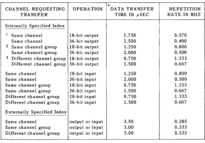
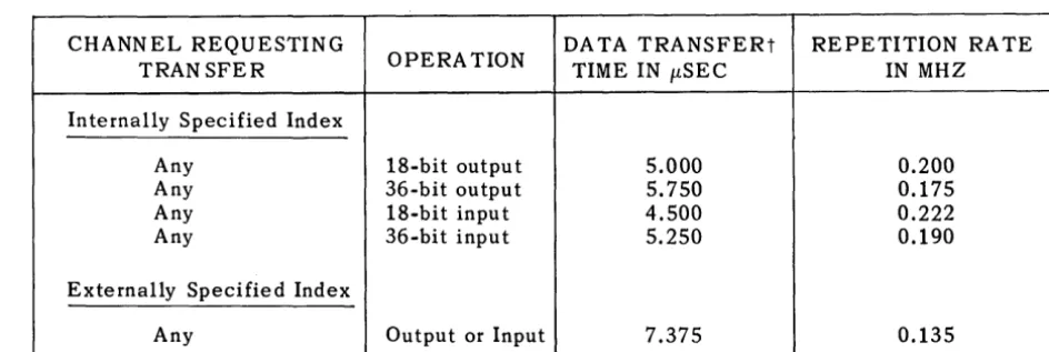
The interval between a subsystem I/0 request and the leading edge of an 10M acknowledge signal is given in Table 4-2.
OPERATION CHANNEL
COMPATIBLE NORMAL
Internally Specified Index
18 bit output 1.562 f.1sec 1.312 f.1sec
36 bit output 2.312 f.1sec 2.062 f.1sec
18 bit input 0.687 f.1sec 0.687 f.1sec
36 bit input 1.437 f.1sec 1. 437 flsec
Externally Specified Index
Output or Input 2.937 f.1sec 2.937 f.1sec
Table 4-2. Time Between Subsystem Request and 10M Acknowledge
4.8.
OPERATING MODES
A channel in the I/O Section can operate in either one of the two following modes.
uP.7_6_2_7 __
1
_______
4_1_s-_I_II_p_R_o_c_E_s_s_o_R_A_N_D __
sT._O
__
RA
__
G_E ______
~
__________
~ls~E~C~TI~ON~:
___
4 __
.I~p~AG~E~:
____
6
__ ____
• Internally Specified Indexing (IS I)• Externally Specified Indexing (ES I)
The formats for the I/O instructions 5011 (LOAD INPUT CHANNEL), 5012 (LOAD OUTPUT CHANNEL), and 5013 (LOAD EXTERNAL FUNCTION CHANNEL) require three memory addresses. The first address is used to store the instruction, the next two succeeding addresses are used to store the buffer limit designators and the modifier and monitor designators. The following illustration shows these details.
IS-BIT INSTRUCTION WORD
f
17-l2 = 6-bit function code (50)
m
l l_6 = 6-bit minor function code (11, 12, 13) K5_0
=
6-bit channel number (00 through 31)BUFFER CONTROL WORD TERMINAL
(P+1)= 1 . - - - - 1 1 7 _ _ _
J
BUFFER CONTROL WORD INITIAL
(P+3) ~ P
Execution of the Stop Input on Channel instruction (5015) deactivates the input channel specified by the K field of the instruction. Execution of the Stop Output on Channel instruction (5016) deactivates the output channel specified by the K field of the instruction. Pending monitor interrupts for the terminated channel are cleared.
4.8.1. Internally Specified Indexing (151)
4.8.1.1.
All channels, 18 or 36 bit, can operate in an lSI mode. This mode allows input or output on a given channel to oIle device at a time. All data is sent to or read from one continuous buffer area. Each channel is assigned two pairs of Buffer Control Words (BCW) locations. Any output request on a channel is hardware directed to the location of the first pair of BCW's for that channel. Any input request is directed to the second pair. The BCW's contain the terminal and initial addresses of the main storage locations assigned to the buffer, and certain control bits.
Programmed Activation of an liD Channel - lSI Mode
An input or output channel in IS I Mode is activated when one of the following instructions is executed:
• Load Input Channel (L IC) (5011)
UP-7627 418·111 PROCESSOR AND STORAGE
4
4.8.'1.2.
SECTION:
• Load External Function Channel (LFC) (5013)
Execution of the L I C instruction activates the input channel specified by the K field of the instruction and causes the two succeeding addresses to be stored in the input buffer control word addresses for the designated channel.
Execution of the LOC or LFC instruction activates the output channel specified by the K field of the instruction and causes the two succeeding addresses to be stored in
the output buffer control word addresses for the designated channel. If the
instruction is an LFC, an External Function is forced out on the specified channel.
When a channel is activated, data words are transmitted between main storage and a subsystem through the 10M in response to data requests presented by the subsystem on that channel. During the period in which a channel is active, the address of each location in main storage to or from which an I/O data word is transferred is specified by the current contents of the BCWI associated with the channel. As each data word is transferred to or from a location in main storage, the contents of the BCWI is incremented or decremented. When the BCWI equals the BCWT (the least significant 15 bits of each word are compared), the data transfer activity on the related channel is automat ically terminated.
151 Buffer Control Word Formats
All External Function Buffer Control Words and IS I Buffer Control Words are stored in high speed Integrated General Registers (IG R) associated with the I/O channel and consist of a terminal address word and a initial address word in the following formats:
TERMINAL ADDRESS WORD
INITIAL ADDRESS WORD
AT: The address of the last word in the buffer, less the high order address bit
AI: The 17-bit address of the first word in the buffer (becomes the present address)
G: AI modifier
G = 0: AI is incremented by one for each buffer word transfer. G = 1: AI is decremented by one for each buffer word transfer.
NOTE: Each paired channel transfer causes two buffer word transfers.
M: Monitor
M = 0: The channel terminates when the present address equals the terminal
address (bits 15 - 0)
M 1: The channel terminates when the present address equals the terminal
address, and a monitor interrupt is generated for the associated channel.
UP-7627 418·111 PROCESSOR AND STORAGE
SECTION: 4
The buffer area may be assigned starting in the lower 65K of main storage and ending in the upper 65K of main storage; the total number of words transferred may not exceed 65K, however. The following shows an example of an incrementing buffer that crosses from lower main storage (banks 0 and 1) to upper main storage (banks 2 and 3).
BUFFER CONTROL WORD TERMINAL
oc
01
0002008
17 16 15 14
BUFFER CONTROL WORD INITIAL
[lJ4
01
001000 8
CONTENTS OF BCWI WHEN BUFFER TERMINATION IS DETECTED
0 1 0
01
17 16 15 14
2002008
A normal update of BCWI occurs when buffer termination is detected. The final address value stored at the BCWI location for the foregoing example is:
200201 8
If a BCWI specifies an address in the upper 65K (bit 16 set to 1) of main storage, and if the lower address bits (15-0) contain a larger value than contained in the BCWT, the BCWI wraps around zero as shown in the following example of an incrementing buffer. The 10M does not check for this condition.
UP-7627 418·111 PROCESSOR AND STORAGE
4
4.8.1.3.
SECTION:
BUFFER CONTROL WORD TERMINAL
11~ll~
1
:J4
01
0002008BUFFER CONTROL WORD INITIAL
I~JJ;J4
01
201000 8CONTENTS OF BCWI AT TERMINATION
1:71:si:sI14
01
0002008
151 Input/Output Activity
Two modes of activity are performed on an output channel. In one mode of output channel activity (Function Mode), data words called External Function words are transferred from main storage through the active output channel to a subsystem. The External Function Word (EF word) is decoded by the subsystem's control section, and the subsystem is consequently conditioned to perform a specific task, or an input or output data transfer operation. Also, in the Function Mode, data words called Identifier (ID) words are transferred through the active output channel after an appropriate function word has been transferred to the subsystem. The ID word is used in the performance of a Search-Read operation in a subsystem; the ID word is an image of a word being searched for in the subsystem. An output channel is activated for operation in the Function Mode by execution of the Load External Function Channel (LFC) instruction.
In the other mode of output channel activity (Output Mode), data words, called output data, are transferred from main storage via the active output channel to the subsystem. If the subsystem is a magnetic tape subsystem, the output data is written on the magnetic tape; if it is a high speed printer subsystem, the output data is printed on pa'per, etc. An output channel is activated for operation in Output Mode by execution of the Load Output Channel (LOC) instruction.
Similarly, two types of activity are performed on an input channel. In one type of input channel activity (Input Mode), data words, called input data, are transferred
from the subsystem through the active input channel to main storage. If the
subsystem is a magnetic tape subsystem, the input data is read from the magnetic tape; if it is a card subsystem, the input data is read from cards, etc. An input channel is activa~ed for operation in Input Mode by execution of the Load Input
Channel (LIC) instruction.
In the other type of input channel activity (External Interrupt Mode), the subsystem presents a word, called the Extern," Interrupt Status Word to the 10M through the
input channel. An external Interrupt Status Word is 'a coded word which is
generated in the subsystem's control section. This word indicates to the program the
UP-7627 418·111 PROCESSOR AND STORAGE 4
4.8.1.4.
4.8.1.5.
4.8.2.
SECTION:
successful completion of either a specific task or an input or output operation, or the occurrence of an abnormal condition in the subsystem. It is not necessary to execute a channel act ivating instruct ion for the channel to transfer an External Interrupt Status Word to the 10M.
Appendix B is a detailed description of sequence for Input, Output, and Function Mode activity of an 10M.
151 External Interrupt
A subsystem notifies the Command/Arithmetic Section of an abnormal condition or of the normal completion of an operation by placing an External Interrupt Status Word on the input data I ines and an External Interrupt (EI) signal on the appropriate line of the input channel. The input channel on which an EI signal is presented is selected to be serviced by the 10M priority network. If more than one channel presents an EI signal, the EI on the highest numbered channel is serviced first, then the next in descending order, and so on. The 10M services the input channel presenting an EI signal as follows:
(I) It transfers the External Interrupt Status Word from the input data lines to a fixed address location in main storage for the channel on which the E I signal is generated.
(2) It places an Input Acknowledge (lA) signal on the appropriate input channel line.
(3) It interrupts the normal sequence of instruction execution in the C / A section thereby causing the C / A section, upon completion of the execution of the current instruction, to load automatically an instruction from the IS I External
Interrupt fixed address location.
(4) All lSI interrupts and the ESI tabling notification interrupt are disabled.
The subsystem reacts to the IA signal by returning to its 'at rest' state.
No specific instruction is needed to activate an input channel before an EI signal and an External Interrupt Status Word are presented to the 10M.
151 Monitor Interrupts
When the 10M detects that the BCWT and BCWI are equal and the M flag (bit 16 of BCWT) is set, a monitor interrupt is generated. The monitor interrupts are serviced systematically by the 10M priority network. If more than one channel simultaneously present a monitor interrupt, the one on the highest numbered channel is serviced first. When a monitor interrupt is serviced by the C / A section, the next instruction executed is obtained from the monitor interrupt fixed address locations. Monitor interrupts awaiting service are not cleared by the execution of LOC, LIC, or LFC instTuctions.
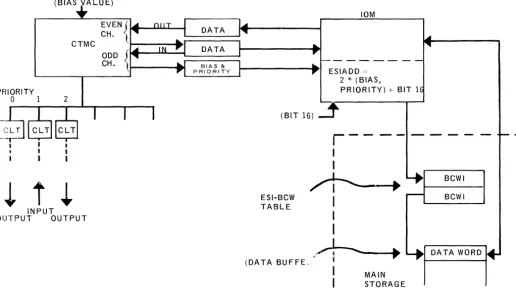
Externally Specified Indexing (ESl)
The ESI mode of I/O Channel operation is selected for a paired channel to which a Communication Terminal Module Control Subsystem (CTMC) is connected and to
UP-7627 418·111 PROCESSOR AND STORAGE 4
SECTIONI
which in turn up to 16 Communication Terminal Modules (CTM) may be added. Each CTM comprises two or four Communication Line Terminals (CL T).
When a channel is operating in the ES I mode, 18 bits are transmitted, bit-parallel, between main storage and the CTM by way of the 10M and the CTMC Subsystem. Data transmissions to or from a number of CTM's are multiplexed on one I/O channel through the operation of the CTMC subsystem.
Channels operating in ESI must be in paired channel mode. Data and external function words are transmitted on the even numbered channel of the pair. Control signal lines of the odd channel control input and output transfers. External functions are transmitted through the even channel External Function line.
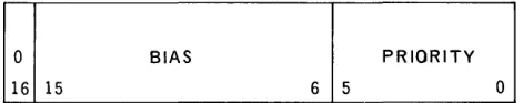
Accompanying each data transfer between the CTMC and the processor is an ESI address identifying which pair of BCW's is to be used to control the data transfer. The ES I address has the following format:
BIAS PRIORITY I
~
The low order six bits of the ES I address identify the CL T to or from which data is to be transferred. All input CL T's have odd priority codes, and all output lines have even priority codes as indicated by bit O.
The bias bits are fixed at a specific value at system installation time: they specify the high order portion of the beginning address of the Buffer Control Word (BCW) table.
PAGEl
Since each line requires two successive BCW's it is necessary for the 10M to double the value of the ESI address when referencing the Buffer Control Words.
Figure 4-2 is a schematic representation of the ES I data transmission.
UP-7627 418-111 PROCESSOR AND STORAGE
(BIAS VALUE)
CTMC
PHIORITY
o
1 2(BIT 16)
SECTION:
10M
ESIADD =
2
*
(BIAS,PRIORITY) + BIT 1
4
PAGE:
r
-I
I
BCWI
~
t
~
ESI-BCWTABLE
~
I
I
BCWI INPUT
OUTPUT OUTPUT
I
4~
(DATA BUFFE: ' j
Figure 4-2. ESt Data Transmission
MAIN STORAGE
DATA WORD
A CT M that is prepared to perform an output operation presents a request to the CTMC when the CTM is ready to receive output data. The CTMC, which continuously scans all CTM's for service requests, locks onto the interface of the CTM requesting service and stays locked until the transfer of one data word to that CTM is complete. If more than one CTM is requesting service at the same time, they are serviced according to priority.
In order to serve a CTM which has requested to output data, the the CTMC presents an ODR to the 10 M by way of the appropriate line of the odd output channel. At the same time, the CTMC presents a 15-bit ESI value (bits 14 - 0) to the 10M by way of the odd input channel of the pair.
The ESI value is left shifted (to positions 15 to 1) in the 10M to permit double SCW's. (Address bit 16 is selectable, by connection of a jumper wire in each 10M, to locate SCW's for all ESI devices on the 10M in either of the 65K segments of main storage.) The biased ES I value specifies the absolute address of the location in main storage where the SCWT associated with the particular CTM is stored.
The 10M then obtains the SCWT and SCWI from the locations in main storage specified by the biased ES I value. The 10M then obtains the output data from the location in main storage specified by the contents of the SCWl.
The data is placed on the even channel output data lines and transmitted with an Output Acknowledge (OA) signal via the CTMC to the CTM. Also, the BCWI is tested for the terminal condition, updated, and then restored in the main storage location fromwhich it was obtained. After the CTM receives the output data and OA signal, the CTMC then
UP .. 7627 418·111 PROCESSOR AND STORAGE
4.8.2.1.
4.8.2.2.
4 SECTION:
seeks another CTM to service.
A CTM that is conditioned to perform an input operation presents a request to the CTMC when it is ready to send