Linear array of InAs APDs operating at 2 µm
Ian C. Sandall,1,* Shiyong Zhang,1 and Chee Hing Tan1
1 Department of Electronic and Electrical Engineering, Sir Frederick Mappin Building, University of Sheffield,
Mappin Street, Sheffield, S1 3JD, UK.
Abstract: A linear array of avalanche photodiodes (APDs) comprising of 128 pixels was fabricated from InAs. The uniformity of the dark currents and avalanche gain was investigated at 77, 200 K and room temperature. The array shows highly uniform results apart from some defective pixels at the edge of the arrays. At 200 K and at a wavelength of 2.04 µm, we obtained an unmultiplied responsivity of 0.61 A/W at 0 V, along with a gain of 8.5 at a bias of 10 V.
2013 Optical Society of America
OCIS codes: (040.1240) Arrays; (040.6808) Thermal (uncooled) IR detectors, arrays and imaging; (040.1345) Avalanche Photodiodes; (250.0040) Detectors.
References and links
1. M. H. Ettenberg, M. A. Blessinger, M. T. O'Grady, S. Huang, R. M. Brubaker, and M. J. Cohen, “High-resolution SWIR arrays for imaging at night,” Proceedings of SPIE . 5406, 46-55 (2004). 2. I. M. Baker, S. S. Duncan, and J. W. Copley, “A low-noise laser-gated imaging system for long-range
target identification,” Proceedings of SPIE 2004. 5406, 133-144 (2004).
3. A. Krier, H. H. Gao, and Y. Mao, “A room temperature photovoltaic detector for the mid -infrared (1.8–3.4 μm) wavelength region,” Semicond. Sci. Technol. 13, 950-956 (1998).
4. Z. Zhang, Y Zhao, Y. Zhang, L. Wu, and J. Su, “A real-time noise filtering strategy for photon counting 3D imaging lidar,” Opt. Express 21, 9247-9254 (2013).
5. A. Joshi and S. Datta, “High-speed, large-area, P-i-n InGaAs photodiode linear array at 2-micron wavelength,” Proceedings of SPIE 8533, 83533-83542 (2012).
6. N. A. Bazaev, Yu. P. Masloboev, and S. V. Selishchev “Optical methods for noninvasive blood glucose monitoring,” Biomedical Engineering 45, 229-233 (2012).
7. E. Ryckeboer, A. Gassenq, M. Muneeb, N. Hattasan, S. Pathak, L. Cerutti, J.B. Rodriguez, E. Tournié, W. Bogaerts, R. Baets, and G. Roelkens “Silicon-on-insulator spectrometers with integrated GaInAsSb photodiodes for wide-band spectroscopy from 1510 to 2300 nm,” Opt. Express 21, 6101-6108 (2013). 8. Y. Shimizu, J. Ishii, Y. Kaneko, F. Sakuma, and A. Ono, “State of the arts of the infrared radiation
thermometry standards in the middle temperature range at NMIJ,” SICE Annual Conference 2004. 1803-1807 (2004).
9. A. R. J. Marshall, C. H. Tan, M. J. Steer, and J. P. R. David, “Electron dominated impact ionization and avalanche gain characteristics in InAs photodiodes,”Appl. Phys. Lett. 93, 111107 (2008). 10. A. R. J. Marshall, P. Vines, P. J. Ker, J. P. R. David, and C. H. Tan, “Avalanche multiplication and
excess noise in InAs electron avalanche photodiodes at 77 K,” IEEE J. Quantum Electron. 47, 858-864 (2011).
11. S. Ghosh, S. Mallick, K. Banerjee, C. Grein, S. Velicu, J. Zhao, D. Silversmith, J. B. Rodriguez, E. Plis, and S. Krishna “Low-noise mid-wavelength infrared avalanche photodiodes,” J.Electron. Materials 37, 1764-1769 (2008).
12. V. I. Stafeev, K. O. Boltar, I. D. Burlakov, V. M. Akimov, E. A. Klimanov, L. D. Saginov, V. N. Solyakov, N. G. Mansvetov, V. P. Ponomarenko, A. A. Timofeev, and A. M. Filachev, “Mid- and far-IR focal plane arrays based on Hg1–xCdxTe photodiodes,” Semiconductors 39, 1215–1223 (2005).
13. J. Beck, C. Wan, M. Kinch, J. Robinson, P. Mitra, R. Scritchfield, F. Ma, and J. Campbell, “The HgCdTe electron avalanche photodiode,” J. Electron. Materials 35, 1166-1173 (2006).
14. R. Sidhu, L. Zhang, N. Tan, N. Duan, J.C. Campbell, A.L. Holmes, Jr., C.-F. Hsu, and M.A. Itzler, “2.4 µm cutoff wavelength avalanche photodiode on InP substrate,” IET Electron. Lett. 42, 20063415 (2006).
15. D. S. Ong, J. S. Ng, Y. L. Goh, C. H. Tan, S. Zhang, and J. P. R. David, “InAlAs avalanche photodiode with type-II superlattice absorber for detection beyond 2 μm,” IEEE Trans. Electron. Device 58, 486-489 (2011).
16. O.V. Sulima, M.G. Mauk, Z.A. Shellenbarger, J.A. Cox, J.V. Li, P.E. Sims, S. Datta and S.B. Rafol, “Uncooled low-voltage AlGaAsSb/InGaAsSb/GaSb avalanche photodetectors,” IEE Proc.-Optoelectron. 151, 1-5 (2004).
17. S. J. Maddox, W. Sun, Z. Lu, H. P. Nair, J. C. Campbell, and S. R. Bank, “Enhanced low-noise gain from InAs avalanche photodiodes with reduced dark current and background doping,” Appl. Phys. Lett.
18. P. J. Ker, A. Marshall, A. Krysa, J. P. R. David, and C. H. Tan, “Temperature dependence of leakage current in InAs avalanche photodiodes,” IEEE J. Quantum Electron. 47, 1123–1128 (2011).
19. M. H. Woods, W. C. Johnson, and M. A. Lampert, “Use of a schottky barrier to measure impact ionization coefficients in semiconductors,” Solid State Electron. 16, 381-394 (1973).
20. P. J. Ker, A. R. J. Marshall, J. P. R. David, and C. H. Tan “Low noise high responsivity InAs electron avalanche photodiodes for infrared sensing,” Phys. Status Solidi C9 310–313 (2012)
1. Introduction
Digital imaging has until recently been dominated by Si based arrays, which are only able to detect visible or near infrared light due to the bandgap of Si. As such imaging in the short and mid wave infrared (SWIR, MWIR) regions of the spectrum has not been as intensively exploited. Imaging in the SWIR offers potential benefits such as imaging using reflected star light [1] which peaks in intensity at a wavelength of 1.7 μm, or active imaging using a pulse from an eye-safe 1.55 μm laser to illuminate a dark scene and image the reflection [2]. Imaging in the MWIR can also be used for radiation thermometry applications, such as to monitor the manufacturing temperature of plastics. In addition there are a number of imaging applications which require a detection wavelength around 2 µm including; 3D LIDAR detection for CO2 in both ground-based and airborne applications [3-5], imaging the diffusion of Glucose [6-7] and ‘cold’ radiation thermometry to identify regional hot spots [8].
Due to its bandgap InAs can respond to wavelengths from the visible up to the MWIR, which makes it highly attractive for use in this class of imaging equipment. Furthermore over recent years InAs has been demonstrated to operate as an excellent avalanche photodiode (APD) over this spectral range with single carrier multiplication and low excess noise [9-10]. Alternative semiconductor materials that could be utilized for imaging applications over this wavelength range include Cadmium Mercury Telluride (CMT) [11-12], the band gap of which can be tuned via its composition from 1 to 16 µm, with high gain and low noise. Additionally CMT APDs have been successfully demonstrated in Focal Plane Arrays [12]. However CMT is an expensive and difficult semiconductor to grow and fabricate, limiting both the price and quantity of devices that are available. CMT APDS have previously demonstrated high gains at longer wavelengths (a gain of 100 has been reported with an applied bias of 5 V when operating at 9 µm) [13]. However when the composition is changed to lower the cut-off wavelength the gain also reduces (when operating at 2.2 µm a gain of less than 2 is achieved at 5 V) [13]. GaAsSb/InGaAs Type-II superlattices have also been successfully demonstrated as photodiodes operating in the 2 – 3 µm range. Furthermore they can be operated in an avalanche mode by forming a separate-absorption-and-multiplication (SAM) APD, where the superlattice forms the absorber and InP [14] or InAlAs is used for the multiplication [15]. APDs utilizing the bulk semiconductor InGaAsSb have also been realized over this wavelength range [16], however the growth and fabrication of this material is still at a very early stage with devices dominated by large surface currents. Consequently no APD arrays have been reported from the Type II and InGaAsSb devices to date.
Most of the recent work in InAs has been focused on improving fabrication and growth techniques for mesa diodes, as evidenced by the most recent publications being on studies of leakage currents [17-18], with the best results being obtained using wet chemical etchants and photoresist based passivation. However it is not clear at present whether these fabrication techniques are robust and reliable enough to allow the realization of a uniform array which could be deployed for imaging applications.
In this paper we report on the first 128 pixel linear array of InAs APDs which have been fabricated using standard mask lithography and wet chemical etching techniques. We have investigated both the electrical and optical uniformity of the array as well determining the degree of electrical isolation between the pixels.
2. Experimental details
currents [9-10]. Therefore to ensure electron injection into the multiplication region the incident signal should be fully absorbed in the p-doped layer in a p-i-n based APD design. However for use in imaging applications using 2D arrays, the reverse structure, a n-i-p design, would be grown to allow the pixels to be bonded via a flip-chip technique for integration with the read out electronics before the substrate is removed to allow illumination on the p-layer. For this reason the structure investigated in this work is a n-i-p configuration with an n+ top layer. The structure was grown via solid source molecular beam epitaxy (MBE) on a 2-inch p+ InAs substrate at 510 Celsius with a growth rate of 0.6 ML/s. The high growth temperature used here was chosen to increase the growth rate so that impurity incorporation can be kept low [17]. In and As2 fluxes were supplied from a dual filament effusion cell and a valved cracker respectively. An As2/In beam equivalent pressure ratio of 10 was used for the whole structure. The substrate was rotated at a speed of 30 rpm to minimize the effect of heating and flux non-uniformity. The structure consists of a 1.5 µm p+ doped (1x1018 cm-3 of Be) layer followed by a 4 µm undoped layer and then a 2 µm n+ doped (1x1018 cm-3 of Si).
The pixel array was defined via standard contact mask lithography (to form square pixels with dimensions of 50 µm square) and the pixels were etched using our preferred chemical etching procedures of a 1:1:1 (phosphoric acid: hydrogen peroxide: de-ionized water) etch, followed by a finishing etch of 1:8:80 (sulphuric acid: hydrogen peroxide: de-ionized water) [9]. The diodes were then passivated with SU8, which has previously been found to suppress surface leakage currents in large area mesas down to 77 K [6]. The SU8 layer also formed a dielectric layer upon which the bond pads were deposited. The bond pads and top contacts were deposited simultaneously in the same step and were formed from Ti/Au with thicknesses of 20/200 nm. A common p contact was formed using 20/200 nm of Ti/Au. An SEM image of a section of the array is shown in Fig. 1, each pixel had a fill factor of 67%.
Fig. 1. (a) SEM image of a section of the fabricated array, (b) magnified image of pixel and bond pad and an optical image of the array
3. Results and discussion
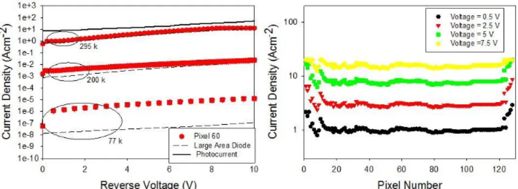
To assess the uniformity of the array we measured the IV characteristics of each individual diode in the array with the results shown in Fig. 2. Fig. 2a shows that the full IV measurements for a selected pixel (several pixels were compared but only one shown for clarity) at three temperatures. At all temperatures the IV characteristics are very similar indicating highly uniform wafer growth and fabrication processes. The IV results for a large area diode (circular mesa with a radius of 100 µm) which has been fabricated from the same wafer is also included for comparison. The current densities, for both the pixels from the array and the large area diode, are in excellent agreement at room temperature indicating that the dark currents in these diodes are dominated by bulk mechanisms. However as the temperature decreases an increasing discrepancy between the array pixels and large area diode is observed indicating the presence of surface leakage at lower temperatures.
To further investigate the uniformity of the array Fig. 2b shows the measured dark current density as a function of pixel number at a fixed bias at room temperature. From Fig. 2b it can be seen that the array has a good uniformity with the measured current, with only approximately a 5 % variation in the majority of pixels. Larger variations are observed on either end of the array (i.e. 10 pixels on each end). This increased variation in current is believed to be originating from the fabrication process due to the relatively small size of the sample. The array was fabricated on a piece of wafer with dimensions approximately 2 mm longer than the total length of the array, resulting in only a 1 mm gap between the last pixel and the edge of the wafer as shown in Fig. 1b. As such the end pixels may be degraded due to edge bead effects, cleave planes and physical sample handling.
Fig. 2. (a) IV characteristics of a selected pixel (symbols) and a reference large area mesa (dashed lines) at temperatures of 295, 200 and 77 K, the 295 K photocurrent is also plotted
(solid line), (b) dark current as a function of pixel number at fixed voltages.
Fig. 3. Current as a function of pixel number for selected voltages at 200 (a) and 77 K (b).
From Fig. 3 it can be seen that at both temperatures the array still has a high uniformity with an increased variation in current, again only occurring at the edges.
Having established that we have fabricated a uniform array we evaluated its performance as an array of APDs. For these measurements we have measured the avalanche gain of each pixel in the array at a wavelength of 2.04 µm at a temperature of 200 K by coupling the laser emission into a fiber and focusing it onto each pixel. Since the wafer structure is an n-i-p configuration but we require electron injection to initiate impact ionization in InAs [9] the laser emission from the fiber (with core diameter 62.5 µm) was shone onto the p+ layer, at the bottom floor, of each pixel to achieve predominantly pure electron injection. Due to practical limitations concerning the sample and experimental set up, this method of performing the analysis of the array may have some mixed injection which could lower the gain at a given bias. The photocurrent was measured under a DC technique where the total current (dark and photocurrent) was measured via an SMU.
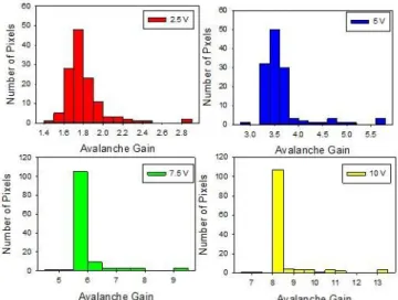
The measured avalanche gain at 200 K is shown in Fig. 4, where Fig. 4a shows the gain curves for selected pixels while Fig. 4b shows the gain at a fixed bias as a function of pixel number. The gain curves observed are typical for InAs due to impact ionization being initiated only by electrons [9] where the onset of gain is observed at very low voltages and the gain rises exponentially with voltage. The gain curves for all of the pixels show a high level of agreement (as illustrated with the selected pixels in Fig. 4a) illustrating that the sensitivity of the gain is the same for all pixels. At zero bias, the measured photocurrent results in a calculated responsivity of 0.6 A/W.
Fig. 4. (a) DC gain characteristics of selected pixels (symbols) and gain determined using phase-sensitive detection (dashed lines), (b) gain as a function of pixel number at fixed
voltages all performed at 200 K.
Fig. 5. Histogram distributions of avalanche gain at selected voltages. Measurements were performed at 200 K.
Using a DC measurement technique for the determination of the avalanche gain can introduce errors when the ratio of photocurrent to dark current is small. From Fig. 2a it can be seen that at room temperature the ratio of photocurrent to dark current is approximately 10 at 0 V. However the ratio decreases slightly as the voltage is increased. As the dark current decreases with decreasing temperature while the photocurrent remains approximately constant this ratio will increase at lower temperatures. To verify that errors have not been introduced into our measurements from this technique we have re-measured the gain of the same selected pixels as shown in Fig. 4a using a phase-sensitive detection approach (lines in Fig. 4a). Due to the nature of our experimental set up which requires each individual pixel to be manually probed and aligned it was not feasible to test the whole array under these conditions. However the selected pixels show an excellent agreement between the two methods, illustrating that our DC method has not lead to significant errors as the photocurrent to dark current ratio is relatively large (for example a ratio of 31 is obtained at 0.5 V at 200 K). Our measurements confirm that under DC method the gain appears to be higher for the pixels near the edges, but phase sensitive measurements show a lower gain which is consistent with that obtained from the center of the array. The reason for these discrepancies is believed to be the increased dark current at the edge which reduced the signal to noise leading to measurement errors, when DC method is used.
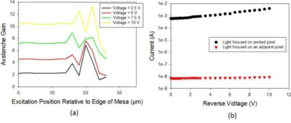
relative to a fixed laser spot of 10 m. The initial position is taken as the edge of the pixel as viewed from directly above; the device is then moved linearly away from this point. The measured gain as a function of excitation position, using phase sensitive detection is shown in Fig. 6a. It can be seen that significant error in gain was measured when the optical spot is more than 15 m away from the pixel. Inferring from this, we believe that our fiber alignment during gain measurements in Fig. 4 is within 15 µm from the pixel since highly uniform gain was measured.
Fig. 6. (a) Room temperature avalanche gain as a function of excitation position (b) Measured photocurrent when light is focused onto a probed pixel (circles) and when
focused onto an adjacent pixel (triangles).
To evaluate how well isolated the individual pixels are, we have measured the photocurrent from a pixel while focusing the incident radiation on an adjacent pixel. This measurement was again performed at room temperature using the same laser but with free space optics to ensure an optical spot smaller than the pixel. The measured photocurrent responses when the light was focused onto the measured pixel and an adjacent pixel are shown in Fig. 6b. An approximately voltage independent photocurrent of less than 10 nA was recorded which is over five orders of magnitude lower than the directly measured photocurrent is observed. This indicates that the individual pixels have a good degree of optical isolation and that the small measured photocurrent is thought to be most likely due to stray reflected light.
4. Conclusion
In summary we have fabricated and tested a linear array of InAs APDs with 128 pixels. We have observed good uniformity in the dark currents at all temperatures and a highly uniform gain distribution at 200 K under excitation at 2 µm. These results suggest that InAs is a highly promising material to from infra-red imaging arrays in the future.
Acknowledgments