Performance Analysis of 1-bit Full Adder with
Optimized Leakage Power using Cadence
180nm & 90nm Technology
Shraddha Melinamani 1, Silpa Ajith Kumar 2
P.G. Student, Department of E&IE, Dayananda Sagar College of Engineering, Bengaluru, India1
Assistant Professor, Department of E&IE, Dayananda Sagar College of Engineering, Bengaluru, India2
ABSTRACT: Full adder is the key component for most of the VLSI design system. Some of its applications include ADC, Wallace Tree Encoder, and Arithmetic Logic Unit and many more. The growth of VLSI system is aiming at low power, low area and high speed design. Low power design circuits play a versatile role in any VLSI design of current growing technologies. Leakage power is the main component of power dissipation. Power dissipation is inversely proportional to the battery life. As the power dissipation decreases battery life of portable device increases. In this paper, we have proposed a new architecture for low power full adder circuit. The proposed architecture of full adder is divided into four sections for the analysis purpose. The architecture analysis is accomplished in 3 cases. Proposed full adder gives less leakage power in all three cases compared with conventional adder. The design has been carried out in 180NM Technology and 90nm Technology using Cadence Virtuoso analog environment.
KEYWORDS:Full adder, Leakage power, CMOS circuits, Leakage current, Static power dissipation, Performance.
I. INTRODUCTION
In VLSI design the integration of number of transistors on single chip reduces the cost and improves the design. In earlier days the integrated chips were limited to some functionalities. According to the Moore’s law the number of transistors are increasing to billions on a single chip. Due to the factor of scaling and chip size reducing, the power dissipation is increasing which leads to heat the integrated chip and damages it. Power dissipation is mainly caused by static power dissipation and dynamic power dissipation and short circuit power.
Static power dissipation occurs when the circuit is in inactive state i.e no operation condition. It is also defined as the product of supply voltage and leakage current[7]. It is represented as shown in equation (1).
Is=I0[ -1] (1)
Is=saturation current, K=Boltzmann’s constant, V=diode voltage, T=temperature Total static power dissipation is given by
Pstatic=Σ Is. Vdd (2)
Dynamic power dissipation occurs when transition takes place at the output i.e in conduction state of circuit. It is given as shown in equation (3)
Pdynamic=CL. Vdd2. f (3)
CL=load capacitance, f=operating frequency, Vdd=supply voltage
Short circuit power occurs when both PMOS and NMOS transistors are on at the short time periods, hence occurs path from Vdd to Vss. It can be equated as
In this work Full adder is proposed as it is the basic circuit for all digital systems. By reducing size and cost the system reliability can be increased in chip design. The area and power consumption are depend upon the hardware size. But technology is concentrating for long battery life and small size with better functionality.. In order to get the long battery life the power dissipation is main constraint[6].
Paper is organized as follows. Section II talks about literature survey on previous works. The basic block diagram of 1-bit full adder is divided into four sections, and the proposed technique is applied for full adder in three different cases that is given in Section III. Section IV describes experimental results showing schematics of conventional and proposed full adder circuit and the comparison results of leakage power in 90NM and 180NM technology using Cadence. Finally, Section V concludes the work.
II. RELATEDWORK
This section provides the different design techniques used for leakage current minimization.
1. In Multi Threshold voltage CMOS(MTCMOS) technique the logic implementation can be done by low threshold voltage transistors and high threshold voltage transistor acts as sleep transistor, which are used on the non-critical path to reduce the leakage current[4].
2. In power gating technique by cutting off the supply voltage the device turns off. It includes extra sleep transistors which can be placed in between pull up network & supply voltage and pull down network & ground in order to reduce the standby leakage current[2][3].
3. In drain gating technique sleep transistors are placed between pull down and pull up networks for reduction of leakage current. To reduce the resistance of conducting path sleep transistors are turned on during active mode and hence the performance degradation is reduced. In standby mode sleep transistors are turned off and the resistance path from supply to ground increases by producing high resistance path[5].
4. In sub threshold logic technique, the supply voltage is scaled at very low level. This method reduces leakage power and has the limitation of very slow speed[6].
III. PROPOSEDTECHNIQUE
A. Full Adder Design
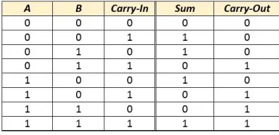
Full adder performs with 3 bit binary inputs and gives two 1 bit binary outputs. The truth table of full adder is shown in the table 1. A,B,C are the binary inputs and sum, carry are the outputs. The expression for sum and carry are given as below.
Sum= A^B^ C (5) Carry= AB|BC|AC (6)
Table 1: Truth table of 1-bit full adder
Fig 1. Conventional 28T CMOS 1-bit full adder
Conventional full adder circuit is divided into four blocks as shown in the above figure for easy analysis of results.
Fig 2. Block diagram of conventional adder
Basic block diagram of full adder is divided into four different blocks as shown in figure 2 for different and easy analysis with different cases.
B. Technique
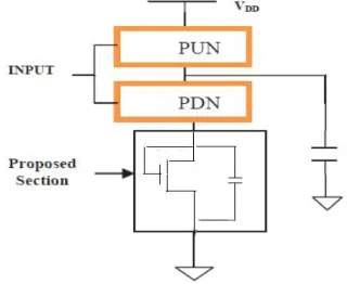
In this paper “stacking effect” has been introduced for reduction of leakage current. Leakage power always flow in low resistance path whenever the circuit is in standby mode. In this technique extra transistor is placed in between the pull down network and ground as it is the low resistance path.
The block diagram of proposed technique is as shown in the above figure 3. One transistor is placed across capacitor in between ground and pull down network. Here low Vth NMOS transistors are used so as to get the full swing output voltage. The gate terminal of this NMOS transistor is connected to the drain terminal of its own, hence it generates self ON-OFF condition. One capacitor is added in between the pull down network and ground across the NMOS transistor to block the static leakage current because of the high reactance property of capacitor to DC signal. The capacitor gets charged up to Vdd, once it gets fully charged it will remain at the same state as there is no discharge path and hence blocks the static leakage current.
I. Case A:
Fig 4. First attempt for full adder
As shown in the figure 4, all four blocks are grouped together and connected to a proposed circuit hence the delay time will increase and power consumption is reduced as we have used less number of transistors.
II. Case B:
Fig 5. Second attempt for full adder
As shown in the figure 5, each two-two blocks are grouped together and connected to proposed circuits respectively hence the delay time will be minimized and power consumption will increase as compared to the Case A. as we have increased the number of transistors in the proposed section.
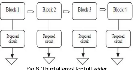
III. Case C:
As shown in the figure 6, each individual blocks are connected to one-one proposed circuits respectively hence the delay time will be decreased and power consumption will be increased as we have increased the number of transistors in the proposed section.
IV. EXPERIMENTAL RESULTS
The figure 7. is the schematic diagram for the conventional full adder circuit. It is simulated in the both 180nm and 90nm technologies using Cadence Virtuoso. It is designed with NAND and NOR gates as these are the universal gates for all designs.
Fig 7. Schematic of conventional 1-bit full adder
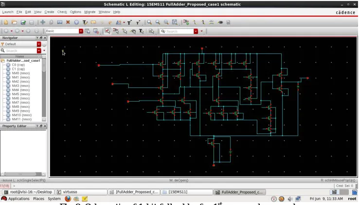
The figure 8. is the schematic diagram for the proposed section of full adder circuit which is shown in the Case A. It is simulated in the both 180nm and 90nm technologies Cadence Virtuoso. The proposed section is added to the all four sections parallel. It consumes less area compared to other two cases as the number of transistors are less.
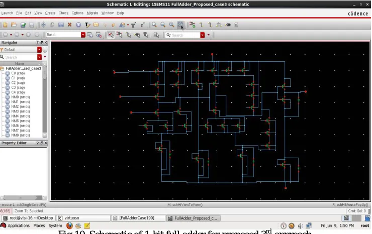
The figure 9. is the schematic diagram for the proposed section of full adder circuit which is shown in the Case B. It is simulated in the both 180nm and 90nm technologies Cadence Virtuoso. Proposed section is added to first two sections and second two sections of full adder. This circuit performs speed as compared to the first case.
Fig 9. Schematic of 1-bit full adder for proposed 2nd approach
The figure 10. is the schematic diagram for the proposed section of full adder circuit which is shown in the Case C. It is simulated in the both 180nm and 90nm technologies Cadence Virtuoso. Proposed section is added to all four sections of full adder circuit. Area will increase as the number of transistors are increased compared with previous cases.
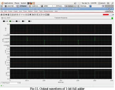
The below figure 11. shows the output of the full adder circuit which is simulated in the both 180nm and 90nm technologies Cadence Virtuoso. Here A,B and Cin are the inputs and Sum and Cout are the outputs. When A=0, B=0, C=0 then Sum and Carry outputs are 0. If A=1, B=1, C=1 then Sum and Carry outputs are 1. And outputs are verified with all other combinations of inputs according to the truth table of full adder.
Fig 11. Output waveform of 1-bit full adder
Table 2 gives the information of comparative results of leakage power in both 180nm and 90nm CMOS technologies. According to table it is clear that all three proposed sections gives less leakage power compared with conventional adder. As the technology grows the power dissipation increases. In 180nm the static power dissipation is in terms of Pico watts but in 90nm technology static power dissipation is in terms of Nano watts.
Table 2: Comparative Results of Leakage Power
Case Study Leakage Power
180nm Technology 90nm Technology
V. CONCLUSION
In this paper stacking method for 1-bit full adder is proposed with optimal leakage power consideration. Implementing the proposed design is done using Cadence virtuoso analog environment with 180nm and 90nm technologies. Supply voltage of Vdd=1.8V is used for 180nm technology and Vdd=1V for 90nm technology. Full adder is sectioned with four blocks and the proposed technique is applied to all the four with different cases. Leakage power is reduced in all three proposed sections compared with conventional circuit in both 180nm and 90nm technologies. In future work this implementation can be done in 45nm technology and used in the applications like DSP applications, Arithmetic logic unit, Wallace tree encoder, Flash analogue to digital converter etc.
REFERENCES
[1] Prasenjit Deb, Alak Majumder, “Leakage Reduction Methodology of 1-bit Full Adder in 180nm CMOS Technology”, IEEE Third International Conference on Devices, Circuits and Systems, pp. 199-203, 2016.
[2] M. D. Powell, S.-H. Yang, B. Falsafi, K. Roy, and T. N. Vijaykumar,“ Gated-Vdd: A circuit technique to reduce leakage in deep submicron cache memories,” in Proc. IEEE ISLPED, pp. 90-95, 2000.
[3] Z. Chen, M. Johnson, L. Wei and K. Roy, “Estimation of standby leakage power in CMOS circuit considering accurate modeling of transistor stacks,” in Proc. IEEE ISLPED, pp. 239-244, Aug. 1998.
[4] S. Mutoh, T. Douseki, Y. Matsuya, T. Aoki, S. Shigematsu, and J. Yamada, “1-V power supply high-speed digital circuit technology with Multi-threshold voltage CMOS,” IEEE J. Solid-State Circuits, vol. 30, pp. 847–854, Aug. 1995
[5] Bipin Gupta, Sangeeta Nakhate, “Transistor Gating: A Technique for Leakage Power Reduction in CMOS Technology”, International Journal of Emerging Technology and Advanced Engineering, volume 2, Issue 4, pp. 321-326, April 2012.
[6] Ajeet Thakur, Rajesh Mehra, “Power and Speed Efficient Ripple Counter Design using 45nm Technology”, 1st IEEE International Conference on Power Electronics, Intelligent control and Energy systems, pp. 1-4, 2016.
[7] A. Kumar, S. Kumar, R.Das, “Area-Delay-Power Efficient PSO based Full Adder in Different Technologies ”, IEEE International Conference on Communication and Signal Processing, pp. 1762-1766, April, 2016.
[8] Saradindu Panda, A.Banerjee, B.Maji, Dr.A.K.Mukhopadhyay, ”Power and Delay Comparison in between Different types of Full Adder Circuits ”,Inter national Journal of Advanced Research in Electrical, Electronics and Instrumentation Engineering, ISSN: 2278 – 8875 [9] P. Landman and J. Rabaey, “Architectural power analysis: The dual-bit type model,” IEEE Trans. VLSI Syst., vol. 3, pp. 173– 187, Feb. 1995. [10] Partha Bhattacharyya, Bijoy Kundu, Sovan Ghosh, Vinay Kumar, Anup Dandapat, “Performance Analysis of a Low-Power High-Speed