ABSTRACT
AKOUALA, CHRISTER RAJIV. Planar Hall Effect in Magnetic Conducting Oxides. (Under the direction of Dr. Frank Hunte).
Planar Hall Effect in Magnetic Conducting Oxides
by
Christer Rajiv Akouala
A dissertation submitted to the Graduate Faculty of North Carolina State University
in partial fulfillment of the requirements for the degree of
Doctor of Philosophy
Materials Science and Engineering
Raleigh, North Carolina 2015
APPROVED BY:
_______________________________ _______________________________
Dr. Frank Hunte Dr. C. Lewis Reynolds Jr.
Committee Chair
_______________________________ _______________________________
DEDICATION
BIOGRAPHY
I was born in Brazzaville (Republic of Congo) on November 19th 1988, the fifth child of Fulbert and Suzanne Akouala. My siblings include Elvire, Sidney, and the twins Davina and Jerry. We all lived in Brazzaville until we moved to Washington DC in 2001 when I was 12 years old. I attended high school at the Kamit Institute for Magnificent Achievers (KIMA) Public Charter School with my twin siblings. With the wonderful guidance of Ur Aua Hehimetu, the late Mrs. Myers and other great teachers, I graduated high school in 2004. From there I went on to college: first at Winston-Salem State University, studying Chemistry, then later I transferred to Appalachian State University, where I studied and graduated with a degree in Applied Physics in 2009. A year before graduating, I attended a summer research program at the University of Michigan, with Prof. Goldman’s group. I investigated the effects of annealing on the electronic properties of GaAsN. This research was my introduction to the multidisciplinary approach of Materials Science and Engineering (MSE). In this field I found a way to bring together my interests in chemistry, physics, and engineering. This is when I decided that MSE would be the subject of my graduate degree.
I was admitted and started working on my doctorate in MSE at North Carolina State University in 2010. Between 2010 and 2012, I completed my coursework, passed my qualifier, and got some research experience working with thin films growth and characterization. In 2013, I joined the Hunte advanced magnetics materials research group, and went on to finish my PhD.
Ross Ledford). I had my world shattered and pieced back together many times, and am now (hopefully) more prepared to face the world and its uncertainties. Look out.
ACKNOWLEDGMENTS
I am very grateful for the support, guidance, and encouragement of my advisor, Prof. Frank Hunte. Thanks Dr. Hunte for your mentorship, for helping me to build confidence in myself and to find my own work-life balance. I also thank all my committee members: Professors Lew Reynolds, Jay Narayan, and Dan Dougherty for challenging me to do my best work.
Many thanks to my research group members: Raj Kumar, for being a great mentor since day zero in the group, Sandhyarani Punugupati, for providing me with PLD grown ZnO samples and for her input and reality checks, and Chris Ledford, for all his help in many ways, both in the lab and outside of lab (thanks for the gym exercises, car fixes, free meals, life advice, and so much more).
Many thanks to my collaborators: Drs. Lew and Judy Reynolds for providing me with MOVPE grown ZnO samples, Yvonne (Yi-Fang) Lee for providing me with PLD grown SnO2 samples, Edward Sachet(and Prof. Maria) for providing me with CdO samples, Dr. Srinavasa Rao for providing me with LSMO samples for preliminary testing, and Edward Mily for the CuO samples.
a “care” so much for what people think, and more), and Andreas Hoffie (for the awesome lunches/discussions we shared and the honor of being one of his groomsman).
I give a special thanks to Ms. Edna Deas for all her help throughout my entire graduate school experience.
I also thank the entire MSE office staff for all their assistance with technical and administrative matters: Toby Tung, Joe Matthews, Wade Myers, Mary Ann, Paola, Meghan, Elaine, Kara, Liz, Jan, and Warren.
Thanks to my neighbors: Ms. Laura, for your incredible presence in my life, you helped me get my first car, you shared meals with me, listened to my stories and gave me great advice. Thanks for being part of my family away from home. Mr. Ali, for always sharing life advice with me, feeding me, and treating me like a son.
Thanks to the twins, Jennifer and Joanna, for their friendship and especially for giving me a ride to Raleigh for my grad school interview. I did it! I finished the adventure that you helped me to start.
Thanks to Marc Hunt for being a great friend and for introducing me to the Raleigh’s adult soccer league. Thanks to my LFC, Zodiac, and MSE Titans teammates for the fun times. Thanks Terran Berry and EC Old Boys for the weekend soccer tournaments. Soccer has always helped to keep me balanced in school, too little or too much of it was detrimental to my life balance.
Thanks to Peter Peyechu and my FC Bondeko team. Thanks also to my former pastors for their encouragement and helping me towards realizing my potential: Pastors Jules (and Mama Anne-Marie), Mulumba Kalala, Shisso Israel, and Hygin Ntondo.
TABLE OF CONTENTS
LIST OF TABLES ...x
LIST OF FIGURES ... xi
CHAPTER 1: PHE AND AMR ...1
1.1 Introduction ...1
1.2 Motivation (scientific objective)...2
1.3 Planar Hall Effect ...3
CHAPTER 2: MAGNETIC SEMICONDUCTORS ...7
2.1 Magnetism in materials ...7
2.2 Electrical conduction in materials ...9
2.3 Ferromagnetism in Semiconductors ...11
2.4 Background of material systems (Materials Background) ...11
2.4.1 ZnO ...12
2.4.2 SnO2 ...14
2.4.3 CdO ...15
2.4.4 CuO ...15
2.5 Theories of unexpected ferromagnetism in semiconductor ...16
CHAPTER 3: EXPERIMENTS ...18
3.1 Sample preparation techniques ...18
3.2 Magnetoresistance and Hall effect ...19
3.3 Magnetometry ...19
3.4 PHE and AMR ...20
CHAPTER 4 - DATA & ANALYSIS ...21
4.1 Transport & Magnetism of Undoped & Cobalt Doped ZnO thin film ...21
4.2 PHE in Cobalt Doped ZnO ...31
4.3 PHE in Undoped ZnO thin films grown by MOVPE and PLD ...34
4.4 Effects of Annealing on ZnO Magnetotransport Properties ...50
4.5 PHE in SnO2 ...60
4.6 PHE in CdO ...69
4.7 PHE in CuO ...82
CHAPTER 5: CONCLUSIONS ...89
CHAPTER 6: FUTURE WORKS ...93
REFERENCES ...94
APPENDICES ...102
APPENDIX A: ADDITIONAL MR OF PLD SAMPLES ...103
APPENDIX B: TEMPERATURE DEPENDENT PHE AND AMR ...104
LIST OF TABLES
LIST OF FIGURES
Figure 1.3.1: Geometry of PHE/AMR measurements ...3
Figure 2.1.1: Magnetization graphs for paramagnets and diamagnets ...7
Figure 2.1.2: Magnetization curves for ferri- and ferromagnets ...8
Figure 2.1.3: Magnetization vs. temperature of strong ferromagnet LSMO with Tc~350 K ...9
Figure 4.1.1: θ-2θ XRD scans of (a) cobalt doped and (b) undoped ZnO ...25
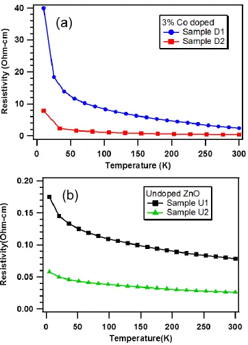
Figure 4.1.2: Resistivity vs temperature of (a) cobalt doped and (b) undoped ZnO ...26
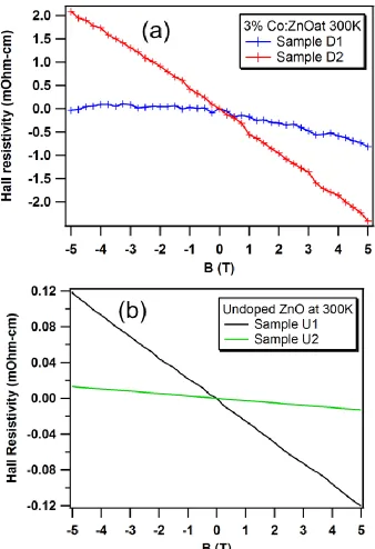
Figure 4.1.3: Hall effect vs. magnetic field of (a) cobalt doped and (b) undoped ZnO...27
Figure 4.1.4: Temperature dependence of magnetization vs magnetic field for (a) cobalt doped and (b) undoped ZnO ...28
Figure 4.1.5: Temperature dependence of magnetoresistance vs magnetic field for for (a) cobalt doped and (b) undoped ZnO ...29
Figure 4.1.6: Temperature dependence of carrier concentration and saturation magnetization for (a) cobalt doped and (b) undoped ZnO ...30
Figure 4.2.1: Temperature dependence of (a) PHE vs angle and (b) AMR vs angle for D1 cobalt doped ZnO ...32
Figure 4.2.2: Temperature dependence of (a) PHE vs angle and (b) AMR vs angle for D2 cobalt doped ZnO ...33
Figure 4.3.1: X-ray diffraction θ-2θ scans of MOVPE (a) and PLD (b) thin films ...42
Figure 4.7.1: (a) Hall effect and (b) resistivity vs. temperature for 50 nm CuO ...84 Figure 4.7.2: Temperature dependence of magnetization vs. magnetic field for (a) sample 1 and (b) sample 2 ...85 Figure 4.7.3: Temperature dependence of (a) PHE vs. angle and (b) AMR vs. angle for sample 1 ...86 Figure 4.7.4: Temperature dependence of (a) PHE vs. angle and (b) AMR vs. angle for sample 2 ...87
CHAPTER 1: PHE and AMR 1.1 Introduction
In 2003, the giant planar Hall (GPHE) effect was projected as the next major technological advance in magnetic memory beyond the highly successful applications of giant magnetoresistance (GMR). GPHE failed to deliver on its promise at that time because GaMnAs ferromagnetic semiconductors, in which it was demonstrated [1, 2], had a low Curie temperature of 45 K which rendered it impractical for applications. A decade later, based on lessons learned from the Zener, Mean Field Approach and Dietl models, several ferromagnetic semiconductors were identified which were predicted to maintain ferromagnetism at or near room temperature [3-8]. This presented an opportunity to revisit the GPHE, which was thought to be universal to magnetic semiconductors at this time. Ferromagnetic conducting oxides are systems in which both charge and spin transport can potentially be utilized in a single device. The influence of a magnetic field on both transport mechanisms can be probed and used as a mechanism for sensing and data storage.
1.2 Motivation (scientific objective)
The overarching experimental research goal of this project was to demonstrate and understand the origin and mechanism of the planar Hall effect (PHE) at room temperature in
defect-engineered metal oxide magnetic semiconducting thin films. Since high-Curie
temperature ferromagnetism was predicted to be achievable in transition metal-doped ZnO [9], the hypothesis which drove this research was that the giant planar Hall effect could be demonstrated at room temperature in defect-engineered ferromagnetic conducting oxides. This study helped to elucidate the specific material conditions (of processing, structure and properties) under which the planar Hall effect could be observed at room temperature. There were two main pathways towards achieving the right conditions for the PHE studies:
1. Controlling the growth environment to achieve oxygen or metal cation vacancies, which then made the sample semiconducting and magnetic (undoped samples).
2. Doping with magnetic ions in addition to careful control of the growth environment (doped samples).
1.3 Planar Hall Effect
In ferromagnetic conductors, the magnetoresistance is anisotropic due to the asymmetric scattering of conduction electrons. The planar Hall effect (PHE) is the transversal manifestation of this planar resistivity anisotropy. PHE is a misnomer since its origin is different from the normal Hall effect. The conventional Hall effect is due to the Lorentz force on conduction electrons which generates a transverse (Hall) voltage across a conducting material and normal to the applied magnetic field. The origin of the PHE is attributed to the interaction between magnetization and current in the plane of the film. As a consequence, the resistivity in magnetic conductors is very dependent on the direction of the magnetization with respect to the current flow. In fact, the anisotropic magnetoresistance (AMR) and the planar Hall effect can be described as the longitudinal and transverse components of the anisotropic resistivity [10]. They are described by their characteristic dependence on the angle between magnetization and current (as shown in Fig. 1), which can be described by the equations below for the AMR and PHE resistivities.
Figure 1.3.1: Geometry of PHE/AMR measurements
For the current parallel to the magnetization, resistivity has a value of ρ//, and ρ┴ for the
perpendicular case.
Both PHE and AMR have their origins in the dependence of the resistivity on the orientation of the magnetization. Spin dependent transport then gives rise to different scattering when changing the angle between magnetization and electric current direction. Although the exact parameters underlying anisotropic magnetoresistance are not yet fully understood, three microscopic theories [11, 12] have contributed to further understanding the resistivity anisotropy in ferromagnetic materials: 1) Mott’s two current model, 2) Smit’s addition of spin-orbit coupling and 3) Potter’s model with exchange splitting of energy bands.
If s-d interband scattering is the dominant feature of transition-metal electronic conductivity, then the resistivity anisotropy in ferromagnetic conductors must be due to an anisotropic scattering mechanism. Smit, therefore, proposed that an isotropic scattering potential with lower-than-cubic-symmetry-wavefunctions, due to spin-orbit interaction, could be responsible for the resistivity anisotropy in ferromagnets [11, 12]. Spin-orbit interaction also makes a magnetization (i.e. spin) direction dependent contribution to the energy of the d states. This explains magnetocrystalline anisotropy, which means that magnetization direction is more favorable in certain crystallographic directions. Therefore the d electron spin is coupled both to its orbital motion, which is then coupled to the lattice by the crystalline field. The spin-orbit interaction (Hspin-orbit=KL∙S; K is the spin-orbit coupling parameter) is treated as a small perturbation which results in a mix of states with parallel and antiparallel spins. Unoccupied parallel d states are always present but these holes are unequally distributed over the five possible d orbits; there is, however, a deficiency of hole-orbits when electrons move perpendicular to the magnetization. The transition of an s electron to a d state, under the influence of a perturbing potential, is less likely if the s electrons moves perpendicular to the plane of the orbit (i.e. parallel to the magnetization since there are few hole-orbits in this direction). Therefore, it follows that the s electrons are more easily trapped when moving parallel to the magnetization rather than in a perpendicular direction. This leads to the expected conclusion that in ferromagnetic conductors the anisotropy constant Δρ is positive, i.e. ρ// >ρ┴.
Smit’s model is that Potter’s model assumed that the d bands were uniformly exchange split with some energy separations. Potter’s model is very useful because it suggests that the ratio of K, spin-orbit coupling parameter, to the splitting energy of the two uppermost d bands is important for the production of a large anisotropy constant. This would be useful in determining which materials would likely lead to PHE/AMR at room temperature to be used in future devices.
CHAPTER 2: Magnetic Semiconductors 2.1 Magnetism in materials
It can be said that there exist three main types of magnetic materials; others fall within these three main categories. Magnetic materials are defined by their response to an applied magnetic field and their dependence on temperature. All elements on the periodic table can display the diamagnetic effect, but generally it is so small that other effects are more dominant. The diamagnetic effect is due to the induced currents within a material when a magnetic field is applied. According to Lenz’s law, these currents induce a magnetic response which is opposite to the applied field. In diamagnetic materials, there are no permanent magnetic moments, only induced moments which generate a weak and negative magnetic response. The second type of magnetic materials is a paramagnet. In these atoms, there are permanent magnetic moments present, but they are considered isolated and non-interacting. When a magnetic field is applied, their response is to align with the direction of the applied field. Therefore the response in paramagnets is weak but positive. Diamagnets and paramagnets can be illustrated by the graphs of their magnetization (M) vs. applied magnetic field (H), the slope of which is called the susceptibility (χ).
0.3
M (emu/cm3)
Paramagnet
Diamagnet
A negative susceptibility indicates a diamagnetic response and a positive susceptibility indicates a paramagnet (Fig. 2.1.1). In general, the susceptibility of diamagnets has no explicit temperature dependence. However, the susceptibility of paramagnets is in many cases inversely proportional to the temperature, although there are metallic paramagnets, called Pauli paramagnets, for which the susceptibility is independent of temperature. Because they do not possess permanent magnetic moments, most paramagnets and diamagnets are not widely used in applications. A special case of diamagnets where χ is exactly equal to -1 are superconductors.
Figure 2.1.2: Magnetization curves for ferri- and ferromagnets.
By far the most useful and applicable of magnetic materials are ferromagnets. Ferromagnets are similar to paramagnets, since they also possess permanent moments. In the case of ferromagnets, however, the moments are strongly interacting. This strong interaction results in a very large and positive response when even a small magnetic field is applied. The existence of multiple regions with different magnetization directions, domains, causes the M vs. H behavior to be non-linear (Fig. 2.1.2). Even after the magnetic field is removed, a
M (emu/cm3)
H (Oe) 500
Ferromagnet
ferromagnet can retain some remnant magnetization. Since ferromagnets are non-linear magnetic materials they cannot be easily described by the susceptibility. Instead, an important characteristic of ferromagnets is their Curie temperature. This is the temperature below which a material is said to be ferromagnetic, and above which it transforms into a paramagnet. In the ferromagnetic phase, the magnetic moments interact strongly, but above the Curie temperature, there is enough thermal energy to disturb the interaction and make the material paramagnetic.
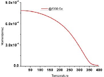
Figure 2.1.3: Magnetization vs. temperature of strong ferromagnet LSMO with Tc~350 K. (Courtesy of Raj Kumar)
2.2 Electrical conduction in materials
Resistance is the degree to which the material opposes the passage of that electric current. Ohm’s law can also be written, as in eq. 4, to relate directly to a material property which is independent of the sample geometry.
( ) (4)
(5)
(6)
The conductivity σ is the proportionality constant between the electric field generated in the material and the current density. Most commonly the resistivity ρ, which is related to the resistance (eq. 7) and the inverse to conductivity, is used to specify the electrical character of a material. In eq. 7, A is the cross-sectional area through which the current flows and d is the distance between the points where voltage is applied.
(7)
Metals, such as copper and gold are considered good conductors and have resistivities on the order of 10-5 Ohm-cm. At the other extreme are insulators, such as glass and rubber, which have large resistivity values on the order of 1010 Ohm-cm and greater. Semiconductors, like Si and Ge, have intermediate resistivities ranging from 10-2 Ohm-cm to 108 Ohm-cm. These values originate from Ref [17].
probability of some electrons scattering from the valence band to the conduction band. Insulators can be referred to as semiconductors with large energy gap (~5.5 eV as in diamond) and there are no electrons in the conduction band. There is temperature dependence to the conductivity in metals and semiconductors. There is an increase in conductivity for metal as temperature decreases, whereas for semiconductors, the conductivity increases with increasing temperature. Semiconductors are at the center of the technological advances of the 21st century. Most electronic devices that make use of transistors are made of multiple semiconducting materials. The reason why semiconductors are so useful is because their conductivity can be tuned through doping with impurity atoms.
2.3 Ferromagnetism in Semiconductors
Putting together magnetic properties and the tunable electrical properties of
semiconductors opens up the prospects of spintronic devices, where the spin and charge of electrons are both utilized. A material that exhibits both ferromagnetic and semiconductor properties at room temperature offers the prospect of combining nonvolatile magnetic storage and conventional semiconductor electronics in a single device.
2.4 Background of materials systems
2.4.1 ZnO
ZnO is a wide band gap semiconductor (~3.3 eV at room temperature) and is potentially well suited for electronic applications [18]. Doping ZnO with magnetic transition metal ions was predicted to yield room temperature ferromagnetism in p-type conducing Mn-doped ZnO [9]. Due to native defects, such as oxygen vacancies or zinc interstitials, ZnO is intrinsically an n-type semiconductor [19, 20]. The room temperature electron Hall mobility in ZnO single crystal should be on the order of 200 cm2/V·s [17]. ZnO normally crystallizes in the hexagonal (wurtzite) structure, with lattice parameters a = 3.25 Å and c = 5.12 Å. Each Zn atom is tetrahedrally bonded to four O atoms, where the Zn d-electrons hybridize with the O p-electrons [21]. The structure contains alternating layers of zinc atoms with layers of oxygen atoms. Electron doping in nominally undoped ZnO has been attributed to Zn interstitials, oxygen vacancies, or hydrogen impurities [17]. The intrinsic defect levels that lead to n-type doping lie approximately 0.05 eV below the conduction band [17]. There have been a number of studies on the preparation of ZnO thin films deposition by various methods, including metalorganic chemical vapor deposition (MOCVD) [22], variations of molecular beam epitaxy (MBE) [8, 23, 24], reactive sputtering, ion implantation, and pulsed laser deposition (PLD) [19, 20, 25-27]. PLD is the most commonly used to produce ferromagnetic films and was one of the methods used in this study.
well as doping with magnetic ions including Fe, Ni, Co, and Mn. Further, the magnetic characteristics of ZnO can be switched from diamagnetic to ferromagnetic in a reproducible manner by laser irradiation [30] and vacuum annealing [31]. Other attractive properties of ZnO include the band gap of 3.3 eV which is similar in magnitude to TiO2 while the electron mobility is an order of magnitude higher at 200 cm2V-1 s-1. Ferromagnetic ZnO also has a Curie temperature above 300K, which can be advantageous for room temperature device operation involving magnetic degrees of freedom. This is what led to the consideration of ZnO as a candidate material for the investigation of the planar Hall effect at room temperature.
Much work has been done on transition metal oxide-based thin film heterostructures which are related to room temperature ferromagnetism particularly in zinc oxide however the origin of RTFM in magnetic ion-doped ZnO is still under debate. The focus has been on the origin of the weak magnetic moments of diluted magnetic semiconductor thin films since defect engineering and magnetic ion-doping can be used to achieve room-temperature ferromagnetism in ZnO heterostructures. The significant progress that has been made in understanding the role of defects on ZnO ferromagnetism has suggested that the magnetic moment observed in magnetic ion-doped ZnO samples displays a strong dependence on the oxygen stoichiometry of the sample while recent work reported a strong link between ferromagnetism and zinc vacancies and suggests that this type of defect may be more effective than oxygen vacancies at modulating ferromagnetism in ZnO [3, 45].
annealed at higher temperatures in oxygen have been found to be either only weakly ferromagnetic or nonmagnetic. Ferromagnetic behavior has been observed in oxygen-deficient undoped ZnO while TEM studies show no presence of magnetic precipitates and second phases as the source of the magnetism. Whereas stoichiometric ZnO films show diamagnetic characteristics, oxygen-deficiency results in ferromagnetic behavior [28-32]. These types of films can be produced by careful control of growth conditions, i.e. oxygen partial pressure for manipulating oxygen stoichiometry or nitrogen partial pressure for Zn stoichiometry.
2.4.2 SnO2
SnO2 is a wide band gap semiconductor with an energy gap of 3.6 eV. Nominally undoped SnO2 has a carrier density of up to 1020cm-3 [46]. Tin dioxide in its pure form is an n-type, wide bandgap semiconductor. Its electrical conductivity is primarily due to its non-stoichiometry [46]. SnO2 has an electron mobility as high as 240 cm2/V·s for bulk material. However, in thin films the reported mobilities are about an order of magnitude lower [47]. Either oxygen vacancies or interstitial tin atoms are expected to be donors in pure SnO2 contributing to its n-type characteristics [48, 49]. SnO2 normally forms with tetragonal rutile structure. Its unit cell contains two tin atoms and four oxygen atoms. Each tin atom is at the center of six oxygen atoms placed approximately at the corners of a regular octahedron, and every oxygen atom is surrounded by three tin atoms approximately at the corners of an equilateral triangle. The lattice parameters are a = b = 4.737Å and c = 3.185Å [49]. Ogale et al showed that Co-doping of SnO2 leads to ferromagnetism with a Curie temperature as high
characteristics [50]. High temperature ferromagnetism has also been reported in SnO2 films grown by PLD [51-56].
2.4.3 CdO
CdO in its intrinsic form is a highly degenerate n-type semiconductor with room temperature bandgap of 2.18 eV [57]. It crystallizes in the rocksalt structure with a lattice parameter of a=4.689 Å [58]. It can be made to contain more metal than oxygen which then results in the presence of free electrons, making metal rich CdO an n-type semiconductor [59].
2.4.4 CuO
2.5 Theories and observations of unexpected ferromagnetism in semiconductors Dietl et al predicted that room-temperature ferromagnetic semiconductors might be achieved by substitution of manganese ions in wide-band gap semiconductors GaN and ZnO [9]. Their mean-field Zener model predicted Curie temperatures above room temperature for magnetic semiconductors containing large concentrations of magnetic ions and carriers. Reports of RTFM have appeared for GaN, TiO2 and HfO2, however a challenge arises since the upper limit for the concentration of magnetic ion doping in ferromagnetic semiconductors is ~10%, yielding magnetic moments of ~ 10-5 emu [6]. Dietl’s prediction has not yet been completely proven by experiments [64]. ZnO is mostly found in n-type form and has been shown to exhibit robust room temperature ferromagnetism even without doping with magnetic ions. At the least, it can be said that doping with Mn- or Co- incorporate into the already magnetic ZnO matrix as paramagnetic moments.
CHAPTER 3: EXPERIMENTS 3.1 Sample preparation techniques
radiation (λ=0.154 nm). Single crystal SnO2 thin films were grown on r-sapphire substrates in a PLD chamber. CdO was grown on MgO substrates in an oxide-MBE system. CuO was grown on Si substrates in a magnetron sputtering chamber.
3.2 Magnetoresistance and Hall effect
Measurements of the resistivity variation with temperature over a range from 300 K to 5 K were conducted in the Van der Pauw geometry in a Quantum Design 9T Physical Property Measurement System (PPMS) with base temperature ~2K. Hall effect measurements were also performed in the PPMS using the same geometry.
The van der Pauw configuration was used for Hall effect measurements at room temperature and for MR at all temperatures. Samples were approximately squares with 0.5 to 1cm sides. From Hall effect (transverse voltage) measurements, the majority carrier type, concentration, carrier mobility were calculated. From longitudinal voltage measurements, magnetoresistance (degree of spin ordering) can be calculated, and resistivity vs. temperature can be acquired.
3.3 Magnetometry
3.4 PHE and AMR
Some PHE measurements were carried out in a custom-built setup for AMR-PHE characterization consisting of a cryostat attached to a GMW 3T electromagnet. The majority of AMR-PHE measurements were carried out in the PPMS. In all transport measurements, including PHE, ohmic contacts with the sample surface were made using gold plated pogo pins. DC magnetron sputtering was used to deposit gold contacts on the MOVPE sample. For PHE measurements, a constant in-plane magnetic field was applied while the orientation of applied current (i.e., the sample) was rotated counterclockwise.
CHAPTER 4: Data and Analysis
4.1 Transport and Magnetism of Undoped and Cobalt Doped ZnO thin films The important results from part 1 indicated that undoped metal oxides were far more interesting to study for magnetotransport than their magnetic ion doped versions. Why was that? First, the undoped metal oxides studied were already soft ferromagnets. Second, they had lower resistivities and higher carrier concentrations. How was this determined? This first part of the results section will answer that question.
The interest was to acquire samples that were room temperature ferromagnets and conducting enough to be used for the study of the planar Hall effect phenomenon, which is due to the interaction of mobile charge carriers with in-plane localized magnetic moments. According to Dietl’s model, room temperature magnetic semiconductors could be generated by doping non-magnetic semiconductors with magnetic ions, such as Mn, Co, Ni, and Fe. The theory suggested that doping GaN or ZnO with Mn would give localized magnetic moments and also generate holes (p-type charge carriers) within the samples. The resulting ferromagnetic behavior would then have the holes as mediators of a strong interaction between Mn ions. Aside from Dietl’s model there was also the observation of defect-induced ferromagnetism in undoped metal oxides such as HfO2 [72, 73], ZnO [3, 74, 30], SnO2 [75, 76], In2O3 [77], and TiO2 [78].
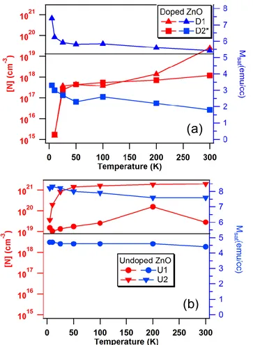
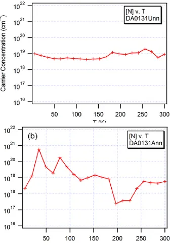
grown by PLD. The samples used were of the same thickness and had carrier concentrations of 2.5x10¹⁸ and 7.3x1019cm-3 for the doped and undoped films.
(4.1.6b). Similar results were obtained for two other doped and undoped ZnO thin films (D2 and U2), the corresponding graphs are shown along with D1 and U1.
Figures for Chapter 4.1
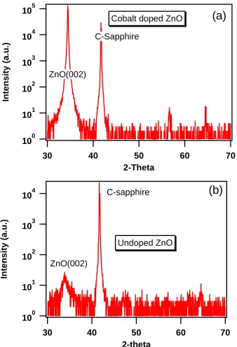
Figure 4.1.1: θ-2θ XRD scans of (a) cobalt doped and (b) undoped ZnO.
100 101 102 103 104 105 In te ns ity (a .u .) 70 60 50 40 30 2-Theta ZnO(002) C-Sapphire
Cobalt doped ZnO
(a)
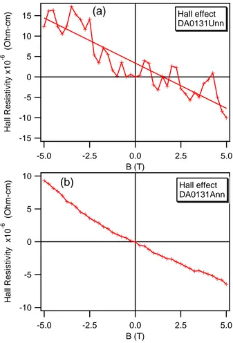
Figure 4.1.3: Hall effect vs. magnetic field of (a) cobalt doped and (b) undoped ZnO.
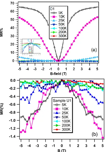
Figure 4.1.5: Temperature dependence of magnetoresistance vs magnetic field for for (a) cobalt doped and (b) undoped ZnO.
-1.4 -1.2 -1.0 -0.8 -0.6 -0.4 -0.2 0.0
M
R(%)
-5 -4 -3 -2 -1 0 1 2 3 4 5
B (T) Sample U1
5K 10K 25K 50K 100K 200K 300K
4.2 PHE in Cobalt Doped ZnO
Figures for Section 4.2
4.3 PHE in Undoped ZnO thin films grown by MOVPE and PLD
Figure 4.3.1 shows the θ-2θ scans of the XRD measurements for ZnO thin films grown on c-plane sapphire by MOVPE and PLD. For the MOVPE grown sample, the θ-2θ scan reveals only (002) and (004) reflections, which is indicative of highly c-axis oriented thin films with good quality. The PLD sample showed a weak intensity (002) peak, which suggests that the sample is nanocrystalline and/or highly textured. Within the detection limits of the XRD system, no secondary magnetic phases are present in the X-ray diffraction patterns.
Figure 4.3.2 shows the variation of resistivity with temperature, which clearly shows characteristic semiconducting behavior expected for ZnO thin films. Although the XRD data of the PLD grown sample suggested a nanocrystalline or highly textured film, this sample exhibited an overall lower resistivity than the MOVPE grown sample over the entire temperature range from 5-300K. In addition, the resistivity of both the samples grown by PLD showed a well-defined exponential behavior which is consistent with simple thermal activation of charge carriers from an unintentional donor level within the band gap to the conduction band.
the magnetic field dependence of the Hall resistivity indicate that both films are n-type semiconductors. In terms of band structure and band filling, stoichiometric ZnO is a wide-band gap semiconductor or might be considered an insulator since the two 4s electrons in Zn are transferred to the oxygen 2p-band, making the valence band completely full. If, however, oxygen vacancies or Zn interstitials are introduced into the crystal lattice through annealing in a reducing atmosphere (causing neutral oxygen to leave the crystal), then the valence electrons of these zinc interstitials can be easily excited and act as donors [17]. In addition, charge neutrality requires that there be a maximum of two electrons along with the oxygen vacancies in the place of the missing oxygen atoms. As a consequence then, in non-stoichiometric ZnO we have a defect structure that has an oxygen vacancy with electrons from the conduction band localized on adjacent zinc sites in the form of Zn+ ions [83]. Therefore, non-stoichiometric ZnO is an n-type semiconductor [17]. Since nominally undoped samples are all n-type, it is likely that they are non-stoichiometric and contain many lattice defects.
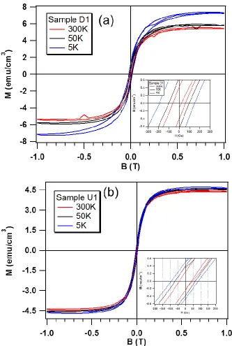
seen in the insets of Fig. 4.3.4. Coercivity is considered the resistance of a ferromagnetic material to becoming demagnetized. There is an expected increase in magnetic ordering as the temperature decreases since thermal fluctuation effects are decreased. This increased ordering may be the reason why coercivity increases at lower temperatures, meaning that the magnetic ordering makes the sample more resistive to demagnetization. Since these samples are both nominally undoped, one must consider other sources for the magnetic behavior since XRD did not reveal the presence of any secondary magnetic phases. It is postulated that the origin of the magnetic behavior in these samples lies in the intrinsic defect structure of these ZnO thin films, specifically oxygen vacancies. Mal, et al previously showed that oxygen vacancies play a key role in the magnetic properties of ZnO [30]. In particular, they demonstrated that one could tune the ferromagnetic behavior in ZnO films by varying the oxygen vacancy content through various annealing steps. Ferromagnetic behavior was enhanced through an increase in oxygen vacancies by thermal annealing and/or laser irradiation [31] or suppressed, that is, it becomes diamagnetic by annealing in oxygen environment [30, 31].
Recently, Choudhury proposed an F-center mediated bound magnetic polaron to explain ferromagnetic behavior in Mn-doped TiO2 nanoparticles [89]. In their model, they suggested that the ferromagnetic ordering is due to the interaction of neighboring Mn2+ ions via an oxygen vacancy (F+ center). Since the samples studied here are magnetically undoped, it is proposed instead that the oxygen vacancy itself is the source of the magnetic moment with the conduction electrons acting as the mediators of the interaction between neighboring oxygen vacancies. This is similar to the carrier-mediated ferromagnetism known as the bound magnetic polaron, in which oxygen vacancies act as both electron donors and electron traps. The trapped electrons couple the local moments in the host lattice within their orbit ferromagnetically leading to a large net magnetic moment [90]. Since the ZnO thin films investigated here exhibited both magnetic and semiconducting properties, it was expected that the planar Hall effect phenomenon would be observed. Measurements were performed to investigate the interaction between magnetization and the current flow direction in our samples. The angular dependence of the PHE is given in Eq. (2) and predicts extrema at angles of 45, 135, 225 and 315o. As shown in Fig. 4.3.5a, these are exactly the angles at which we observe extrema in our nominally undoped films. The acquired data were fitted to a sin2θ curve displayed by the red line in Fig.4.3.5. PHE and AMR can be compared between samples by using the resistivity constant dρ=ρ// - ρ┴ . This constant is the difference between
are in the same order of magnitude with some deviation. Eqs. (1) and (2) are based on the assumption of uniform current; while these films could be inhomogeneous and the role of crystal anisotropy is yet to be studied. Nevertheless it can be see that the values are comparable. The magnetotransport properties of these samples are summarized in table 4.3.1.
Figure 4.3.6 reveals that there is no visible sin2θ behavior at very low fields; this suggests that there is a large randomization of the magnetic moments (very low remnant magnetization) below the saturation field leading to an overall constant resistance even as the direction of current is rotated. An applied field of 1 Tesla, however, is sufficient to produce a saturation magnetization which results in the expected sinusoid of the planar Hall effect. This can be correlated to the M vs. H behavior seen in Fig. 4.3.4, which showed that the magnetization of the MOVPE sample is saturated at ~1000 Oe (0.1 T). It is expected that the PHE angular behavior should be visible at an applied field greater than or equal to this value. In addition to the PHE, AMR data was acquired on these same undoped ZnO films. The angular dependence revealed the expected ~cos2θ behavior as illustrated by the fit of the data in Fig. 4.3.7 to Eq. (1). The AMR plots are complementary to the PHE data since they both originate from the same source, namely the interaction between the magnetization and current applied in the plane of the film as the angle between the two is modulated. Comparing Figs. 4.3.5 and 4.3.7, it was clear that the PHE was the more sensitive of the two anisotropy resistivity phenomena and followed its expected angular dependence much more closely than the AMR data. In terms of sensor applications based on the AMR/PHE, it would be beneficial to measure both simultaneously. Even when the AMR signal is weak and noisy, the PHE is expected to display a strong and clear signal.
present in nominally undoped ZnO. This is intriguing in light of the many reports of the seemingly counterintuitive “d0
Figures for Section 4.3
Figure 4.3.5: PHE vs. angle at 4.2K and 1T, for (a) MOVPE, and (b) PLD ZnO films. -0.20 -0.15 -0.10 -0.05 0.00 0.05 0.10 0.15 RP H E (Ohm s ) 360 315 270 225 180 135 90 45 0
(deg)
MOVPE Sample PHE vs.
(a)
-0.3 -0.2 -0.1 0.0 0.1 0.2 0.3 RP H E (Ohm s ) 360 315 270 225 180 135 90 45 0 (deg)
PLD Sample PHE vs.
Figure 4.3.6: PHE vs. angle at different magnetic field values for MOVPE grown ZnO.
4.4 Effects of Annealing on ZnO Magnetotransport Properties
(Fig. 4.4.6) and AMR (Fig. 4.4.7) signals. The maximum in PHE constant was observed at 5K to be -1.13 Ohms for the unannealed sample and -0.28 Ohms for the annealed. There is a four times larger PHE signal in the unannealed than the annealed sample. This difference is also seen the three times larger AMR signal. At 300K there are large fluctuations in the measurements, these were also seen in other high resistivity samples, this could be caused by the addition thermal agitation at room temperature. The properties of both samples are summarized in table 4.4.1.
Figures for 4.4
Figure 4.4.6: Temperature dependence of PHE vs. angle for (a) unannealed and (b) annealed ZnO thin films.
-0.6 -0.4 -0.2 0.0 0.2 0.4 0.6 RP H E (Ohm s ) 315 270 225 180 135 90 45 0
(deg)
PHE at 7.5T(Unannealed)
5K 10K 25K 50K 100K 200K 300K
(a)
-0.6 -0.4 -0.2 0.0 0.2 0.4 0.6 315 270 225 180 135 90 45 0PHE at 7.5T(Annealed) 5K 10K 25K 50K 100K 200K 300K
Figure 4.4.7: Temperature dependence of AMR vs. angle for (a) unannealed and (b) annealed ZnO. -0.50 -0.25 0.00 0.25 0.50 RA MR (Ohm s ) 270 225 180 135 90 45 0
(deg)
AMR at 7.5T(Unannealed)
5K 10K 25K 50K 100K 200K 300K
(a)
-0.50 -0.25 0.00 0.25 0.50 RA MR (Ohm s ) 270 225 180 135 90 45 0 (deg)
AMR at 7.5T(Annealed) 5K 10K 25K 50K 100K 200K 300K
Table 4.4.1: Summary of magnetotransport properties of unannealed and annealed undoped ZnO thin films
4.5 PHE in SnO2
Following the successful observation of PHE in undoped ZnO, undoped SnO2 was the next metal oxide semiconductor to be studied. SnO2 is one component of the well-known transparent conducting oxide indium tin oxide. The SnO2 samples measured had high carrier concentrations as shown by figure 4.5.1. Resistivity vs. temperature (4.5.2a) and Hall effect measurements (4.5.2b) confirmed that these films were n-type semiconductors. Magnetization vs. magnetic field (4.5.3) showed soft ferromagnetic characteristics with Msat from 5 to 33emu-cm-3 at room temperature. Similar MR behavior to undoped ZnO was also observed (Fig. 4.5.4). The negative MR at 100K and lower was an indication of increasing magnetic ordering. The sinusoids of PHE and AMR were visible starting (Fig. 4.5.5 and 4.5.6) at 100K, and the signals became stronger with decreasing temperatures. At higher temperatures, the angular dependence seemed to be diminished.
Figures for section 4.5
Figure 4.5.1: Carrier concentration vs. temperature for undoped SnO2 thin films
1017
1018
1019
1020
1021
Carrie
r Conc
e
ntra
tio
n
300 250
200 150
100 50
0
Temperature(K) Undoped SnO2
Figure 4.5.2: (a) Resistivity vs. temperature and (b) Hall effect for undoped SnO2 films. 10 9 8 7 6 5 Re s is tiv ity (m cm) 300 250 200 150 100 50 0 Temperature(K)
4.5.4: Temperature dependence of magnetoresistance vs. magnetic field for undoped SnO2 thin films a) R22 and b) R26.
-5 -4 -3 -2 -1 0 M R( % )
5 4 3 2 1 0 -1 -2 -3 -4 -5
B(T) Sample R22 300K 100K 25K 5K
(a)
-6 -5 -4 -3 -2 -1 0 M R(% )-5 -4 -3 -2 -1 0 1 2 3 4 5
4.5.5: Temperature dependence of (a) PHE vs. angle and (b) AMR vs. angle for undoped SnO2 sample R22.
-1.0 -0.5 0.0 0.5 1.0 RP H E (Ohm s ) 315 270 225 180 135 90 45 0
(deg) PHE at 7.5T (R22)
5K 10K 25K 50K 100K 200K 300K
(a)
-0.6 -0.4 -0.2 0.0 0.2 0.4 0.6 RA MR (Ohm s ) 270 225 180 135 90 45 0 (deg) AMR at 7.5T (R22)
5K 10K 25K 50K 100K 200K 300K
4.5.6: Temperature dependence of (a) PHE vs. angle and (b) AMR vs. angle for undoped SnO2 sample R26.
-3 -2 -1 0 1 2 3 RP H E (Ohm s ) 315 270 225 180 135 90 45 0
(deg)
PHE at 7.5T (R26) 5K 10K 25K 50K 100K 200K 300K
(a)
-2 -1 0 1 2 RA MR (Ohm s ) 270 225 180 135 90 45 0 (deg)
AMR at 7.5T (R26) 5K 10K 25K 50K 100K 200K 300K
4.6 PHE in CdO
With the observation of planar Hall effect in undoped ZnO and SnO2, the question arose of whether PHE was intrinsic to conducting oxides. This is what drove the research into cadmium oxide. Interest in CdO came because one of the requirements for observing magnetotransport phenomenon is a satisfactorily conducting oxide. A recent publication by Sachet et al. [95] showed the excellent conducting properties in defect-engineered semiconducting dysprosium doped CdO. The authors showed that doping CdO with a sufficient amount of dysprosium significantly increased the carrier concentration and mobility to the point that it became a degenerate semiconductor with metallic conduction behavior. Because of the defect-engineering of these samples, the question arose of what would be the magnetic properties of Dy:CdO and subsequent magnetotransport phenomena; would it also display planar Hall effect or not?
suppressed by another phenomenon, perhaps the high carrier concentration? Was it possible to actually have AMR in a material without PHE? It seemed reasonable to assume to that AMR could be due to the paramagnetic dysprosium atoms, but it was necessary to break down this question by conducting a series of experiments with samples of different levels of dysprosium doping.
CdO (Fig. 4.6.5b). It seems that the dynamics of magnetotransport in undoped CdO are very different from those in ZnO and SnO2. Another distinguishing feature of CdO is that all the samples have metallic conductivity, whereas ZnO and SnO2 are semiconducting. This may be the main reason why positive MR is prominent in CdO. Since it has such high carrier concentration (>1020 cm-3), higher magnetic fields result in a high degree of electron scattering (positive MR), whereas in ZnO and SnO2, it seems that the higher magnetic field only increases magnetic ordering (negative MR).
this could in turn help to elucidate how electrons or holes contribute to the magnetization
and magnetotransport properties of magnetic conductors. Magnetotransport properties of
CdO are summarized in table 4.6.1.
Figure 4.6.1: Temperature dependence of (a) PHE vs. angle and (b) AMR vs. angle for lowest Dy doped CdO.
-30 -20 -10 0 10 20 30 RP H E (Oh m s ) x 1 0 -3 315 270 225 180 135 90 45 0
(deg) PHE at 7.5T (CdO)
5K 25K 50K 100K 200K 300K
(a)
-6 -4 -2 0 2 4 6 RA MR (Oh m s ) x 1 0 -3 270 225 180 135 90 45 0 (deg) AMR at 7.5T (CdO)
5K 25K 50K 100K 200K 300K
Figure 4.6.2: (a) Resistivity vs. temperature and (b) Hall effect for 300 nm CdO 350 300 250 200 150 100 50 0 Res is ti v ity x 1 0
-6 (Ohm
-c m ) 300 250 200 150 100 50 0 T (K) RvT (300 nm samples)
Undoped Low Dy doped
High Dy doped
-15 -10 -5 0 5 10 15 Hal l Res is tiv ity x 1 0 -6 (O hm -c m ) 5 4 3 2 1 0 -1 -2 -3 -4 -5 B (T)
Figure 4.6.4: (a) MR vs. B-field and (b) resistivity vs. temperature of undoped CdO. Notice resistivity minimum near 120K.
320
300
280
260
240
Res
is
ti
v
ity
x
1
0
-6 (Ohm
-c
m
)
300 250
200 150
100 50
0
T (K) RvT
Undoped
Figure 4.6.5: Temperature dependence of MR vs. B-field for (a) low and (b) high Dy CdO thin films. 5 4 3 2 1 0 -1 M R ( % ) 5.0 2.5 0.0 -2.5 -5.0 B (T) MR (Low Dy CdO)
300K 200K 100K 50K 25K 10K 5K
(a)
8 6 4 2 0 -2 -4 -6 -8 M R (% ) 5.0 2.5 0.0 -2.5 -5.0 B (T) MR (CdO-ES5)300K 200K
100K 50K
25K 10K
5K
Figure 4.6.6: Temperature dependence of (a) PHE vs. angle and (b) AMR vs. angle for undoped CdO. -60 -40 -20 0 20 40 60 RP H E (Ohm s ) x 1 0 -3 315 270 225 180 135 90 45 0
(deg) PHE at 7.5T (Undoped CdO)
5K 10K 25K 50K 100K 200K 300K
(a)
-30 -20 -10 0 10 20 30 RA MR (Ohm s ) x 1 0 -3 270 225 180 135 90 45 0 (deg) AMR at 7.5T (Undoped CdO)
5K 10K 25K 50K 100K 200K 300K
Figure 4.6.7: Temperature dependence of (a) PHE vs. angle and (b) AMR vs. angle for low Dy doped CdO.
12 8 4 0 -4 -8 -12 RP H E (Ohm s ) x 1 0 -3 315 270 225 180 135 90 45 0
(deg) PHE at 7.5T (low Dy CdO)
5K 10K 25K 50K 100K 200K 300K
(a)
-3 -2 -1 0 1 2 3 RA MR (Ohm s ) x 1 0 -3 270 225 180 135 90 45 0 (deg)
AMR at 7.5T (low Dy CdO) 5K 10K
25K 50K 100K 200K 300K
Fig. 4.6.8: Temperature dependence of PHE vs. angle (a) and AMR vs. angle (b) for high Dy doped CdO -6 -4 -2 0 2 4 6 RP H E (Ohm s ) x 1 0 -3 315 270 225 180 135 90 45 0
(deg)
PHE at 7.5T (High Dy CdO)
5K 10K 25K 50K 100K 200K 300K
(a)
-3 -2 -1 0 1 2 3 RA MR (Ohm s ) x 1 0 -3 270 225 180 135 90 45 0 (deg)
AMR at 7.5T (High Dy CdO)
5K 10K 25K 50K 100K 200K 300K
4.7 PHE in CuO
The last material to be studied was copper oxide (CuO) on silicon substrates grown by magnetron sputtering. SEM images showed that these samples were nanocrystalline (Fig. C.1). These samples (50nm thickness) were p-type with very high carrier concentration, 1x1021 cm-3, at room temperature. Hall effect (Fig. 4.7.1a) was used to determine the majority carrier type. This high carrier concentration is usually characteristic of degenerate semiconductors. That is, a semiconductor with such high carrier concentration that it begins to behave like a metal. The resistivity vs. temperature (Fig. 4.7.1b) confirmed this metallic conduction, but with the addition of a resistivity minimum around 100 K and a steady state at 34K and below. There are two common explanations for the appearance of this resistivity minimum: electron-electron interactions and the Kondo effect. The Kondo effect is due to the strong coupling between conduction electrons and magnetic impurities at low temperatures. Kondo explained this behavior as being due to spin-flip scattering between the conduction electrons and the localized spin [97-98]. The theory states that at low temperatures, each local spin becomes locked into a collective state (singlet) with the conduction band spins. At high temperatures, the spin-flip occurs due to thermal energy, but as temperature decreases, the spin-flips become frozen and the Kondo effect saturates. Both the resistivity minimum and saturation are characteristic of the Kondo effects [97, 99].
Figures for Section 4.7
Figure 4.7.1: (a) Hall effect and (b) resistivity vs. temperature for 50 nm CuO -4.5 -3.0 -1.5 0.0 1.5 3.0 4.5 Hal l Re s is ti v ity x 1 0 -7 (O h m -c m )
-1.0 -0.5 0.0 0.5 1.0
B (T) Hall effect Sample 1 Sample 2
(a)
90 80 70 60 50 40 30 Res is ti v ity x 1 0 -6 (O h m -c m ) 300 250 200 150 100 50 T (K) R v TSample 1 Sample 2
Figure 4.7.3: Temperature dependence of (a) PHE vs. angle and (b) AMR vs. angle for sample 1. -1.0 -0.5 0.0 0.5 1.0 RP H E (Ohm s ) 315 270 225 180 135 90 45 0
(deg)
PHE at 7.5T (Sample 1)
5K 10K 25K 50K 100K 200K 300K
(a)
-0.8 -0.6 -0.4 -0.2 0.0 0.2 0.4 0.6 RA MR (Ohm s ) 270 225 180 135 90 45 0 (deg) AMR at 7.5T (Sample 1)
5K 10K 25K 50K 100K 200K 300K
Figure 4.7.4: Temperature dependence of PHE (a) and AMR (b) vs. angle for sample 2. 1.0 0.5 0.0 -0.5 -1.0 RP H E (Ohm s ) 315 270 225 180 135 90 45 0
(deg) PHE at 7.5T (Sample 2)
5K 10K 25K 50K
100K 200K 300K
(a)
-1.2 -0.8 -0.4 0.0 0.4 0.8 RA MR (Ohm s ) 270 225 180 135 90 45 0 (deg) AMR at 7.5T (Sample 2)
5K 10K 25K 50K 100K 200K 300K
CHAPTER 5: CONCLUSIONS
Magnetic semiconductors that display robust ferromagnetism at room temperature or higher can be useful towards the development of spintronic devices, i.e. devices that function by utilizing both charge and spin component of electrons for the transport and storage of information. The major challenge facing the development of such devices include finding materials with Curie temperature greater than or equal to room temperature (300K), and being able to distinguish between their intrinsic magnetic properties and extrinsic(contamination induced) magnetism. Magnetotransport methods are valuable techniques for characterizing thin film materials that are magnetic semiconductors. Since magnetometry only gives results from the bulk of the sample (including sub-layers, i.e. substrates and buffer layers), it becomes increasingly difficult to tell whether the magnetization is due to the thin film only or whether it is due to the sub-layers or unintentional contamination. Magnetotransport techniques are powerful because they provide a method for studying spin-dependent charge transport, whether in-plane or out of the plane of sample of interest.
charge transport. PHE and AMR are techniques in which the magnetic field mainly serves to align the magnetization within the plane of the film. With this arrangement, it is then possible to study the angular dependence (anisotropy) of the magnetization. This phenomenon can be useful in the design of magnetoresistive sensors, especially as read heads for magnetic storage media. In order for these sensors to become useful, the PHE must be demonstrated at room temperature.
PHE and AMR are known by their expected sinusoids. For isotropic materials, PHE is equal to (dρ/2)∙sin2θ, and AMR to ρ┴ + dρ∙cos2θ. This angular dependence can be used to detect the directions of magnetization of magnetic bits or stray magnetic fields within the sensing media. Planar Hall effect was studied and displayed in thin films of defect-engineered magnetic conducting oxides ZnO, SnO2, CdO, and CuO. PHE and AMR were used as complimentary to magnetometry (bulk measurement) to ascertain the existence of charge and spin-dependent transport. Metal oxides, especially transition metal oxides, were chosen as the ideal system for the study of PHE because of the interesting changes in their magnetic and conducting properties due to their defect structures. Thin films of these samples are usually non-stoichiometric and the resulting lattice defects result in charge conducting behavior and different magnetic behaviors. ZnO, SnO2, and CdO have been shown to be n-type semiconductors and exhibit room temperature ferromagnetism when they are in small-dimensions (thin films, nanoparticles, etc.). CuO is an antiferromagnet with differing behavior as temperature decreases.
showed increased ordering at the onset of 100K and below. Although these samples showed ferromagnetic properties at room temperature, it seemed the magnetic ordering was not strong enough to display the PHE sinusoid at T>100K. This lack of strong ordering at higher temperatures is most likely due to the disruption by thermal agitations. When the undoped ZnO was annealed in conditions favoring the incorporation of oxygen, it was shown to have a reduced PHE signal. The incorporation of oxygen brings ZnO closer to stoichiometric ratio, and therefore reduces the amount of defects which are responsible for conduction and magnetism. Although cobalt doped ZnO was shown to have a higher magnetization than the undoped, due to the presence of Co ions, it also had very high resistivity. Its magnetoresistance showed a competition between magnetic ordering and increased carrier scattering. PHE was not observed in Co doped ZnO.
Undoped CdO showed the PHE at 200K to 100K, although its magnetic hysteresis indicated a mixture of paramagnetic and ferromagnetic components. The sign of the PHE constant dρ at 200-100K was positive. At 50K and lower, dρ was negative though. This changing in sign could be linked to the appearance of a resistivity increase below 50K. This was reminiscent of the Kondo effect, which is due to the formation of collective states between magnetic impurities and conduction electrons. Doping CdO with Dy increased its carrier concentration, but it also clouded the PHE signal. There was a certain high amount of Dy that led to a visible PHE signal, but also with reversed PHE constant dρ as in undoped CdO at 200K.
The R vs. T in CuO showed characteristics of Kondo effect with a resistivity minimum at 100K and saturation in resistivity at the lowest temperatures (<34K). It was interesting to note that dρ diminished to a minimum at those low temperatures and became constant. The observation of mixed sign in CdO and only positive in CuO led to the conclusion that the sign of PHE may be a way to tell what role the majority carriers in a material play in the magnetotransport properties at different temperatures. It was discussed that dρ was negative in semiconducting Ga(Mn)As [1] in contrast to ferromagnetic metals, where dρ is usually positive. This may be due to the way that electrons and holes contribute differently to spin-orbit coupling in ferromagnetic materials. Future studies could look at how the sign of dρ varies between different materials; this could in turn help to elucidate how electrons or holes contribute to the magnetization and magnetotransport properties of magnetic conductors.
CHAPTER 6: FUTURE WORKS
In order to further the PHE studies in ZnO, it would be advised for future works to look at different post-growth annealing conditions that could enhance the ferromagnetic and conducting properties of this material. Oxygen annealing was shown to reduce the PHE signal, and it is expected that vacuum annealing or laser annealing would enhance this signal. The same studies can be pursued for SnO2, since its results were similar to that of ZnO.
For undoped CdO, more can be done towards studying its PHE when it is grown in different conditions. No work was done specifically towards exploring the effects of high or low carrier concentrations in undoped metal oxides, but CdO could be the ideal material for these studies. Additionally it would be interesting to study the effects of thickness on the strength of the PHE signal.
Undoped CuO was the only material to show PHE at room temperature and is therefore the most interesting and the most promising for future device related studies. Since CuO is antiferromagnetic it would be useful to study whether its presence along with p-type conductivity in other samples could similarly lead to room temperature PHE.
REFERENCES
1. H. X. Tang, R. K. Kawakami, D. D. Awschalom, and M. L. Roukes, Giant Planar Hall Effect in Epitaxial (Ga,Mn)As Devices, Phys. Rev. Lett. 90, 107201 (2003).
2. S. Cass and B. Christie, IEEE Spectrum 40 (7), P.18 (2003) .
3. Q. Xu, H. Schmidt, S. Zhou, K. Potzger, M. Helm, H. Hochmuth, M. Lorenz, A. Setzer, P. Esquinazi, C. Meinecke, M.Grundmann, Appl. Phys. Lett. 92, 082508 (2008).
4. A. Gupta, Novel room-temperature ferromagnetic semiconductors, Doctoral Dissertation, Royal Institute of Technology, Stockholm, Sweden, June 2004.
5. F. Matsukura, H. Ohno, and T. Dietl: “III-V Ferromagnetic Semiconductors” in
“Handbook of Magnetic Materials” vol. 14, ed. By K.H.J Buschow (Elsevier, Amsterdam 2002) P. 1-87.
6. K. Ando, Science 312, 1883 (2006).
7. A. Bonanni and T. Dietl, Chem. Soc. Rev. 39, 528 (2010).
8. Z. Zuo, M. Morshed, W.P. Beyermann, J.-G. Zheng, Y. Xin, J. Liu, AIP Adv. 3, 032110 (2013).
9. T. Dietl, H. Ohno, F. Matsukura, J. Cibert, and D. Ferrand, Science 287, 1019 (2000). 10. Y. Bason, L. Klein, J.-B. Yau, X. Hong, and C. H. Ahn, Appl. Phys. Lett. 84, 2593 (2004).
11. P. Cieranu: “Magnetoresistive Sensors” in “Thin Film Resistive Sensors,” ed. by and P. Cieranu and S. Middlehoek(Institute of Physics Publishing, Bristol, 1992) P. 258-262. 12. T.R. McGuire and R. I. Potter, IEEE Trans. Magn. 11, 1018 (1975).
14. A.O. Adeyeye, M.T. Win, T.A. Tan, G.S. Chong, V. Ng, T.S. Low., Sensors Actuat A-Phys. 116, 95 (2004).
15. A. Roy, and P.S.A. Kumar, J. Phys. D: Appl. Phys. 43, 365001 (2010).
16. A. Schuhl, F.N.Van Dau, and J.R. Childress, Appl. Phys. Lett. 66, 2751 (1995). 17. R.E. Hummel, Electronic Properties of Materials, 3rd Edition (Springer, New York, 2005), p. 178, 413.
18. S. J. Pearton, D. P. Norton, K. Ip, Y. W. Heo, and T. Steiner, J. Vac. Sci. Technol. B 22, 932 (2004).
19. C. Liu, F. Yun and H. Morkoç, J. Mater. Sci. Mater. Electron. 16, 555 (2005). 20. Q. Xu, L. Hartmann, H. Schmidt, H. Hochmuth, M. Lorenz, R. Schmidt-Grund, C. Sturm, D. Spemann, M. Grundmann and Y. Liu, J. Appl. Phys. 101, 063918 (2007).
21. D. P. Norton, M. Ivill, Y. Li, Y. W. Kwon, J. M. Erie, H. S. Kim, K. Ip, S. J. Pearton, Y. W. Heo, S. Kim, B. S. Kang, F. Ren, A. F. Hebard, and J. Kelly, Thin Solid Films 496, 160 (2006).
22. J.G. Reynolds, C.L. Reynolds Jr., A. Mohanta, J.F. Muth, J.E. Rowe, H.O. Everitt, D.E. Aspnes, Appl. Phys. Lett. 102, 152114 (2013).
23. Z. Zuo, H. Zhou, M. J. Olmedo, J. Kong, W. P. Beyermann, J. G. Zheng, Y. Xin, and J. Liu, J. Appl. Phys. 112, 053708 (2012).
24. Z. Yang, J. L. Liu, M. Biasini, and W. P. Beyermann, Appl. Phys. Lett. 92, 042111 (2008).
26. Z. Yang, W. P. Beyermann, M. B. Katz, O. K. Ezekoye, Z. Zuo, Y. Pu, J. Shi, X. Q. Pan, and J. L. Liu, J. Appl. Phys. 105, 053708 (2009).
27. J. H. Kim, H. Kim, D. Kim, Y. E. Ihm, and W. K. Choo, Physica B 327, 304 (2003). 28. P. Pant, J. D. Budai, and J. Narayan, Acta Mater. 58, 1097 (2010).
29. W. Wei, S. Nori, C. Jin, J. Narayan, R. J. Narayan, D. Ponarin, and A. I. Smirnov, Mater. Sci. Eng., B 171, 90 (2010).
30. S. Mal, S. Nori, C. Jin, J. Narayan, S. Nellutla, A. I. Smirnov, and J. T. Prater, J. Appl. Phys. 108, 073510 (2010).
31. S. Mal, J. Narayan, S. Nori, J.T. Prater, and D. Kumar, Solid State Commun. 150, 1660 (2010).
32. C. Jin, R. Narayan, A. Tiwari, H. Zhou, A. Kvit, and J. Narayan, Mater. Sci. Eng. B 117, 348 (2005).
33. K. T. Roro, G. H. Kassier, J. K. Dangbegnon, S. Sivaraya, J. E. Westraadt, J. H. Neethling, A. W. R. Leitch, and J. R. Botha, Semicond. Sci. Technol. 23, 055021 (2008). 34. R. Cebulla, R. Wendt, and K. Ellmer, J. Appl. Phys. 83, 1087 (1998).
35. J. M. D. Coey, Curr. Opin. Solid State Mater. Sci. 10, 83 (2006).
36. J. H. Krieger and S. M. Spitzer, "Non-traditional, Non-volatile Memory Based on Switching and Retention Phenomena in Polymeric Thin Films", Proceedings of the 2004 Non-Volatile Memory Technology Symposium, IEEE, pp. 121, 2004.
37. Y. Huai, AAPPS Bull. 18, 33 (2008).
38. Y. V. Pershin and M. Di Ventra, Phys. Rev. B 77, 073301 (2008).