ABSTRACT
PEARCE, BRADY LAWRENCE. Solution Based Functionalization of Nanostructured Oxides with Organic Molecules. (Under the direction of Dr. Albena Ivanisevic).
The surface modification of wide bandgap semiconductors with organic molecules provides novel functionalities to the composite material. These functionalities can include tuning of the optical properties, providing solution stability of the inorganic material, as well as many others. The use of an in-situ functionalization method for surface attachment of phosphonic group containing molecules to the surface of gallium nitride (GaN) has shown promise. This technique is particularly advantageous due to the etching and functionalization steps occurring at the same time, in the same beaker, as well as not being reliant on organic solvents or high temperatures. In this functionalization process, surface hydroxide groups are preferentially grown on the surface of GaN, which serve as attachment sites for phosphonic groups on organic moieties. Molecules with these hydroxyl groups available natively on their surface, such as AlOOH and GaOOH, provide a unique advantage. The requirement for an etching step is removed, and the functionalization process could be performed in a simple one-step modification. The work in this dissertation seeks to address the possibility of using these materials as the inorganic component in organic/inorganic composite material in devices. Of particular importance in solar cell and bioelectronic devices is the ability to withstand varying pH environments, and to avoid the leaching of toxic ionic species. Lysine has shown to reduce the leaching of ionic species, when particles of inorganic molecules are cross-linking agents for the amino acid. In this work, the aqueous stability of both AlOOH and GaOOH in a lysine environment will be explored. The optical and size characteristics observed in nanostructured forms of the mixed composition AlxGa1-xOOH material system is
containing these organic/inorganic hybrids. Immobilizing phosphonic group containing organic dyes on the surface of GaN, GaOOH, AlOOH and mixed compositions of AlGaOOH using surface bonding sites, and possible covalent attachments mechanisms, seeks to provide an improvement in the long term stability of the inorganic/organic interface for devices. Future work in this area will test device efficiency using these hybrids, explore additional mixed oxyhydroxide composition systems and continue the advancement of the
understanding of the important role of phosphonic groups in organic/inorganic devices. The nature of chemical and surface species in these materials will be characterized with Fourier Transformed-Infrared Spectroscopy (FT-IR) and X-Ray Photoelectric Spectroscopy (XPS). The optical properties of the materials were tested with photoluminescence (PL)
spectroscopy, and the stability was examined with fluorescence spectroscopy. The crystallographic nature of the nanostructured inorganic materials before and after functionalization was determined with X-Ray Diffraction (XRD). Images of the
Solution Based Functionalization of Nanostructured Oxides with Organic Molecules
by
Brady Lawrence Pearce
A dissertation submitted to the Graduate Faculty of North Carolina State University
in partial fulfillment of the requirements for the degree of
Doctor of Philosophy
Materials Science and Engineering
Raleigh, North Carolina 2016
APPROVED BY:
_______________________________ _______________________________
Dr. Albena Ivanisevic Dr. Michael Dickey
Committee Chair
_______________________________ _______________________________
ii BIOGRAPHY
Brady Pearce was born in Waukesha, Wisconsin and moved to the Raleigh, North Carolina area when he was 8 years old. He did his undergraduate at Appalachian State University as a
double major in physics and chemistry. Brady also received a master’s degree from
Appalachian State in engineering physics. He worked with Albena Ivanisevic on surface functionalization of synthesized nanostructured oxyhydroxide materials at North Carolina
iii TABLE OF CONTENTS
LIST OF TABLES ... vi
LIST OF FIGURES ... vii
1. Introduction ... 1
1.1 Background ... 1
1.2 Gallium Nitride, Gallium Oxyhydroxide and Aluminum Oxyhydroxide... 2
1.3 In-situ Functionalization of Gallium Nitride Using the Surface Oxide Layer ... 3
1.4 Applications of Organic/Inorganic Composites ... 5
1.5 Advantages of Nanostructured Materials ... 7
1.6 Examples of Synthesis Techniques for Nanostructured Materials ... 7
1.6.1 Solution Based Techniques ... 7
1.6.2 Microwave Hydrothermal Synthesis... 9
1.7 Advantages of Oxide Materials for Functionalization ... 10
1.8 Characterization Methodologies and Properties of Organic/Inorganic Interfaces .... 11
1.8.1 X-Ray Photoelectron Spectroscopy ... 11
1.8.2 X-Ray Diffraction ... 13
1.8.3 Optical Properties and Photoluminescence Spectroscopy ... 13
1.8.4 Stability and Fluorescence Spectroscopy ... 14
1.8.5 Scanning Electron Microscopy ... 15
1.9 Summary and Overview ... 15
2. In-situ Functionalization of Gallium Nitride Powder with a Porphyrin Dye ... 17
2.1 Abstract ... 17
2.2 Introduction ... 17
2.3 Materials and Methods ... 20
2.3.1 Powder Functionalization ... 20
2.3.2 Characterization ... 20
2.4 Results and Discussion ... 22
2.4.1 In-Situ Functionalization of GaN Powder with Porphyrin ... 22
2.4.2 Stability of Porphyrin in Phosphoric Acid ... 24
2.4.3 Morphological Characterization by SEM ... 25
iv
2.5.1 X-Ray Photoelectron Spectroscopy ... 26
2.5.2 Infrared Spectroscopy ... 32
2.5.3 Stability Testing Using Fluorescence Spectroscopy ... 34
2.6 Conclusion ... 36
3. In-situ and Ex-situ Functionalization of Nanostructured Gallium Oxyhydroxide with a Porphyrin Dye ... 37
3.1 Abstract ... 37
3.2 Introduction ... 38
3.3 Materials and Methods ... 40
3.3.1 Microwave Synthesis and Functionalization ... 40
3.3.2 Characterization ... 41
3.4. Results and Discussion ... 43
3.4.1 Synthesis and Functionalization with Porphyrin Dye ... 43
3.4.2 Crystallographic Characterization with XRD ... 47
3.4.3 Optical Properties... 51
3.4.4 Surface Characterization by X-Ray Photoelectron Spectroscopy ... 54
3.4.5 Fourier Transformed-Infrared Spectroscopy ... 61
3.4.6 Stability Testing Using Fluorescence Spectroscopy ... 63
3.5 Conclusions ... 64
4. Synthesis and Optical Characterization of Mixed Nanostructured Aluminum-Gallium Oxyhydroxide ... 66
4.1 Abstract ... 66
4.2 Introduction ... 66
4.3 Results ... 68
4.4 Conclusions ... 74
5. Aqueous Stability of Nanostructured Aluminum and Gallium Oxyhydroxide Before and After Functionalization with Lysine ... 76
5.1 Abstract ... 76
5.2 Introduction ... 77
5.3 Materials and Methods ... 79
5.3.1 Synthesis of AlOOH and GaOOH Nanostructured Materials and Lysine Composites ... 79
v
5.4 Results and Discussion ... 80
5.4.1 X-Ray Diffraction ... 81
5.4.2 X-Ray Photoelectron Spectroscopy ... 82
5.4.3 Fourier-Transformed Infrared Spectroscopy ... 84
5.4.4 Inductively Coupled Plasma-Mass Spectrometry Aqueous Stability ... 85
5.5 Conclusions ... 86
6. Optical Property Modulation from In-situ and Ex-situ Functionalization of Nanostructured Mixed Oxyhydroxides with a Porphyrin Dye... 88
6.1 Abstract ... 88
6.2 Introduction ... 90
6.3 Materials and Methods ... 91
6.3.1 Synthesis of Organic/Inorganic Composites ... 91
6.3.2 Characterization ... 91
6.4 Results and Discussion ... 92
6.4.1 X-Ray Diffraction ... 92
6.4.2 Fourier-Transformed Infrared Spectroscopy ... 93
6.4.3 Size Measurements from Scanning Electron Microscopy ... 94
6.4.4 Optical Properties of Composites Using Photoluminescence ... 95
6.5 Conclusions ... 98
7. Conclusions and Future Outlook ... 99
vi LIST OF TABLES
Table 3.1. FWHM of the peaks used and the qualitative crystallite sizes calculated from them... 50 Table 3.2. Atomic percentages of C, O, N, Ga, Na and P of the precursor Ga(NO3)3, the
TTP-PO3 salt, clean GaOOH and in-situ and ex-situ GaOOH/TTP-PO3. ... 56
Table 3.3. Atomic ratios of O to Ga, C to Ga and N to Ga for the precursor Ga(NO3)3, clean
GaOOH and in-situ and ex-situ GaOOH/TTP-PO3 ... 57
Table 3.4. The contribution of environment N, Ga LMM auger, pyrolle and satellite N peaks in percentages of N 1s spectra of clean GaOOH, in-situ and ex-situ GaOOH/TTP-PO3. ... 60
Table 3.5. The contribution of the Ga-O, OH and P-O peaks in percentages of the O 1s spectra for the clean GaOOH and the in-situ and ex-situ GaOOH/TTP-PO3. ... 61
Table 4.1. Displayed are the DLS measurements of the average diameter of the mixed oxides. ... 69 Table 4.2. ICP-MS data of Al and Ga leaching of the mixed oxides. ... 74 Table 5.1. Displayed is the ICP-MS data for Day 1, 5 and 7 of the various solutions of the submerged materials and the measured Ga or Al concentrations and percent of starting
vii LIST OF FIGURES
Figure 2.1. Schematic diagram of the in situ functionalization process showing bidentate binding of the porphyrin on the surface of the GaN powder. ... 24 Figure 2.2. Room temperature UV-Vis spectra of (a) 7.125 μM TTP-PO3 in DI water and (b)
50% 7.125 μM TTP-PO3 in DI water and 50% phosphoric acid. ... 25
Figure 2.3. SEM image of GaN powder showing the size and heterogeneity of aggregrates within the powder. Scale bar is 5 μm. ... 26
Figure 2.4. Ga 2p regional XPS spectra of (a) clean GaN powder, (b) clean, etched GaN powder, and (c) functionalized GaN powder. ... 28 Figure 2.5. C 1s regional XPS spectra of (a) clean GaN powder, (b) clean, etched GaN powder, and (c) functionalized GaN powder. ... 29 Figure 2.6. P 2p regional XPS spectra of (a) clean GaN powder, (b) clean, etch GaN powder, and (c) functionalized GaN powder. ... 30 Figure 2.7. N 1s regional XPS spectra of (a) clean GaN powder, (b) clean etched GaN
powder, and (c) functionalized GaN powder. Peak assignments are displayed with the peak near 400.8 eV present only in the functionalized powder. ... 31 Figure 2.8. FTIR regional scan between 3000 and 1200 cm-1 of KBr mixed with (a)
functionalized powder and (b) TTP-PO3. ... 34
Figure 2.9. Fluorescence spectroscopy spectra of (a) 7.125 μM solution of TTP-PO3 in DI
water, (b) sonicated solution of functionalized powder in DI water, and (c) wash of
functionalized powder in DI water after 20 days. ... 36 Figure 3.1. SEM images of (a) clean GaOOH nanorods, (b) ex-situ GaOOH/TTP-PO3 and (c)
in-situ GaOOH-TTP/PO3. ... 45
Figure 3.2. Scheme depicting the covalent interaction between TTP-PO3 and the GaOOH
nanorods pictured in the SEM image. ... 46 Figure 3.3. Optical photograph of the clean GaOOH, in-situ and ex-situ GaOOH/TTP-PO3
submerged in DI water in quartz cuvettes... 47 Figure 3.4. XRD spectra of the various GaOOH containing samples along with the Ga(NO3)3
viii Figure 3.5. PL spectra of the dilute TTP-PO3 solution, clean GaOOH, and the ex situ and in
situ GaOOH/TTP-PO3. ... 52
Figure 3.6. XPS spectra of the (a) N 1s of the precursor Ga(NO3)3, clean GaOOH, and the in
situ and ex situ GaOOH/TTP-PO3, (b) O 1s and (c) C 1s of the precursor Ga(NO3)3, TTP-PO3
salt, clean GaOOH, and the in situ and ex situ GaOOH/TTP-PO3 and (d) Ga 2p of the
precursor Ga(NO3)3, clean GaOOH and the in situ and ex situ GaOOH/TTP-PO3. ... 59
Figure 3.7. FT-IR spectra of the in-situ and ex-situ GaOOH/TTP-PO3 as well as the clean
GaOOH sample. ... 62 Figure 3.8. Fluorescence spectroscopy data of the dilute TTP-PO3 solution along with the
shaken in-situ and ex-situ GaOOH/TTP-PO3 in DI water and the wash of the in-situ and
ex-situ GaOOH/TTP-PO3. ... 64
1 1. Introduction
1.1 Background
The main topic of this thesis involves a discussion of the viability of nanostructured gallium and aluminum oxyhydroxide materials, functionalized with organic molecules, as organic/inorganic interfaces for solar cell and biological applications. The use of dyes as the organic molecule in these interfaces presents one particular example, for use as
dye-sensitized solar cells (DSSCs). Dyes with functional groups containing phosphonic sites provide the advantage of binding with the oxide layer native on GaOOH and present through controlled etching on GaN. Previous work has demonstrated the viability of using
phosphonic group containing organics for the functionalization of GaN.1 This covalent bond presents the unique advantage of prolonged device stability in environmental and biological conditions, such as those solar cells and biosensors are subject to.
2 GaOOH, as well as the native layer on AlOOH, presents a unique advantage of these
materials for modification with functional organics.
1.2 Gallium Nitride, Gallium Oxyhydroxide and Aluminum Oxyhydroxide
Gallium nitride belongs to the class of materials known as III-nitrides, containing Ga as the III-group element. The crystal structures that GaN predominately exists in are wurtzite and zinc blende. 3 It is a direct, intrinsic semiconductor with a wide band gap of 3.4 eV.4 As a direct bandgap containing semiconductor, it is suitable as a material for optoelectronic
applications. The incorporation of functional groups to the surface of GaN has been used for a multitude of applications including thin films deposited on nanowires by atomic layer deposition,5 field-effect transistors with recognition peptides attached to the surface,6 thiol groups,7 attachment of olefins,8 alkyl groups,9 incorporation of alkylphosphonic acids10 and 1-alkenes11 in an effort to add various functionality to the inorganic semiconductor surfaces.
The wide bandgap semiconductor, GaOOH, with a bandgap of 4.75 eV, provides a useful inorganic scaffold for the attachment of organic dyes for use as DSSCs and biosensing applications. The crystallinity of GaOOH has been shown to be that of an orthorhombic crystal system.12 In recent work, GaOOH has been used as a precursor molecule for conversion to gallium oxide (Ga2O3)13 as well as GaN.14 With a direct bandgap, GaOOH is
3 materials have been identified as some of the most important compounds for driving the future of optoelectronic devices.16
It is of interest to investigate composite oxyhydroxide materials containing both Ga and Al. The aluminum oxide layer has shown to be an effective and highly stable material for interfacing with organics, such as poly-L-lysine.17 Vogelson et. al. demonstrated the use of a simple reflux reaction to synthesize hybrids of AlOOH and lysine. This technique is
environmentally friendly due to it relying on only DI water as a solvent. The temperatures used are lower than typical functionalization reactions, as well. By replacing the AlOOH nanoparticles with GaOOH nanostructured materials, it is believed that a composite with Ga can be synthesized.
1.3 In-situ Functionalization of Gallium Nitride Using the Surface Oxide Layer Wide bandgap semiconductors are effective materials for functionalization with organic molecules for a number of reasons. The material properties of the inorganic
semiconductor form the basis for optical and electrical characteristics of the functional device as well as determine the coherency of the interface between the two molecules. In the case of GaN and GaOOH, the effectiveness and stability of the interface is reliant on the oxide layer present on the surface of the two molecules. Hydroxide groups present on the surface have proven effective moieties for the attachment of phosphonic groups and covalent modification of the surface with an organic molecule.18
4 characterized to determine differences before and after the modification. Changes in the optical properties due to the functionalization have been explored in detail due to the materials importance in light emitting diodes (LEDs).19
The mechanism of the in-situ surface attachment of organic moieties to GaN consists of a few steps for coverage to occur. It is noted that this approach is less time consuming and more environmentally friendly than previous reported methods of functionalization of
semiconductors with organic molecules. There are four steps in this process including cleaning, etching and binding of the functional molecule and capping of the surface. During the cleaning process, any environmentally formed, uncontrolled oxide and carbon layer is removed from the surface to ensure a useful oxide layer can be formed for surface
attachment. In the etching portion, oxides are formed and dissolved on the surface of the GaN sample and a controlled attachment layer is formed on the surface. In the in-situ
functionalization of GaN, this etching step is done in conjunction with the binding step where the functional groups used for attachment interact and bind with the controlled oxide layer or, in some cases, the metal itself. Capping is done to ensure that no undesired molecules bind with the surface after the functionalization and any unreacted materials are washed and filtered away.
5 1.4 Applications of Organic/Inorganic Composites
One of the specific applications of interest for these novel, nanostructured organic/inorganic interfaces is that of DSSCs. Since these devices advent in 1991, in the work done by Grätzel and O’Regan20, extensive research has been done to improve the efficiency and stability of them. For DSSCs, the focus of most recent research efforts is on the materials TiO221and ZnO.22 Research into alternative materials has garnered recent
attention due to TiO2 having relatively low electron mobility.23 Conversion efficiencies of the
alternative ZnO have been cited as being low with the reasoning behind this being the dye interaction with the semiconductor at the surface.24 Group III-nitride semiconductors, particularly in nanostructured form, have been identified as extremely important for devices which rely on optoelectronic phenomenon.16 As indicated earlier, the oxide layer present on GaN provides the ability to bond phosphonic containing groups to the surface, thus
increasing efficiency by increasing long term device stability.2
6 proximity of the dye. An electrolyte solution is used to regenerate electrons in the system by reducing them to the lowest occupied molecular orbital (LUMO) of the dye molecule. It is the incoming radiation that promotes these electrons from the LUMO to the HOMO where the dye-semiconductor transfer will occur again. The electrodes of DSSC are typically made of a transparent conducting oxide (TCO).
The typical method of attachment of dye molecule to semiconductor is by
physisorption on the surface by various techniques. This has proven to be a useful technique; however issues of long term stability remain problematic. Recent work has been done to replace the solvent used in the electrolyte solution to address this.28 We seek to add to this by using our unique interface which contains surface bonding and is believed to be capable of long term device stability in environmental conditions.
A second consideration for device implementation is the electronic and optical properties of direct wide bandgap semiconductors providing a method of incorporating an optically active organic molecule to tune these properties for sensing and energy harvesting. The band alignment that occurs between organic dye molecules and GaN and GaOOH is advantageous when compared to that of TiO2. The band alignment of these wide band gap
semiconductors provides evidence of these Ga containing semiconductors viability as suitable replacements for DSSCs.
Beyond solar cells, these organic/inorganic hybrid materials have been identified as especially useful for biosensors and other biological applications. The use of gallium containing materials for biological applications is viable due to its reported
7 applications of these composites. It has shown to improve cell adhesion30 and
biocompatibility31 of various functional materials.
The aqueous stability of materials used in biological applications is important for toxicity considerations. Pourbaix diagrams of Al and Ga oxide materials demonstrate the importance of stabilizing these materials in aqueous environments. Both elements are passivated in small pH windows and in environments with varying pH, leaching of both is likely to occur. This is indicative of improving the stability of oxides of these materials by functionalization with a molecule such as lysine.
1.5 Advantages of Nanostructured Materials
A distinct advantage of the use of nanostructured materials for organic
functionalization is the increased surface area and, therefore increased attachment sites for modification.21 Specifically for photovoltaic applications, there is an increase in research for the use of GaN nanostructured materials. Various nanostructures of GaN have been
investigated including nanobelts, nanowires and others. A microwave hydrothermal process has been used to synthesize nanorods of GaOOH.31 Nanostructured AlOOH has been synthesized using a variety of methods, including the hydrothermal synthesis of γ-AlOOH nanotubes and nanorods.32
1.6 Examples of Synthesis Techniques for Nanostructured Materials 1.6.1 Solution Based Techniques
The literature describing various solution based techniques of forming nanostructured materials is extensive. Examples of solution based methods include microemulsion,
8 microwave hydrothermal synthesis which will be the focus of the next section. Hydrothermal synthesis techniques for metal oxide materials have recently been reviewed.34 Typically, these reactions use metal nitrate salts as precursors. A hydrolysis reaction follows which forms a metal hydroxide. Dehydration of this hydroxide forms a precipitate which is that of a metal oxide. This is described below in Equation 1 and 2, adapted from Hayashi et. al.34
M(NO3)x + xH2O → M(OH)x + xHNO3 (1)
M(OH)x → MOx/2 + x/2 H2O (2)
Microemulsion techniques rely on three different components within one stable, single phase solution. A surfactant is used that is miscible in the solution along with two other components which are not. The stabilizer or emulsifier is a molecule with a polar head group and nonpolar tail. The emulsifier aligns itself with the nonpolar tail facing towards the surfactant and the polar head group facing towards what is typically an aqueous solution containing precursor materials. The emulsifier surrounds the reaction solution and dictates the size and shapes of crystallized product.
Sol-gel techniques rely on the polymerization of inorganic materials. The precursor materials in these reactions form gels through a hydrolysis reaction. The size of the particles is affected by rates of the hydrolysis reaction as well any condensation reactions that occur.33 The removal of solvent from the gel is done using high temperature calcination. Other factors that affect the size of these particles are the composition and pH of the solution and the temperature of the reaction.33
9 with no added pressure or temperature to the reaction. The high energy sound waves cause acoustic cavitation to occur which forms bubbles in the solution which continue to grow until they collapse.33 These bubbles are thought to produce extremely high temperatures during the process of their collapse which are then rapidly cooled back to the ambient solution
temperature.
1.6.2 Microwave Hydrothermal Synthesis
In traditional hydrothermal synthesis techniques, the solution is sealed and placed into an autoclave. The reaction temperature is set and it is left for periods of around 24 hours, typically. Recent work has shown that by replacing the autoclave with a microwave, these reactions can be done in less than an hour.31 This can be done with no surfactant in an environmentally friendly way, with just DI water as a solvent.
The key advantage of microwave synthesis is the drastically reduced time restraints on the reaction process. Along with this, the process requires less energy than typical
synthetic techniques which allows it to be considered a green chemistry technique.35 Another advantage is that the microwave heating is capable of restricting the side reactions that take place during the synthesis.36
Radiation that resides in the frequency range between 0.3 and 300 GHz is considered microwave radiation. The two processes involved in microwave heating are dipolar
10 short periods of time, an advantage of microwave heating that cannot be reproduced by any other method. The various mechanisms behind the microwave’s ability to drastically reduce
reaction time are still under investigation with various theories explaining this phenomenon. 1.7 Advantages of Oxide Materials for Functionalization
The majority of previous research in solution based in-situ functionalization has focused on using GaN as the inorganic moiety of the hybrid material. The surface oxide layer that forms during the etching process has been hypothesized to be GaOOH or various other hydroxyl groups due to the high solubility of Ga2O3 in acidic conditions. It is beneficial,
therefore, to investigate the solution based functionalization of GaOOH (as well as AlOOH) due to the inherent presence of this oxide layer with no etchant required. These materials could be functionalized with soluble phosphonic group containing molecules by simple prolonged contact in solution. This would eliminate any need for harmful etchants or cleaning agents and require simply DI water as a solvent. This process represents a highly scalable and environmentally friendly technique for forming organic/inorganic hybrids with long term interface stability.
11 microwave precursors and the resulting product will be the desired inorganic/organic
composite material.
1.8 Characterization Methodologies and Properties of Organic/Inorganic Interfaces Various techniques exist which have proven effective at investigating the properties of organic/inorganic hybrid materials. Surface sensitive techniques for determining the chemical properties of the interfaces provide important information. This can be done using X-ray photoelectron spectroscopy (XPS) and Fourier transformed-infrared spectroscopy (FT-IR). The effects of functionalization on the crystalline nature of the inorganic materials are of particular interest for the synthesized nanostructures. X-ray Diffraction (XRD) measurements provide this information. The optical properties of the material are the main focus of their viability in optoelectronic devices. The emission wavelength under high energy photon excitation is of particular interest and can be measured using photoluminescence spectroscopy (PL). The stability of the organic material’s attachment to the inorganic
material can be assessed with experiments involving the use of fluorescence spectroscopy. High resolution atomic leaching and ratios can be obtained using inductively coupled plasma-mass spectrometry (ICP-MS). The morphological features of these nanostructured samples can be explored using scanning electron microscopy (SEM).
1.8.1 X-Ray Photoelectron Spectroscopy
12 removed electron will have a kinetic energy which is equal to the energy of the incoming photon minus the binding energy of the electron within the material.38 This energy is
measured and provides information about the atom and orbital shell attributed to the ejected electron. Observed energy shifts in these measured electrons are attributed to binding with various other atomic species.
Two x-ray sources are typically used in XPS instrumentation which includes Al Kα
and Mg Kα. The energy of x-rays generated from these sources is 1486.7 and 1253.6 eV, respectively. Survey scans sweep through a large range of binding energies. These scans can be used for qualitatively understanding the atomic species present on the surface as well as quantitatively measuring the ratio of these species in the sample. Charging effects from insulating samples (such as GaN and the oxide materials of interest) cause the measured binding energies to shift from their real values. Due to this, a calibration standard has been established using the advantageous carbon peak in the carbon 1s regional scan to 284.8 eV.39
13 1.8.2 X-Ray Diffraction
Crystallographic information is of importance for these composites in order to observe the effects, if any, of the presence and attachment of the organic molecule to the crystalline nature of the nanostructured inorganic semiconductors. XRD is a widely used technique for addressing the crystalline nature of samples. In this work, Bragg-Brentano geometry will be the focus of discussion, since the materials are powders and nanostructured samples and not thin films. In this geometry, the angle of diffraction of the x-ray after interacting with the crystal structure of the material provides information about the
orientation and planar spacing of the sample. In addition, the size of crystallites within the material can be determined using the Scherrer equation. The broadening of the spectral lines in the XRD can be used to calculate the size of crystallites.
1.8.3 Optical Properties and Photoluminescence Spectroscopy
A main focus of this chapter is the ability to use the inorganic/organic hybrids
discussed in this work as optoelectronic and biosensing platforms for improving stability and, possibly, efficiency of devices. Of particular interest for these devices is the band matching between the semiconductor and optically active organic molecule. The interaction between the HOMO level of the organic material and the conduction band of the semiconductor provides the basis for electron transfer between the two molecules in devices such as DSSCs. One method of exploring the direct band gap of a semiconductor is by measuring the
emission wavelength seen in a PL spectrum.
14 photon is higher than the band gap of the semiconductor, the material will absorb it and release the energy in a number of different ways. Nonradiative recombination of the excitons releases phonons which is essentially the release of heat through lattice vibrations. In the case of radiative recombination, photons are release from the material and can be measured using a photodetector.
The maximum energy of the photons released from the material are from an exciton pair recombining across the full bandgap of the material. These are referred to as band edge recombinations and are seen at the lowest wavelength in PL spectra. For materials which are made with less regard to defect density as pristine wafers, the PL spectrum is broad and spans a wide range of wavelengths. The second, broad peak seen in these spectra is attributed to exciton recombination within defects levels which lie within the band gap themselves. Therefore, the photons emitted from these recombination processes have lower energy levels than the band edge and are seen at higher wavelengths.
An important consideration of PL measurements is size effects of nanoscale
semiconducting materials. The dominant effect of size characteristics on the band gap of the materials is determined by the size ratio to the Bohr radius of the material as well as the general shape the materials conform to.
1.8.4 Stability and Fluorescence Spectroscopy
15 the presence of soluble organic dye leached off of the semiconductor into solution. This can be accomplished by leaving the composite sedimented in solution for a long period of time. After filtering this solution to ensure none of the sediment remains, fluorescence
spectroscopy can be done to determine if any soluble dye has leached off of the semiconductor and into solution.
1.8.5 Scanning Electron Microscopy
Imaging of materials with nanoscale features is possible with electron microscopy techniques. Homogeneity of nanostructured materials and other morphological information can be gained using SEM. In SEM, a source of electrons is excited and accelerated though a number of lenses before coming in contact with the sample. Electron interactions with the samples cause two types of electrons to be emitted, high energy backscattered electrons and secondary electrons. The backscattered electrons (BSE) have energies which are equal to that of the incoming electron beam. Secondary electrons (SE) are low energy electrons which are produced from inelastic collisions of the electron beam with other electrons within the sample itself. Both of these electron types are ejected from the sample and can be collected by a detector. The electron beam is rastered across the surface of the sample and an image can be produced using either the BSE or SE. For improved z-contrast, BSE images are used and for morphological and for depth of field information SE images are used.
1.9 Summary and Overview
16 various devices. Tunability of the optical properties is thought to be possible by varying the Al and Ga composition. This is especially attractive for band matching with organic
molecules which are optically active. In addition, the improvement of aqueous stability of these materials is of interest for the reduction of metal leaching for biological applications. The work in this thesis seeks to address these unmet areas of need for researching more effective and stable composites and their functionalization in interfaces useful for device applications.
Initially, an in-situ functionalization technique, with the ability to both etch and modulate the surface in the same step and beaker, will be performed on nanostructured GaN powder using a porphyrin dye. This will be followed by the investigation of the attachment of this dye molecule to the surface of a solution synthesized, nanostructured material GaOOH. This semiconductor contains the hydroxyl attachment site on it natively, which removes the need to etch before introducing the soluble dye. The incorporation of Al precursors in the microwave synthesis procedure will then be explored, to determine its effectiveness in providing optical tunability. The mixed Al-Ga oxyhydroxide system will also be
functionalized with the porphyrin dye molecule, and the effects of the dye on the composite’s
17 2. In-situ Functionalization of Gallium Nitride Powder with a Porphyrin Dye
Brady L. Pearce,1 Stewart J. Wilkins,1 Matthew S. Rahn,2 Albena Ivanisevic1*
1
Department of Materials Science and Engineering, North Carolina State University, Raleigh, North Carolina, 27695, USA
2
Department of Materials Science and Engineering, Pennsylvania State University, State College, Pennsylvania, 16801, USA
2.1 Abstract
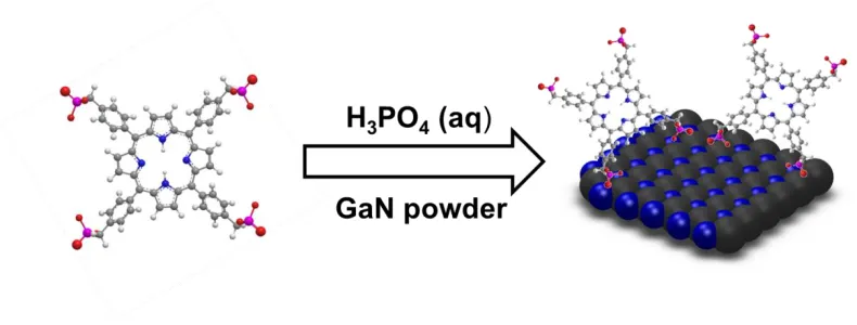
This work focused on the modification of milled GaN powder. Successful attachment of a porphyrin derivative to a GaN powder was performed via in-situ functionalization in the presence of phosphoric acid. The GaN powder was imaged using scanning electron
microscopy and was found to be heterogeneous in nature, adopting no consistent geometry in the aggregates. The aqueous stability of the porphyrin used was observed in deionized water and a solution of phosphoric acid using ultra-violet-visible spectroscopy. Surface chemistry was characterized with x-ray photoelectron spectroscopy and infrared spectroscopy, which identified evidence of successful functionalization through the presence of characteristic peaks. The interface stability of the covalent bond between GaN and porphyrin was evaluated using fluorescence spectroscopy and demonstrated no leaching of dye in water solutions for 20 days.
2.2 Introduction
18 with a band gap of 3.4 eV, is of significant interest.4 The surface modification of GaN has been used to develop field effect transistors with a myriad of surface treatments such as recognition peptides42, attached thiols7, alkyl groups9, DNA binders such as olefins8, 1-alkenes11, atomic layer deposition (ALD) thin films5 and alkylphosphonic acids10 for unique properties. The chemisorption of multiple molecules (haloanilines,43 aniline,44 pyrroline,45 water,46 and fluorine47) on GaN surfaces has traditionally been studied within controlled environments. Of the properties altered with surface chemistry, the modulation of optical properties of GaN is well documented48 and remains a continuing endeavor. The rise in applications of functionalized gallium nitride is attributed to their documented chemical inertness49 and biocompatibility through aqueous stability50 when compared to other III-V semiconductors. Recent work has shown that wet etching gallium nitride with phosphoric acid in the presence of adsorbates alters the surface morphology as well as the surface chemical composition.51 This combined process opens up the ability to change the semiconductor surface, which introduces opportunities for the development of functional interfaces as well as biosensing applications.
The attachment of dye molecules to semiconductor interfaces is beneficial for applications such as dye-sensitized solar cells (DSSC) and optical sensors.52 In DSSCs, the dye is crucial as it allows a wider bandwidth of light to be absorbed. Previous research has documented evidence that porphyrin sensitizers provide high photon-to-electron conversion efficiency.53 The most studied semiconductor in DSSCs so far is TiO2. Due to TiO2 having a
19 ZnO;24 however, the instability of the surface interaction between the dye and semiconductor is cited for the recorded low conversion efficiency. Recent use of GaN for DSSC applications has shown promise compared to transition metal oxides.54 Incorporating GaN in DSSCs provides a semiconductor with higher electron mobility than traditional TiO2. Additionally,
the high chemical stability of GaN under different environmental conditions and various solvents is beneficial for future solar cell devices.55
20 attachment. The stability of the attachment of the dye to GaN is important to assess since it is directly related to device efficiency.49 Fluorescence spectroscopy tracked the presence and possible leaching of dye from the powder after immersion in aqueous solutions for up to 20 days.
2.3 Materials and Methods 2.3.1 Powder Functionalization
The gallium nitride powder was obtained from Sigma-Aldrich (99.99 % trace metals basis) without pre-treatment. The powder was washed three times with acetone (Fisher Scientific) and three times with methanol (Sigma Aldrich). The samples were then rinsed with hydrochloric acid (Sigma Aldrich, 35-38 vole %) three times followed by three washes with deionized (DI) water (18.2 MΩ*cm).
A 7.125 μM solution of meso-tetra(4-phosphonomethylphenyl) porphine tetrasodium salt (TTP-PO3) (Frontier Scientific) with DI water was prepared. This solution was added in
a 1:1 (v:v) ratio to phosphoric acid (Fisher Scientific, 95%). The resulting solution was added to the washed and treated GaN powder and heated for a period of 120 minutes at 40°C. The powder was stirred throughout the duration of the treatment. A separate batch of powder was washed and stirred in phosphoric acid etchant only for the same time and under the same conditions. After 120 minutes, the GaN powder was washed with DI water three times and left overnight in a desiccator to dry.
2.3.2 Characterization
21 solution of 50 vol.% 7.125 μM TTP-PO3 and 50 vol.% phosphoric acid were tested. All
spectra were collected in quartz cuvettes.
Pre-treatment GaN powder was imaged with a JEOL 6010 LE SEM with an accelerating voltage of 20kV. The working distance for the image was 10 mm with a spot size of 50. A magnification of 3,000x was used to take the micrograph. The IR data was gathered with a Bruker 1 95 9670 ALPHA Fourier-Transform-Infrared Spectrometer (FT-IR) equipped with a KBr beam splitter. Using the instrument OPUS software, the resolution was set to 2 cm-1 for all scans. The samples were evaluated by averaging 36 scans in transmittance mode. All semiconductor samples were prepared using 50 grams of KBr to 1 gram of GaN powder. For the TTP-PO3 data collection 100 grams of KBr to 0.1 gram of TTP-PO3 was
utilized. The OPUS software was employed to perform a background subtraction and smooth line profiles.
All XPS evaluation was performed on an Axis Ultra XPS manufactured by Kratos. The X-ray source was a monochromated Al Kα with beam energy of 1486.7. eV. A charge neutralizer was used with 2.0 A filament current to account for charging of the samples. The pressure was maintained within the sample chamber to 3 x 10⁻⁸ Torr. The samples were mounted onto an aluminum sliding sample holder using adhesive coated copper tape. For each sample, a survey scan was collected using a sweep pass energy of 160 eV. High
22 eV. A Lorentzian fit was used to constrain the full width half-maximum of the deconvoluted peaks to the primary peaks. A second calibration was performed to adjust for the high degree of charging evident in the N 1s region scan. The N-Ga peaks for each sample was calibrated to 397.3 eV.58
The fluorescence data was obtained with an excitation wavelength of 455 nm at maximum LED source intensity. The sample was sonicated before testing to ensure
dispersion of particles within the solution. All data was plotted and analyzed with Origin 9.0. 2.4 Results and Discussion
2.4.1 In-Situ Functionalization of GaN Powder with Porphyrin
Porphyrin molecules show promise for sensitization due to their reported high conversion efficiencies.59 Stable bonding between the semiconductor and dye molecules is critical for stability and optimal electronic properties in photonic devices, which has been explored by a number of research groups. Brennan et al. investigated various anchoring groups for attaching porphyrin molecules to semiconductor surfaces.60 The use of porphyrin dyes to successfully sensitize TiO2 was described by Odobel et al.53 In this study, we
performed an in-situ functionalization of GaN powder with a porphyrin derivative TTP-PO3
using a recently reported in situ approach.1 The covalent attachment of the porphyrin to the GaN was investigated to determine success and stability of the reaction.
23 porphyrin was needed in order to be compatible with phosphoric acid used during the in situ procedure. The TTP-PO3 salt provides a water-soluble molecule containing phosphonate side
groups available for attachment through a bidentate mode. In future studies of porphyrin dye attachment to GaN, the incorporation of a metal center within the molecule will be explored.
Prior to the functionalization method displayed in Figure 2.1 the GaN powder was washed with various solvents and treated with hydrochloric acid. The hydrochloric acid was used to remove the native thin oxide layer which forms on the GaN during storage under normal room temperature and humidity environmental conditions. During functionalization, H3PO4 serves as an etchant that encourages the formation of a controlled oxide layer in
addition to removing nitrogen rich regions from the surface. By adding TTP-PO3 while
etching, phosphonic groups preferentially bind to metal rich areas on the surface as well as to protonated and hydroxyl terminated regions. This in turn provides a binding site for TTP-PO3
as well as caps existing gallium oxide to hinder dissolution in water. The 7.125 μM solution of TTP-PO3 used in this study falls within the concentrations ranges that other surface
24 both testing successful functionalization as well as quantification of the stability of the dye attachment to the GaN interface.
Figure 2.1. Schematic diagram of the in situ functionalization process showing bidentate binding of the porphyrin on the surface of the GaN powder.
2.4.2 Stability of Porphyrin in Phosphoric Acid
An important consideration in this study was the possible aggregation or degradation of TTP-PO3 in solution, DI water, or with phosphoric acid. In a typical UV-Vis absorbance
spectrum, a sharp Q band is used to provide evidence of the monomeric species of TTP-PO3.
If aggregation occurs, this peak will blue-shift as well as broaden in the UV-Vis spectrum. In Figure 2.2, no aggregation or degradation was observed in TTP-PO3 dissolved in water or
mixed with phosphoric acid etching solution. The solutions were left for 4 hours before they were tested to allow enough time for aggregates to form. These results provided evidence that TTP-PO3 was compatible with the solution conditions necessary for the in situ method of
25 Figure 2.2. Room temperature UV-Vis spectra of (a) 7.125 μM TTP-PO3 in DI water and (b)
50% 7.125 μM TTP-PO3 in DI water and 50% phosphoric acid.
2.4.3 Morphological Characterization by SEM
SEM quantified the homogeneity of the GaN powder. Images, such as those seen in Figure 2.3, show that the aggregate size of the GaN powder varies widely and the overall surface holds little homogeneity. SEM was also used to probe for evidence of aggregation of organic contamination and TTP-PO3. We observed that the powder was free of organic
particulates from environmental contamination. The overall aggregate size was recorded to be dissimilar in various batches and ranged from less than 1 μm up to sizes greater than 5
μm. For this study, uniformity of the particulates making up the powder was not a concern as
26 Figure 2.3. SEM image of GaN powder showing the size and heterogeneity of aggregrates within the powder. Scale bar is 5 μm.
2.5 Surface Characterization
2.5.1 X-Ray Photoelectron Spectroscopy
XPS was utilized to confirm successful attachment of TTP-PO3 to the GaN powder.
Multiple survey and high-resolution regional scans were collected following cleaning, etching, and functionalization. In the samples that underwent etching, the presence of a P 2p peak was expected due to residual phosphonic acid groups on the surface. The collection of C 1s spectra provides a calibration technique as well as probing mechanism into TTP-PO3.62
However, the adventitious carbon peak lies in close proximity with the expected peak for the porphyrin (285.0 eV). The Ga 2p region was collected to determine the presence of specific gallium species on the surface. These regional scans offer evidence of oxide species, Ga2O3
27 A peak centered near 1120 eV was present in the survey scan for each of the samples. This peak was attributed to gallium content from both the powder and surface oxide seen within the Ga 2p spectra. Another peak near 530 eV, again recorded in the survey scans for all three types of samples, indicates the presence of oxide groups on the surface as seen from the O 1s region. In accordance with the identification of gallium, the peak centered near 400 eV confirmed presence of nitrogen, which is as expected and was observed within the high resolution N 1s spectra. A peak centered near 135 eV was present for the etched only GaN powder, as well as the etched and functionalized GaN powder, which was distinctly absent for the cleaned powder. This peak was attributed to P 2p as a result of etching and
functionalization. For all three types of samples, carbon contamination was present and verified due to the emergence of a peak centered at 284.8 eV.
The high-resolution regional scan of Ga 2p was used to determine the nature of the gallium species on the surface of the samples. The Ga 2p spectra is preferred over the Ga 3d spectra for high resolution scans for its lower kinetic energy of radiation, therefore providing higher surface sensitivity.63 Casa XPS was used to analyze and fit the data. For all three samples, a peak was present and centered near 1118 eV which was attributed to the Ga-N bonding expected on the surface.64 Each sample contained a species centered near 1116 eV which was due to Ga-Ga bonding near the surface.65 The species present for each sample near 1119.75 eV was attributed to Ga2O3.64 The existence of sub oxide species such as Ga2O,
28 Figure 2.4. Ga 2p regional XPS spectra of (a) clean GaN powder, (b) clean, etched GaN powder, and (c) functionalized GaN powder.
The ratio of gallium species recorded in the spectra provided information about the nature of the gallium on the surface of the samples. In the clean GaN powder the presence of sub oxide species was not evident from the data. The percent area of Ga2O3 in the Ga 2p peak
of the clean GaN powder was 11.43% and the percent area of Ga-N was 82.08%. In the etched only sample of GaN sub oxide species were a significant portion of the peak. The percent area of Ga2O3 was 20.12%, of sub oxides was 67.51% and of Ga-N was 8.69%. In
the functionalized samples of GaN powder the percent area of Ga2O3 was 20.69%, of sub
oxide species was 45.46% and of Ga-N was 31.11%. As expected, the etching process shows evidence of the production of oxide and sub oxide species in the GaN powder samples that were used.
29 two species contributing to this peak was evident. The species with the lowest binding energy was attributed to adventitious carbon and was calibrated to 284.8 eV.66 The atmospheric contamination of samples with hydrocarbon molecules was evident due to the C 1s spectra. The presence of a species near 286 eV in the fitted peak can be contributed to the C-N bond present in the porphyrin.63 Due to the powder nature of the samples, the ability to distinguish between peaks in this region was difficult.
Figure 2.5. C 1s regional XPS spectra of (a) clean GaN powder, (b) clean, etched GaN powder, and (c) functionalized GaN powder.
30 clean GaN powder showed no peak in the P 2p high resolution scan and both the etched and functionalized powder samples exhibited peaks in this region.
Figure 2.6. P 2p regional XPS spectra of (a) clean GaN powder, (b) clean, etch GaN powder, and (c) functionalized GaN powder.
31 that is attributed to N-Ga bonding was used for calibration because it is present in all
samples. This peak is present close to 397 eV and was calibrated to 397.3 eV to account for the charging.58 The spectra of all three samples are shown in Figure 2.4. Due to the Al Kα source used with the XPS instrument, there was an overlap between the Auger peaks of the Ga and the N 1s peaks. The Ga Auger peaks (LMM 1 and LMM 2) were present at lower binding energy than the N-Ga peak for each sample, around 395.4 and 392.1 eV. The functionalized sample contained a species centered near 400.8 eV, which was not present in any of the other samples. The presence of the amine groups found on the TTP-PO3
contributes to this peak and provides evidence that the GaN was successfully modified with the porphyrin derivative.
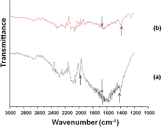
32 2.5.2 Infrared Spectroscopy
FT-IR signatures of GaN powders have been studied by a number of research groups. For example, Baraton and Gonsalves investigated the infrared spectra of both aluminum and gallium nitride for nanostructured powders.69 The synthesis of GaN nanowires was
successfully accomplished by Wei and Shi, and evidence for this was gathered by FT-IR.70 Shi and Xue obtained FT-IR spectra for the determination of suitable growth conditions for GaN nanowires.71 This prior work has presented evidence of two strong peaks near 560 cm-1 and 610 cm-1. The band at 560 cm-1 is attributed to the bond between gallium and nitrogen stretching in the material.71
Prior work on nanostructured GaN demonstrated high levels of uniformity and homogeneity. The samples in this study possess low homogeneity due the milling method utilized for their preparation. Xiao et al. examined GaN powders72 and reported a broad peak located between 500 and 700 cm-1 and discussed its varied position following different treatment temperatures. A second, smaller peak was found near 1630 cm-1 that corresponded to GaN powder. A third, medium sized peak resided near 3410 or 3420 cm-1,the location of which depended on experimental parameters. The complexities involved in determining specific peak assignments for GaN have been previously examined in the literature.69 Additionally, a broad peak near 2100 cm-1 was assigned to Ga-H due to a nitrogen vacancy previously discussed by others.73
33 molecules by Ogoshi et al.74 reported theoretically calculated FT-IR peaks and assigned them based on the stretching or bending modes of the molecules. Santiago et al. gathered FT-IR data between 1800 and 400 cm-1 for an iron porphyrin under various pH conditions.75 The spectra contain various common species at expected wavenumbers including large peaks near 1650 cm-1 and 1000 cm-1. The peak near 1000 cm-1 was attributed to the stretching mode the P-O bond. A peak present near 1650 cm-1 was attributed to the stretching modes of the bond between the ring structure carbons and nitrogen within the porphyrin.74 Brennan et al. performed various spectroscopy techniques to compare functional groups for porphyrin attachment to TiO2.60 The FT-IR spectra that were obtained for the iron porphyrin under
different pH environments showed the same peaks hear 1650 and 1000 cm-1.
34 Figure 2.8. FTIR regional scan between 3000 and 1200 cm-1 of KBr mixed with (a)
functionalized powder and (b) TTP-PO3.
2.5.3 Stability Testing Using Fluorescence Spectroscopy
By utilizing a porphyrin adsorbate, the naturally strong fluorescent signal can be used to confirm successful functionalization both pre and post soaking following the in situ procedure. The fluorescence spectra of porphyrin molecules have been well studied in previous literature. Typically, porphyrin molecules possess distinct Soret bands near 430 nm as well as two Q-band peaks near 550 and 590 nm. 60 Emission peaks are expected near 620 and 670 nm as well. The spectral sweep used in this work started at 550 nm and moved to higher wavelengths, meaning the useful peaks which would be expected to be present and easily observed would be the emission peaks near 620 and 670 nm.
35 investigating the presence of the porphyrin in other solutions. In order to investigate and compare this to the fluorescence of the functionalized sample, it was mixed with DI water and sonicated in order to disperse the powder particles of the sample. The two spectra were compared and expected to possess the same signature peaks. The difference in concentration of the two solutions as well as the nature of the solution (loose modified GaN powder vs. dissolved porphyrin molecules) accounts for changes in intensity of the characteristic peaks. A small peak centered near 610 nm was seen in the shadow of an overwhelming peak at 690 nm for TTP-PO3 in water. The spectrum of the sonicated solution of the modified GaN
powder showed peaks in the expected positions supporting the notion of successful functionalization of the semiconductor surface.
A sample of the functionalized powder was left under ambient temperature and humidity in DI water for a period of 20 days to test for any possible porphyrin leaching in solution. The degree of stability was assessed by measuring the amount of any porphyrin dissolved in the water solution. We note that the powder exhibited the same characteristics shown in Figure 2.6 (b) even after the water soak. The soaking solution containing the functionalized powder was centrifuged in order to separate the particulates. Presence of leached TTP-PO3 into solution would produce the characteristic porphyrin signature. The
spectrum of the soaking solution shows no peaks at the expected wavelengths of 610 and 690 nm as seen in Figure 2.6 (c). The absence of these peaks supports the assessment that TTP-PO3 did not desorb from the GaN surface and dissolve into the water solution. This, in turn,
36 Figure 2.9. Fluorescence spectroscopy spectra of (a) 7.125 μM solution of TTP-PO3 in DI
water, (b) sonicated solution of functionalized powder in DI water, and (c) wash of functionalized powder in DI water after 20 days.
2.6 Conclusion
In conclusion, the attachment of a porphyrin derivative to GaN powder was
performed using an in-situ functionalization procedure. XPS analysis confirmed the existence of amine groups on the modified GaN powder. The presence of C-N and C=N peaks in the FT-IR spectrum of the functionalized powder provided further evidence for the attachment of the porphyrin to the semiconductor surface. The stability of the bound porphyrin to the GaN interface was tested for a period of 20 days in water solution. No desorbed porphyrin was detected after the soaking period. We attribute this stability in solution to the covalent attachment of the porphyrin to the GaN powder surface. Future studies will focus on
37 3. In-situ and Ex-situ Functionalization of Nanostructured Gallium Oxyhydroxide with a Porphyrin Dye
Brady L. Pearce, 1 Nora G. Berg,1 Matthew S. Rahn,2 Albena Ivanisevic1*
1
Department of Materials Science and Engineering, North Carolina State University, Raleigh, North Carolina, 27695, USA
2
Department of Materials Science and Engineering, Pennsylvania State University, State College, Pennsylvania, 16801, USA
3.1 Abstract
The surface attachment of a porphyrin dye to nanocrystalline GaOOH was performed using two routes of solution based functionalization. The first method of functionalization utilized an in-situ incorporation of dissolved porphyrin salt in solution during the microwave synthesis step. Additionally, synthesized GaOOH nanorods were mixed in porphyrin solution after the microwave process to make an ex-situ GaOOH/TTP-PO3. X-Ray
Photoelectron Spectroscopy confirmed the presence of expected surface species and provided evidence of increased surface coverage of TTP-PO3 on GaOOH in the ex-situ
GaOOH/TTP-PO3 as compared to the in-situ one. Size and morphology changes were investigated using
SEM and, along with analysis of XRD, the in-situ samples showed larger crystallite sizes. This was confirmed with PL due to the higher bandgap energy evident in the ex-situ GaOOH/TTP-PO3 compared to the in-situ sample. A stability study was performed using
GaOOH/TTP-38 PO3 sample. The stability of the in-situ GaOOH/TTP-PO3 makes it attractive for a number of
interfacial applications. 3.2 Introduction
The use of wide bandgap semiconductor materials as optoelectronic platforms for attaching functional organic molecules shows great promise for various applications ranging from biomedical to green energy.76 Gallium oxyhydroxide (GaOOH) is an inorganic material with a bandgap of 4.75 eV. GaOOH is of particular interest for semiconductor research due to its nature as a precursor for both gallium oxide13 (Ga2O3) and gallium nitride (GaN).14
Performing solution based functionalization of GaOOH with phosphonic side group containing molecules is inherently simple due to the surface oxide layers present in the material. The surface attachment of dye molecules to wide bandgap semiconductors can potentially find applications in solar cell research including dye-sensitized solar cells (DSSCs)26 as well as imaging and biosensing. A substantial amount of research has focused on the use of several wide bandgap materials such as TiO221and ZnO.77 There is a need for
exploring alternative wide bandgap semiconductors with higher electron mobility than TiO226
and better interfacial stability than ZnO.78
Nanostructured materials are especially attractive for surface functionalization due to the high surface area available for the immobilization of organic molecules.21 The high surface area to volume ratio also is useful in enabling high photocatalytic activity of the nanostructured material.79 Ga2O3 nanowires have been functionalized for sensing
atmospheric hydrocarbons.80 Nanoribbons of β-Ga2O3 with various adsorbed organics were
39 The functionalization of Ga2O3 nanowires with pyruvic acid was studied for
capacitance-based gas sensing.82
The fabrication of GaOOH nanostructures has been investigated using various methods and precursor materials. Using gallium nitrate (Ga(NO3)3) and various additives, a
microwave-assisted method has been used to form GaOOH nanorods,83 along with a hydrolysis method in the presence of lanthanide ions84 and a calcination reaction with sodium carbonate.85 Ga(NO3)3 was also utilized with a sodium hydroxide (NaOH) titration and
hydrothermal treatment to form GaOOH nanostructures,86 with a sodium doceyl benzene sulfonate surfactant87 and in the presence of no surfactant.88 Hydrothermal treatment of GaCl3 in the presence of urea was performed to make various nanostructured GaOOH
crystals with diamond-like cross sections89 and ultrasound radiation sonication on GaCl390 in
a benzene saturated solution91 produced GaOOH nanostructures. The growth of α-GaOOH as well as iron oxyhydroxide in various concentrations using an alkaline precipitation reaction has been reported.92 A high pressure phase, β-GaOOH, was synthesized using a high-pressure chamber.93 The synthesis of GaOOH nanorods from ball-milled GaN powders was done to make GaOOH particles ranging in size from 10 to 80 nm.94 Room temperature synthesis of GaOOH nanostructures was accomplished by Kisailus et al.95 To the best of knowledge, no prior studies have attempted to modify the nanostructured inorganic material with organic adsorbates in solution.
40 characterization techniques provided a comparison between the two functionalization methods. The microwave synthesis technique96 was chosen due to the ease of preparation using solutions with just DI water and the reactants. X-Ray Diffraction (XRD) scans were evaluated to assess the crystallinity of the product after various processing techniques. The morphological properties of the nanostructures were investigated using Scanning Electron Microscopy (SEM). Photoluminescence (PL) Spectroscopy was used to investigate the effect of the presence of the dye on the luminescent properties of GaOOH. The properties of the interface between the dye and semiconductor were investigated with XPS and the stability of the functionalized nanostructured materials was tested using Fluorescence Spectroscopy. 3.3 Materials and Methods
3.3.1 Microwave Synthesis and Functionalization
The gallium nitrate hydrate powder and sodium hydroxide were obtained from Sigma Aldrich. Solutions of 0.1 M Ga(NO3)3 and 5 M NaOH were made with deionized (DI) water
(18.2 MΩ*cm). The NaOH solution was added drop wise to the Ga(NO3)3 solution until a pH
of 8 was reached. The resultant solution was placed in a CEM Discover LabMate microwave reaction vessel. The instrument was set to a maximum power of 200 W, the temperature was set to 120˚C and the reaction was programmed to run for 20 minutes. Prior to being left overnight to dry in an oven, the samples were washed with DI water and filtered. One sample was placed in the oven without performing the DI wash or filtration step.
The in-situ GaOOH/TTP-PO3 samples were synthesized using the same procedure
except the Ga(NO3)3 was added to a solution of 7.125 µM
41 water before the drop wise titration with NaOH. To produce the ex-situ GaOOH/TTP-PO3,
some of the filtered GaOOH product was added to a solution of 7.125 µM TTP-PO3 in a
centrifuge tube and left mixing on a rocking platform for 24 hours. The resulting product was washed with DI water and filtered and left to dry overnight in a dessicator.
3.3.2 Characterization
The SEM used was a FEI Verios 460L Field Emission SEM. The detector on the instrument was a concentric higher energy electron detector for each of the images taken. The clean GaOOH sample was imaged at a working distance of 6.1 mm with a stage bias of 1500 V. The current was set to 50 pA and the voltage was 2.00 kV. The ex-situ GaOOH/TTP-PO3 was imaged at a working distance of 7.0 mm with a stage bias of 1200 V.
The current was set to 0.20 nA with a voltage of 2.00 kV. The ex-situ GaOOH/TTP-PO3 was
imaged at a working distance of 6.8 mm with a stage bias of 1300 V. The current was set to 50 pA and the voltage was 2.00 kV.
XRD analysis was done using a Rigaku SmartLab X-Ray Diffractometer. A Cu Kα x-ray source was used with a voltage of 40 kV and a current of 44 mA. The powder diffraction was done with Bragg-Brentano optics. All scans were collected from 2 of 10 degrees to 80 degrees. A step size of 0.05 degrees was utilized for a scan time of 2 seconds and a resolution of 0.0002.
42 The samples contained in the quartz cuvettes were mounted on the optical table. A UV enhanced CCD connected to a fiber optic cable was used as a detector to collect data. Analysis and acquisition of the data was performed using LightField software, manufactured by Princeton Instruments. The data was normalized and analyzed using Orgin 9.0 to determine peak positions.
The XPS data was obtained with a Kratos Analytical Axis Ultra XPS. A monochromated Al Kα (energy of 1486.7 eV) X-ray source was employed in all characterization with a 2.0 A filament charge neutralizer in order to reduce the effects of charging. The sample chamber pressure was maintained at 3.0 x 10⁻⁸ Torr. All samples were mounted to an aluminum sliding sample holder with double sided copper tape. A survey scan was collected for each of the samples with a pass energy of 160 eV. High resolution regional scans of C 1s, O 1s, Na 1s, P 2p, Ga 2p, Ga 3d and N 1s were obtained with a pass energy of 20 eV. Casa XPS Version 2.3.12.8 was utilized to fit the peaks and determine atomic percentages of each sample from the survey scans. Background subtraction was done using a Shirely approximation and all peaks were calibrated by setting the adventitious carbon C 1s peak to 284.8 eV. The full width at half-maximum of the deconvoluted peaks was constrained to the primary peaks using a Lorentzian fit.
43 3.4. Results and Discussion
3.4.1 Synthesis and Functionalization with Porphyrin Dye
The method of using microwave synthesis96 to produce GaOOH nanorods was chosen over an autoclave technique97 due to the ease of preparation with DI water as the only solvent. The porphyrin dye TTP-PO3 was chosen for functionalization because of its water
solubility as well as the assumption that the phosphonic groups provided a means of attachment to surface oxides for increased stability. The possible mechanism of GaOOH nanorod formation from Ga3+ ions in the presence of water has been explored. There exist many possible chemical routes for GaOOH nanorod synthesis, dependent on the precursor ion, as well as a mechanism which relies on metallic Ga.90 The following reaction was described by Avivi et al.90
Ga3+ + 2 H2O ↔ GaOOH + 3 H+
The synthesized GaOOH material was white with a flake like consistency following the filtration and drying process. The SEM image of the clean GaOOH is displayed in Figure 3.1(a). The GaOOH is heterogeneous in nature with both nanorod like features as well as other nanocrystallite particles. The nanocrystallite and nanorod structures varied in size with the lengths of the nanorods being from around 40 nm to as large as 100 nm. The nanorods that were formed did not seem to have a preferred direction and were randomly ordered in the sample.
44 stability and the effect of the functionalization on the properties of the semiconductor. The use of porphyrin as a sensitizing agent for semiconductors was explored by Brennan et al.60 Porphyrin dye was used to produce a DSSC with TiO2 with a conversion efficiency of 3%.59
In previous work with solution based functionalization on GaN, an etchant was required to produce a controlled oxide layer for phosphonic group attachment.1 A particular advantage of the sensitization of GaOOH is the native presence of this oxide layer so no additional and harmful etchant is required to attach a soluble dye to the semiconductor surface.
The inclusion of TTP-PO3 with the GaOOH nanorods in this work was done through
two different methods to compare and contrast the various property modifications that occurred. The first functionalization method that was followed was a simple soaking procedure after the microwave synthesis of the nanostructured GaOOH. This sample is referred to as ex-situ due to it being processed outside of the original reaction. The samples were filtered to remove any unreacted nitrate then left rocking overnight in a solution of DI water and porphyrin. The native oxide layer present on the GaOOH provided a means of attachment for the phosphonic groups on the porphyrin dye. The resulting solid solution was filtered and dried and after this was a vibrant green color (Figure 2).
SEM images of the ex-situ GaOOH/TTP-PO3 samples were inspected to determine
45 nanocrystallites, suggesting a simple adsorption of the TTP-PO3 onto the GaOOH
nanocrystalites.
Figure 3.1. SEM images of (a) clean GaOOH nanorods, (b) ex-situ GaOOH/TTP-PO3 and (c)
in-situ GaOOH-TTP/PO3.
In order to facilitate an even simpler, faster and more environmentally friendly approach, the second method was a one-step solution based in-situ functionalization and synthesis. Along with the precursor materials Ga(NO3)3 and NaOH, the TTP-PO3 was added
to the reaction mixture. The remaining solid product from the microwave process was washed with DI water, filtered and dried overnight. The solid was a pale yellow color and resembled the flake like structure of the clean GaOOH. The following is a modification of the original chemical equation to account for the presence of porphyrin.
Ga3+ + 2 H2O + TTP-PO3 ↔ GaOOH/TTP-PO3 + 3 H+
An SEM image was obtained to explore the effect the presence of TTP-PO3 had on