Simulation of SEPIC-CHMLI based micro
inverter for high step-up voltage conversion
M.Ram kumar
1, I.Sayed mohammed
2, J.Manikanda prashath
3P.G. Student, Department of Electrical Engineering, PSNA Engineering College, Dindigul, Tamilnadu, India1
Assistant Professor, Department of Elecrical Engineering, PSNA Engineering College, Dindigul, Tamilnadu, India2
U.G. Student, Department of Electrical Engineering, PSNA Engineering College, Dindigul, Tamilnadu, India3
Abstract:Within the photovoltaic power-generation market, the ac PV module has shown obvious growth. This paper proposes an implementation of Single Ended Primary Inductor (SEPIC) converter and cascaded multi level inverter for an AC load using Photovoltaic energy as a source. This paper proposes a converter that employs a continuous-conduction-mode SEPIC converter with low reverse-recovery loss. To convert the boosted DC output voltage from PV module into AC, a cascaded multi level inverter with multi carrier pulse width modulation is implemented. An operation principle and a detailed analysis of the proposed converter are presented. A 12V input voltage, (220-230)V output voltage of the proposed converter has been implemented. The simulation work of these SEPIC converter and cascaded multi level inverter fed RL load have been done using MATLAB software.
Keywords:PV cell, SEPIC converter, cascade multilevel inverter, multi carrier PWM
I. INTRODUCTION
Thephotovoltaic energy system has the advantages of absence of fuel cost, no environmental impacts, low maintenance and lack of noise and also it is a kind of renewable energy system. So it is becoming popular in the recent years, as a resource of energy. Modelling and simulation of PV array based on circuit model and a mathematical equation is proposed [9]. As the photovoltaic (PV) cell exhibits the nonlinear behaviour, while matching the load to the photovoltaic modules, DC-DC power converters are needed. There are several converter configurations such as Buck, Boost, Buck-Boost, SEPIC, ĆUK, Fly-back, etc. Buck and Boost configurations can decrease and increase the output voltages respectively, while the others can do both functions. Buck, Boost, Buck Boost converters as interface circuits are proposed and analyzed in [6]. CUK and SEPIC converters are analyzed in [1,7].the SEPIC converter should operate with high switching frequency. However, as the switching frequency increases, the reverse recovery current of the output diode affects the switching devices in the form of additional switching losses. Other adverse effects of the reverse-recovery problem include electromagnetic interference (EMI) noises and additional thermal management. Also, the switch utilisation factor in the SEPIC converter is much lower than that of other topologies, such as the buck and boost converters. In other words, the power-handling capabilities of the semiconductor devices in the SEPIC converter are much lower than those of the buck or the boost converter at the same power level. Thus, the reduction of reverse-recovery loss is particularly important for the SEPIC converter.
Different topologies MLIs for the conversion from DC to AC are available such as Neutral point clamped MLI (NPC-MLI), Flying capacitor MLI (FC-MLI), Cascade Bridge MLI (CHB-MLI) and Asymmetrical Cascade H-Bridge Multilevel inverters. Among them MLIs are mostly used for PV applications because each cell of CHB-MLI requires separate DC sources which can be easily supplied by individual PV arrays and each H-Bridge cell will be available in a single module6. The number of levels of the output wave form increased by cascading the no. of H-Bridge cells. There is a large no. of control techniques developed so far to control the operation of multilevel inverters such as SVPWM, SPWM, OHPWM, SHE-PWM, Hybrid modulation.
AC output voltage of desired magnitude and frequency. To drive the AC load, the output dc voltage of SEPIC converter is converted into AC by means ofcascade multilevel inverter.In this paper PV source fed AC load is proposed with SEPIC converter and cascade multilevel inverter as interface circuits. Multi carrier pulse width modulation technique is employed for the control of cascade multilevel inverter. The overall block diagram is shown in Fig.1
Fig.1 Over all block diagram
II. ANALYSISOFSEPICCONVERTERANDPVCELL
PV system directly converts sunlight into electricity. The basic device of a PV system is the PV cell. Cells may be gathered to form modules or arrays. More sophisticated applications require DC-DC converters to process the electricity from the PV device. These converters may be used to either increase or decrease the PV system voltage at the load. The proposed SEPIC converter operates in boost mode.
A. PV Module Characteristics:
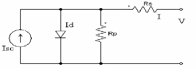
The practical equivalent circuit of a PV module is shown in Fig.2
Fig. 2 Equivalent circuit of a PV module
In the equivalent circuit, the current source represents the current generated by light photons and its output is constant under constant temperature and constant irradiance. The diode shunted with the current source determines the I-V characteristics of PV module. There is a series of resistance in a current path through the semiconductor material, the metal grid, contacts, and a current collecting bus. These resistive losses are lumped together as a series resistor (Rs). Its effect becomes very noteworthy in a PV module.
The loss associated with a small leakage of current through a resistive path in parallel with the intrinsic device is represented by a parallel resistor (Rp). Its effect is much less noteworthy in a PV module compared to the series resistance, and it will only become noticeable when a number of PV modules are connected in parallel for a larger system. The characteristic equation which represents the I-V characteristic of a practical photovoltaic module is given
PV module
SEPIC Converter
Cascade Multilevel Inverter
AC Load
Where I and V are the PV cell current and voltage respectively, IPV is the photovoltaic current, Io is the reverse saturation current of diode, Vt= Ns*kT/q is the thermal voltage of the array with Ns cells connected in series, k is the Boltzmann constant (1.3806*10-23J/K), T is the temperature of the p-n junction, q is the electron charge and n is the diode is constant. 𝐼𝑃𝑉and𝐼𝑂 are given as follows
𝐼𝑝𝑣 = { 1 + 𝑎 𝑇 − 𝑇𝑟𝑒𝑓 𝐼𝑠𝑐
𝐺
1000 (2)
𝐼 = 𝐼𝑜 𝑇𝑟𝑒𝑓 (3)
Where “a” is temperature coefficient of 𝐼𝑠𝑐, G is the given irradiance in W/m2 and Egis the band gap energy (1.16eV for Si)
A. Design of SEPIC Converter:
1) Introduction:
Using a coupled inductor takes up less space on the PCB and tends to be lower cost than two separate inductors. The capacitor Cs isolates the input from the output and provides protection against a shorted load.
L1
Cin Q1
C1
L1 D1
Cout Vout Vin
Fig.3 SEPIC Topology
L1
Cin
C1
L1 Cout
Vout Vin
+
-I L2 +
L1
Cin
Cs
L1 D1
Cout Vout Vin
I L1
IL 2
+
-+
-Fig.4 SEPIC Converter Current Flow
Top: During Q1 On-Time, Bottom: During Q1 Off-Time
2) Duty Cycle Consideration:
For a SEPIC converter operating in a continuous conduction mode(CCM),the duty cycle is given by:
𝐷𝑢𝑡𝑦 𝑐𝑦𝑐𝑙𝑒 𝐷 = 𝑉𝑜𝑢𝑡 + 𝑉𝐷 𝑉𝑖𝑛 + 𝑉𝑜𝑢𝑡+ 𝑉𝐷 (4)
𝑉
𝐷is the forward voltage drop of the diode𝐷
1.The maximum duty cycle is given by𝐷𝑚𝑎𝑥 = 𝑉𝑜𝑢𝑡 + 𝑉𝐷 𝑉𝑖𝑛 (𝑚𝑖𝑛 )+ 𝑉𝑜𝑢𝑡 + 𝑉𝐷 5
3) Inductor Selection:
A good rule for determining the inductance is to allow the peak-to-peak ripple current to be approximately 40% of the maximum input current at the minimum input voltage. The ripple current flowing in equal value inductors L1 and L2 is given by:
∆𝐼𝐿= 𝐼𝑖𝑛 × 40% =
𝐼𝑜𝑢𝑡 × 𝑉𝑜𝑢𝑡
𝑉𝑖𝑛 (min )
× 40% (6)
The inductor value is calculated by:
𝐿1 = 𝐿2 = 𝐿 = 𝑉𝑖𝑛 (min ) ∆𝐼𝐿× 𝑓𝑠𝑤
× 𝐷(max ) (7)
Where,𝑓𝑠𝑤 is the switching frequency and 𝐷(max ) is the duty cycle at the minimum. The peak current in the inductor, to ensure the inductor does not saturate, is given by:
𝐼𝐿1(𝑝𝑒𝑎𝑘 )= 𝐼𝑜𝑢𝑡 ×
𝑉𝑜𝑢𝑡 × 𝑉𝐷
𝑉𝑖𝑛 (min )
× (1 + 40%/2) (8)
𝐼𝐿2(𝑝𝑒𝑎𝑘 )= 𝐼𝑜𝑢𝑡 × (1 + 40%/2) (9)
4) Power MOSFET Selection:
The parameters governing the selection of the MOSFET are the minimum threshold voltage V th (min), the on resistance RDS (ON), gate-drain charge QGD, and the maximum drain to source voltage, VDS(max). Logic level or sub logic-level threshold MOSFETs should be used based on the gate drive voltage. The peak switch voltage is equal to 𝑉𝑖𝑛+𝑉𝑜𝑢𝑡. The peak switch current is given by:
𝐼𝑄1(𝑝𝑒𝑎𝑘 )= 𝐼𝐿1(𝑝𝑒𝑎𝑘 )+ 𝐼𝐿2(𝑝𝑒𝑎𝑘 ) (11)
The RMS current through the switch is given by:
𝐼𝑄1(𝑟𝑚𝑠)= 𝐼𝑜𝑢𝑡
(𝑉𝑜𝑢𝑡+𝑉𝑖𝑛min +𝑉𝐷)×(𝑉𝑜𝑢𝑡+𝑉𝐷)
𝑉2𝑖𝑛min (12)
The MOSFET power dissipation 𝑃𝑄1 is approximately:
𝑃𝑄1 = 𝐼𝑄1𝑟𝑚𝑠 × 𝑅𝐷𝑆𝑂𝑁 × 𝐷𝑚𝑎𝑥+ 𝑉𝑖𝑛min + 𝑉𝑜𝑢𝑡 × 𝐼𝑄1𝑝𝑒𝑎𝑘 × 𝑄𝐺𝐷×𝑓𝑠𝑤
𝐼𝐺 (13)
𝑃𝑄1, the total power dissipation for MOSFETs includes conduction loss (as shown in the first term of the above equation) and switching loss as shown in the second term. IG is the gate drive current. The 𝑅𝐷𝑆𝑂𝑁 value should be selected at maximum operating junction temperature and is typically given in the MOSFET data sheet. Ensure that the conduction losses plus the switching losses do not exceed the package ratings or exceed the overall thermal budget.
5) Output Diode Selection:
The output diode must be selected to handle the peak current and the reverse voltage. In a SEPIC, the diode peak current is the same as the switch peak current IQ1(peak). The minimum peak reverse voltage the diode must withstand is:
𝑉𝑅𝐷1=𝑉𝑖𝑛 max + 𝑉𝑜𝑢𝑡 max (14)
Similar to the boost converter, the average diode current is equal to the output current. The power dissipation of the diode is equal to the output current multiplied by the forward voltage drop of the diode.Schottky diodes are recommended in order to minimize the efficiency loss.
6) SEPIC Coupling Capacitor Selection:
The selection of SEPIC capacitor, Cs, depends on the RMS current, which is given by:
𝐼𝐶𝑆 rms = 𝐼𝑜𝑢𝑡 ×
𝑉𝑜𝑢𝑡 + 𝑉𝐷
𝑉𝑖𝑛 (𝑚𝑖𝑛 )
(15)
The SEPIC capacitor must be rated for a large RMS current relative to the output power. This property makes the SEPIC much better suited to lower power applications where the RMS current through the capacitor is relatively small (relative to capacitor technology). The voltage rating of the SEPIC capacitor must be greater than the maximum input voltage. Tantalum and ceramic capacitors are the best choice for SMT, having high RMS current ratings relative to size. Electrolytic capacitors work well for through-hole applications where the size is not limited and they can accommodate the required RMS current rating. The peak-to-peak ripple voltage on𝐶𝑠 (assuming no ESR):
∆𝑉𝑐𝑠 =
𝐼𝑜𝑢𝑡 × 𝐷𝑚𝑎𝑥
𝐶𝑠× 𝑓𝑠𝑤
A capacitor that meets the RMS current requirement would mostly produce small ripple voltage on 𝐶𝑠.Hence, the peak voltage is typically close to the input voltage.
7) Output Capacitor Selection:
In a SEPIC converter, when the power switch Q1 is turned on, the inductor is charging and the output current is supplied by the output capacitor. As a result, the output capacitor sees large ripple currents. Thus the selected output capacitor must be capable of handling the maximum RMS current. The RMS Current in the output capacitor is:
𝐼𝐶𝑜𝑢𝑡rms = 𝐼𝑜𝑢𝑡× 𝑉𝑜𝑢𝑡+ 𝑉𝐷 𝑉𝑖𝑛(𝑚𝑖𝑛)
(17)
TheESR, ESL, and the bulk capacitance of the output capacitor directly control the output ripple. we assume half of the ripple is caused by the ESR and the other half is caused by the amount of capacitance. Hence,
𝐸𝑆𝑅 ≤ 𝑉𝑟𝑖𝑝𝑝𝑙𝑒 × 0.5 𝐼𝐿1(𝑝𝑒𝑎𝑘 )+ 𝐼𝐿2(𝑝𝑒𝑎𝑘 )
𝐶𝑜𝑢𝑡 ≥
𝑉𝑜𝑢𝑡 × 𝐷
𝑉𝑟𝑖𝑝𝑝𝑙𝑒 × 0.5 × 𝑓𝑠𝑤
The output capacitor must meet the RMS current, ESR and capacitance requirements. In surface mount applications, tantalum, polymer electrolytic, and polymer tantalum, or multi-layer ceramic capacitors are recommended at the output.
8) Input Capacitor Selection:
Similar to a boost converter, the SEPIC has an inductor at the input. Hence, the input current waveform is continuous and triangular. The inductor ensures that the input capacitor sees fairly low ripple currents. The RMS current in the input capacitor is given by:
𝐼𝑐 𝑖𝑛(𝑟𝑚𝑠) =
∆𝐼𝐿
12 (18)
The input capacitor should be capable of handling the RMS current. Although the input capacitor is not so critical in a SEPIC application, a 10 μF or higher value, good quality capacitor would prevent impedance interactions with the input supply.
III.SIMULATIONRESULTSFORSEPICCONVERTER
This converter Fig. 5 has two inductors and two capacitors. The capacitor C1 provides the isolation between input and output. The SEPIC converter exchanges energy between the capacitors and inductors in order to convert the voltage from one level to another. The amount of energy exchanged is controlled by switch, which is typically a transistor such as a MOSFET.
The duty cycle D can be determined from the steady state condition and the following equation is true:
𝐼𝐿1
𝐼𝐿2
= 𝐷
1 − 𝐷=
𝐼𝑖𝑛
𝐼𝑂
(19)
𝑃𝑖𝑛 = 𝑃𝑂 (20)
𝑉𝑖𝑛𝐼𝑖𝑛 = 𝑉𝑂𝐼𝑜 (21)
the relationship between input and output voltage is:
𝑉𝑜
𝑉𝑖𝑛
= 𝐷
1 − 𝐷 (22)
The traditional two or three levels inverter does not completely eliminate the unwanted harmonics in the output waveform. Therefore, using the multilevel inverter as an alternative to traditional PWM inverters is investigated. In this topology the number of phase voltage levels at the converter terminals is 2N+1, where N is the number of cells or dc link voltages.
Fig .6 SIMULINK model for SEPIC converter(110V)
In this topology, each cell has separate dc link capacitor and the voltage across the capacitor might differ among the cells. So, each power circuit needs just one dc voltage source. The number of dc link capacitors is proportional to the number of phase voltage levels .Each H-bridge cell may have positive, negative or zero voltage.Final output voltage is the sum of all H-bridge cell voltages and is symmetric with respect to neutral point, so the number of voltage levels is five. Cascaded H-bridge five level inverters typically use IGBT switches. These switches have low block voltage and high switching frequency.The MATLAB simulation model of SEPIC converter and CHMLI fed RL load is shown in Fig .7
TABLE-I:SWITCHING TABLE FOR 5-LEVEL CHB INVERTER
Switches Turn On Voltage level
S1,S2 Vdc
S1,S2,S5,S6 2Vdc
S4,D2,S8,D6 0
S3,S4 -Vdc
S3,S4,S7,S8 -2Vdc
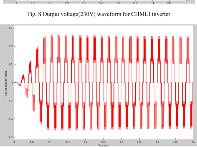
The MATLAB simulation model of CHMLI output voltage and output current waveform is shown in Fig. 8 and Fig. 9
Fig. 8 Output voltage(230V) waveform for CHMLI inverter
Fig. 9 Output current waveform for CHMLI inverter
IV. CONCLUSION
REFERENCES
[1] E. Jimenez-Toribio, A. A. Labour-Castro and F.M.RoDriguez, “SensorlessControll of SEPIC and Cuk Converters for DC Motors using
Solaranels” in proceeding on Electrical Machines and Drives conference, IEMDC-09, 2009, pp 1503-1510.
[2] R. B. Darla, “Development of Maximum Power Point Tracker for PV Panels Using SEPIC Converter” in proceeding on Telecommunications Energy conference, INTELEC 2007, pp 650 655.
[3] B. Santhosh Kumar, S. Arul Daniel, and H. HabeebullahSait, “Analog controller for Photovoltaic array fed inverter driven Single-phase induction motoraq” , in proceeding on Electrical and Electronics Engineering international conference(ELECO2009), pp: I-302-I-305, 2011.
[4] B.Ismail, S.Taib, A. R MohdSaad, M. Isa, C. M. Hadzer, “Development of a Single Phase SPWM Microcontroller-Based Inverter”, in
proceedings on IEEE International Conference of Power and Energy, (PECON-06), pp 437-440.
[5] S. M. Mohaiminul Islam, Gazi Mohammad Sharif, “Microcontroller Based Sinusoidal PWM Inverter for Photovoltaic Application”, in proceedings on first International Conference of Development in Renewable Energy Technology (ICDRET-2010), p-1.
[6] J.G. Llorente,E.I.Oritz-Rivera, A.S. Llinas, “ Analysing the Optimal Matching of DC Motors to Photovoltaic Modules via DC-DC Converters” in proceedings on Applied Power Electronics conference (APEC) ,pp-1062-1068
[7] M.Veerachary and K. S. Shinoy, “ V2- Based Power Tracking for Nonlinear PV Sources” , IEE proceeding on Electrical Power Applications, Vol. 152, No. 5, pp 1263-1270, September 2005.
[8] M.S. Jamri and T.C.Wei, “Modeling and Control of a Photovoltaic Energy System using the State Space Average Technique” in proceeding on American Journal of Applied Science-7, 2010, pp 682-691.