2564 |
P a g e
K.Srineetha
1, C.Madhavi
21
Pursuing M.Tech (DSCE) from Sri Visvesvaraya Institute Of Technology & Science, Chowderpally,
Devarkadra, Mahabubnagar
2
Working as Assistant professor (ECE) from Sri Visvesvaraya Institute Of Technology & Science,
Chowderpally, Devarkadra, Mahabubnagar
ABSTRACT
This paper introduces an on-line transparent test procedure for identifcation of hidden tough errors which im-prove in firstinput firstouptput buffers of routers through field process of NoC. The method engages replicating tests occasionally to avoid storage of errors. A prototype deign of the recommended test algorithm has been combined into the router-channel barrier and on-line test has been achieved with artificial self-parallel data traffic. The presentation of the NoC following summation of the test circuit has been inspected in requisites of throughput whereas the region transparency has been considered by synthesizing the test hardware. Moreover, an on-line test method for the steering logic has been advised which considers utilizing the title darts of the data transfer progress in carrying the test patterns.
Keywords- FIFO buffers, in-field test, NoC, transparent test.
I.
INTRODUCTION
Over the last decade, network-on-chip (NoC) has appeared as a better communication infrastructure compared
with bus-based communication network for complex chip designs avoiding the difficulties related to bandwidth,
signal integrity, and power dissipation. On the other hand, like all additional systems-on-a-chip (SoCs),
NoC-based SoCs must too be tested for faults. Testing the constituents of the NoC infrastructure engages testing
rou-ters and interrouter connections.
Major quantity of region of the NoC information transfer medium is engaged by routers, which is largely
occu-pied by FIFO buffers and routing logic. Consequently, the possibilities of run-time mistakes or errors happening
in buffers and logic are significantly greater compared with the other components of the NoC. Thus, test method
for the NoC transportation must start with test of buffers and routing logic of the routers. Moreover, the test
must be presented sporadically to guarantee that no error gets collected.
The sporadic run-time practical mistakes have been solitary of the main apprehensions through testing of
ex-tremely balanced CMOS-supported memories. These mistakes are a artifact of substantial consequences, like as
ecological weakness, timing, and less supply voltage and thus are intermittent (nonpermanent indicating device damage or malfunction) in nature. However, these intermittent mistakes regularly reveal a comparatively great incidence rate and finally be likely to turn into permanent. Furthermore, exhaust of memories too origin
2565 |
P a g e
test method that would identify the run-time mistakes, which are broken in environment but regularly turn into
stable eventually.
A. Contribution
In this thesis, we have projected an online apparent test procedure for first-input first-output (FIFO) buffers and
steering logic there inside the routers of the NoC transportation. Our involvements are as trails. An apparent
SOA-MATS++ test generation algorithm has proposed targeting in-field eternal mistakes enhanced in
SRAM-based FIFO memories and it has been developed to operate online and sporadic test of FIFO memory there
in-side the routers of the NoC. Moreover, we have too projected an online test method for the steering logic that is
achieved concurrently with the analysis of buffers. The proposal contributes two approaches of consuming the
unexploited portion of the title darts of the incoming data packets in transporting the test patterns. First,
deter-ministic test models for the routing logic produced by Tetramax are situated in the unexploited fields of the title dart and are moved through the common cycle. Subsequent, the pseudorandom models in the artificial data
traf-fic utilized through usual process and incoming at the steering logic are considered as test patterns. Fault
cover-age is calculated for each of the two proposals.
B. Fault Models Considered for the Work
The run-time permanent faults considered in this brief are assumedto be intermittent mistakes, which have turn into eternal eventually. Accordingly, the fault models believed in this thesis are that of intermittent mistakes.
The main factors that direct to intermitent mistakes are timing results, for instance time-dependent dielectric
breakdown (TDDB), electromigration, negative bias temperature instability (NBTI), and hot carrier injection
(HCI). TDDB is a event wherever the oxide below the gatematerial of an MOSFET humiliates over time
result-ing in a short circuit, which are sculpted as stuck-at-faults. Electromigrationdecreases interrelate conductivity
with way of time and directs toopen circuit. The open circuits sourced by electromigration areformed as
stuck-open-faults. NBTI and HCI boost the threshold voltage of transistors directing to reduce in mobility.
Conse-quently,the performances of the memory core reduces bringing in read andwrite failures. The write failures are
sculpted as transition errors,while read failures are sculpted as read disturb faults.
To review, the objective fault models believed for this thesis are stuck-at fault, stuck-open fault, read disturb
fault, and transition fault. Exhaustive performance of these faults can be found.
As error tolerance in NoC scheme has increased consequence among investigate society, many of
ar-ticles have been distributed enveloping unusual features of fault tolerance, such as failure methods, fault
model-ing, analysis, and so on. A complete review precising the research work in these papers has been produced.
Above the years, researchers have suggested many of Design- For-Testability (DFT) systems for NoC
transpor-tation testing (testing routers as well as NoC interconnect) and for NoC based core testing. Built-in self test
2566 |
P a g e
and router checking produces a review of the DFT procedures occupied for testing NoC interconnects and
rou-ters in meticulous. Additionally to novel test designs, fault tolerant routing algorithms have too been proposed.
FIFO buffers in NoC transportation are huge in amount and extend all over the chip. Consequently, possibility
of errors is majorly upper for the buffers evaluated with other components of the router. Together online and
offline test procedures have been projected for test of FIFO buffers in NoC. The scheme is an offline test
proce-dure (appropriate for the identification of creating error in FIFO buffers) that recommends an allocated BIST
controller for FIFO buffers. Online test procedures for the identification of errors in FIFO buffers of NoC
rou-ters have been projected. On the other hand, the procedure believes standard cell-based FIFO buffers, as we
be-lieve SRAM-based FIFO architectures. As a result, errors considered in this thesis are unusual from those
tar-geted.
To the excellent of our data, no occupation has been accounted in the survey that suggests online test of
SRAM-based FIFO buffers there inside routers of NoC transportation. As a result, we inspected online test procedures
for SRAM-based FIFOs in common. The analysis exposed that SRAM based FIFOs are checked exploiting
ei-ther of the trailing two ways, contributed BIST move toward as projected and or allocated BIST proposed.
However, together contributed and allocated BIST move towards being offline test procedures not pass to
iden-tify permanent errors, which enhance eventually.
III. PROPOSED TRANSPARENT TEST GENERATION
The errors believed in this thesis, if exploited for SRAMs or DRAMs, can be identified employing standard
March tests. On the other hand, if the similar set of errors are believed for SRAM-type FIFOs, March test would
not be used openly because of the address limitation in SRAM-type FIFOs and as a result we were encouraged
to prefer single-order address MATS++ test (SOA-MATS++) for the recognition of mistakes believed in this
thesis. The wordoriented SOA-MATS++ test is characterized as {_ (wa); ↑ (ra,wb); ↓ (rb,wa)}; _ (ra)} where, a
is the data background and b is the inversion of the data background. ↑ and ↓ are increasing and decreasing ad-dressing order of memory, respectively. ↕ means memory adad-dressing can be increasing or decreasing.
Applica-tion of SOA-MATS++ test to the FIFO occupies writing patterns into the FIFO memory and reading them back.
Consequently, the memory indexes are destroyed. However, online memory test techniques involve the
restitu-tion of the memory indexes after test. As a result, researchers have changed the March tests to apparent March
test so that tests can be operated without the requirement of external data background and the memory indexes
can be renovated after test. We have accordingly converted the SOA-MATS++ test to apparent SOA-MATS++
(TSOA-MATS++) test that can be applied for online test of FIFO buffers. The apparent SOA-MATS++ test
produced is characterized as {↑ (rx,w¯x, r ¯x,wx, rx)}.
2567 |
P a g e
The algorithmic explanation of the apparent SOA-MATS++ test is illustrated in Algorithm 1. It explains the step
by-step procedure to operate the three stages of the apparent SOA-MATS++ test for every position of the FIFO
memory. The objective position for test is specified by the loop index i to facilitate fluctuates from 0 to N − 1,
where N is the apparent SOA-MATS++ Test Algorithm amount of positions in the FIFO memory. In other terms, i denotes the address of the FIFO memory location currently under test. For every position, the three test runs are presented through three stages of the loop index j.
Algorithm 1. Transparent SOA-MATS++ Test Algorithm
For a meticulous FIFO memory position (present value of
i
), the primary stage of
j
(address run1)
functions the invert phase, where the content of the FIFO position is reversed. The invert test phase
occupies reading the content of
lut
keen on a transitory variable
temp
and then supporting it up in
original
. Then, the complemented content of
temp
is written back to
lut
. At this moment, the content
of
lut
is complement of content of
original
.
In the subsequently stage of
j
(address run2), the reinstate phase is operated. The content of
lut
is
reread into
temp
and evaluated with the content of
original
. The evaluation can outcome in all 1’s
pat-tern. However, deviation from the all 1’s pattern at any bit position represents fault at that meticulous
bit position. Subsequently, the complemented content of
temp
is written back to
lut
. As a result, the
content of
lut
, which were inverted after the primary stage get restored after the second.
The third stage of
j
operates only a read function of
lut
, wherever the content of
lut
is read into
temp
and evaluated with the contents of
original
. At this stage of the test, all 0’s pattern in the result
indi-cates fault free location, while deviation at any bit position from all 0’s patern means fault at that
un-2568 |
P a g e
detected during the previous two test runs. At the finish of the three test runs (iterations of
j
), the loop
index
i
is incremented by one to mark the begin of test for the next location.
B. Fault Coverage of the Proposed Algorithm
For test of stuck-at fault, transition fault, and read disturb fault fault tests enhanced through field function of
FIFO memories is the apparent SOA-MATS++ algorithm. The error exposure of the algorithm is illustrated in
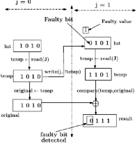
Fig. 1. In mutually the figures, the word size of FIFO memory is supposed to be of 4 bits. The text in italics
against the arrows denotes the operation functioned, while the text in bold font communicates to the variables
used in Algorithm 1.
As illustrated in Fig. 1, assume the data word present in lut be 1010. The test cycles start with the reverse stage (memory address pointer j with 0 value) through which the content of location addressed is read into temp and then backed up in the original. The data written back to lut is the complement of content of temp. Thus, by the finish of the cycle, the data perform in temp and original is 1010, while lut includes 0101. Let a stuck-at-1 error at the most significant bit (MSB) position of the term accumulated in lut. Therefore, in place of accumulating 0101, it essentially accumulates 1101 and accordingly, the stuck-at-error at the MSB obtains motivated.
Fig. 1. Fault detection during invert phase and restore phase
of the transparent SOA-MATS++ test
During the next stage of
j
, when
lut
is readdressed, the data read into
temp
is 1101. At this moment,
the data perform in
temp
and
original
are compared (bitwise XORed). An all 1’s pattern is projected
as result. Any 0 within the pattern would mean a stuck-at fault at that bit position. This situation is
2569 |
P a g e
for a bit location is unusual from the faulty bit value, the stuck-at-fault cannot be detected for the bit
position after the reinstate phase of the test. It needs another test cycle to excite such faults.
IV. IMPLEMENTATION OF THE TEST ON FIFO BUFFERS OF NOC ROUTERS
In this section, we present the method used for performing the projected apparent SOA-MATS++ test on a mesh-type NoC.
Data packets are separated into flow control units (flits) and are sent in pipeline fashion. The dart progress in a mesh-type
NoC infrastructure believed for this work is assumed to require buffering only at the input channels of routers. Thus, for a
data traffic progress from single core to different, the online test is operated only on the eexcite channel FIFO buffers, which
recline beside the path. The buffers perform in two modes, the normal mode and the test mode. The normal mode and test
mode of operation of a FIFO buffer are coordinated with two different clocks. The clock used for test intention (referred as
test_clk in this thesis) is an earlier clock evaluated with the clock required for normal mode (router clock).
The FIFO buffers are allowed to be effective in normal mode for adequate quantity of time before starting their test
proce-dure. This delay in test start produces adequate time for run-time intermittent faults enhaned in FIFO buffers to convert into
eternal faults. The test procedure of a objected FIFO buffer is started by a counter, which controles the FIFO buffer from
normal mode to test mode. The switching of FIFO buffers from normal mode to test mode happens following a definite
pe-riod of time without caring about the present state of the FIFO buffer. It can be disputed that at the instant of switching, the
buffer may not be full, and accordingly not all locations would be ensured through the test cycle. However, test beginning
after the buffer obtains full can cause the following problems. First, wait for the buffer to get complete would unreasonably
delay the test initiation process and would allow faults to get accumulated. Second, test of the complete buffer can extend the
test time and can negatively affect the normal mode of operation.
A test burst occupies series of test read and write cycles. It needs three read and two write cycles, or in other terms three
cycles of the faster test clock to operate an apparent SOA-MATS++ test on a distinct position of a FIFO buffer. It can be
disputed that through a test burst, not all FIFO buffer locations are tested or a test of a location can get interrupted. These
two problems can be avoided by periodically testing the FIFO buffers. Sporadic testing of a FIFO buffer permits test of a
different set of positions of the FIFO buffer in each test burst. Each time the buffer is switched to test mode, the normal
process gets interrupted. The FIFO memory position currently addressed in regular mode, at the instant of switching,
be-comes the objective position for test. Because regular function is suspended at different instants in different test bursts, the
locations tested in each burst would be different. As a result, recuring the test bursts for a numeral times on a FIFO buffer
would cover the test of each location as the figure of positions in a FIFO buffer is few. Moreover, periodic testing avoids
accumulation of error in the buffer.
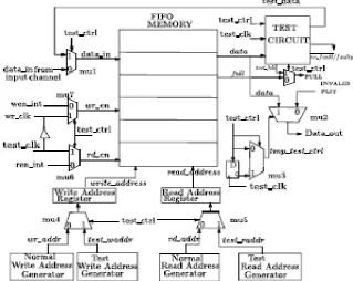
A. Test Architecture
The FIFO buffer perform in every input channel of an NoC router contains of a SRAM-based FIFO memory of
certain depth. Through common function, data darts enter into a data_in line of the buffer and are then accumu-lated in unusual positions of the FIFO memory. On appeal by the neighboring router, the data darts accumuaccumu-lated
are exceeded on to the response port through the data_out line. Fig. 2(a) repesents the FIFO memory with da-ta_in and data_out line. To perform the apparent SOA-MATS++ test on the FIFO buffer, we inserted a test cir-cuit, few multiplexers and logic gates to the surviving hardware, as illustrated in Fig. 2(a). The read and write
functions on the FIFO buffer are controlled by the read enable and write enable lines, correspondingly. The
2570 |
P a g e
procedure, the write enable and read enable are coordinated with the test clock. As mentioned previous, the read
and write functions during test are operated at alternate edges of a test clock. The read functions are coordinated
with the positive edges, whereas the write_clk is achieved by inverting the test clock. In test mode (test_ctrl
high), the test read and write addresses are produced by test address generators employed utilizing gray code
counters related to the normal address generation. Multiplexers m4 and m5 are exploited to select between nor-mal addresses and test addresses.
Fig. 2. (a) Hardware implementation of the test process for the FIFO buffers
Fig. 2. (b) Implementation of test circuit
Believe the condition while the FIFO buffer is in normal mode with darts being transferred from the
2571 |
P a g e
to the buffer, or in other terms, the buffer is bolted for the test time. Accordingly, the excite data line
for the FIFO memory is changed from the external
data_in
line to
test_data
line presented from the
test trail. At the changing moment, the dart which was in the procedure of being moved to the
da-ta_out
line is concurrently read into the
Test Circuit
. However, a single clock cycle delay is produced
for the dart to shift to the
data_out
line. This delay guarantees that the dart is not vanished through the
changing moment and is accurately received by the router, which requests for it. The distinct cycle
delay in the trail of the moving dart is assembled by the D-type flip-flop and the multiplexer
m
3, as
illustrated in Fig. 2(a). The dart, which is read in the test trail, is accumulated in a temporary register
temp
and the test procedure begins with this flit.
To avoid packet failure through testing, the
FULL
signal of the FIFO is asserted
high
so that
neigh-boring routers can be avoided from transferring packets to the corresponding router. However,
per-taining such procedure increases the network latency as reflected in the results.
V. SYNTHESIS AND SIMULATION RESULTS
The projected FIFO buffers is designed with the XILINX ISE 14.5 simulation tool and implemented
with Verilog HDL. The RTL diagram and simulation outcomes are displayed below.
2572 |
P a g e
Fig: Internal architectures of RTL diagram
Fig: Synthesis report
2573 |
P a g e
VI. CONCLUSION
In this thesis, we have proposed transparent SOA-MATS++test generation algorithm that would
iden-tify run-time eternal errors grown in SRAM-supported FIFO memories. The projected apparent test is
consumed to achieve online and periodic test of FIFO memory present inside the routers of the NoC.
Sporadic testing of buffers removes gathering of errors and also tolerates test of every position of the
buffer. Simulation results illustrate that sporadic testing of FIFO buffers do not have greatly impact on
the general throughput of the NoC excluding when buffers are tested also frequently. We have too
projected an online test procedure for the routing logic that is achieved concurrently with the test of
buffers and involves utilization of the unexploited fields of the description darts of the received data
packets. Test algorithm and RAM was designed by the Verilog HDL synthesized in Xilinx ISE14.5.
VII. FUTURE SCOPE
We have too projected an online test procedure for the routing logic that is achieved concurrently with
the test of buffers and involves utilization of the unexploited fields of the description darts of the
re-ceived data packets. As prospect effort, we would like to change the projected FIFO testing procedure
that will tolerate received data packets to the router under test without interrupting the test.
REFERENCES
[1] W. J. Dally and B. Towles, “Route packets, not wires: On-chip interconnection networks,” in Proc. 38th Annu. Design Autom. Conf., 2001, pp. 684–689.
[2] A. Bondavalli, S. Chiaradonna, F. Di Giandomenico, and F. Grandoni, “Threshold-based mechanisms to
discriminate transient from intermittent faults,” IEEE Trans. Comput., vol. 49, no. 3, pp. 230–245, Mar. 2000.
[3] M. Radetzki, C. Feng, X. Zhao, and A. Jantsch, “Methods for fault tolerance in networks-on-chip,” ACM Comput. Surv., vol. 46, no. 1, pp. 1–38, Jul. 2013, Art. ID 8.
[4] S. Ghosh and K. Roy, “Parameter variation tolerance and error resiliency: New design paradigm for the na-noscale era,” Proc. IEEE, vol. 98, no. 10, pp. 1718–1751, Oct. 2010.
[5] S. Borri, M. Hage-Hassan, L. Dilillo, P. Girard, S. Pravossoudovitch, and A. Virazel, “Analysis of dynamic
faults in embedded-SRAMs: Implications for memory test,” J. Electron. Test., vol. 21, no. 2, pp. 169–179, Apr. 2005.
[6] M. Bushnell and V. Agrawal, Essentials of Electronic Testing for Digital, Memory and Mixed-Signal VLSI Circuits (Frontiers in ElectronicTesting). New York, NY, USA: Springer-Verlag, 2000.
[7] D. Xiang and Y. Zhang, “Cost-effective power-aware core testing in NoCs based on a new unicast-based multicast scheme,” IEEETrans. Comput.-Aided Design Integr. Circuits Syst., vol. 30, no. 1, pp. 135–147, Jan. 2011.
2574 |
P a g e
[9] D. Xiang, “A cost-effective scheme for network-on-chip router and interconnect testing,” in Proc. 22nd Asian Test Symp. (ATS), Nov. 2013, pp. 207–212.
[10] M. Ebrahimi, M. Daneshtalab, J. Plosila, and H. Tenhunen, “Minimal-path fault-tolerant approach using
connection-retaining structure in networks-on-chip,” in Proc. 7th IEEE/ACM Int. Symp. Netw. Chip (NoCS), Apr. 2013, pp. 1–8.