1421 |
P a g e
Efficient 500 MHz Digital Phase Locked Loop
Implementation sin 180nm CMOS Technology
Akash Singh Rawat
1, Kirti Gupta
2Electronics and Communication Department, Bharati Vidyapeeth’s College of Engineering, New Delhi
ABSTRACT
In this paper, two versions of Digital Phase Locked Loops(D PLL) have been implemented using the two efficient
Phase frequency detector circuits are presented and their performance is compared through simulation in LTspice
using 180nm CMOS technology parameters. A Phase frequency detector (PFD) is a key component of DPLL and
governs the locking range and locking time of DPLL. PFDcircuits used in DPLL implementation are more sensitive
than traditional PFDas there arefree from the problem of dead zone.
Keywords: Digital, FPGA, PLL
I INTRODUCTION
Digital Phase locked loop (DPLL) is avital component of almost all the modern electronics as well as
communication systems [1-3]. They are employed as frequency synthesizer at high frequency in wide variety of
applications that includes microprocessors, FPGA, well timed clocks and recovery of signal from noisy
communication channel for modern wireless communication devices.The basic purpose of a DPLLs is to generate
well-timed on-chip clocks in high-speed digital systems as the crystals oscillators are unable to generate the high
frequency clock due to the mechanical limitations imposed on them. The incorporation ofDPLL in a single chip,
makes it an essential component in modern wireless devices which are compact, portable and battery operated with
decreased risk of reliability problems. Hence, modern wireless communication systems employ DPLL mainly for
synchronization, clock synthesis, skew and jitter reduction [4].
The concept of phase locking was introduced in 1930s and was then adopted in design of efficient communication
systems.It is a closed-loop feedback system that sets fixed phase relationship between its output clock phase and the
phase of a reference clock. PLL is capable of tracking the phase changes that falls in the bandwidth of the PLL.
While the basic phase locked loop remained nearly the same since then, its implementation in different technologies
and for different applications continues to remain as a challenge to the designers. The main objective of a PLL is to
generate a signal in which the phase is the same as the phase of a reference signal. This is achieved after many
1422 |
P a g e
The paper first describes the architecture and the operation of phase locked loop in section 1. In the next section, thetopologies of various PFD circuits [5] available in the literature are described. In the subsequent sections, brief
introduction to TRI-STATE [6], LPF and Current Starved VCO [7] is given. In the section 5, simulation results of
two different implementations of PLL are shown and their performance is compared in terms of lock time,
acquisition range and jitter. Finally, the conclusions are drawn in the last section.
II PHASE LOCKED
LOOP
The basic block diagram of the PLL is shown in the Fig. 1. In general, a PLL consists of five main blocks:
1) Phase Frequency Detector(PFD)
2) Tristate circuit
3) Low Pass Filter (LPF)
4) Voltage Controlled Oscillator (VCO)
5) Divide by N Counter.
Fig. 1 Block diagram of PLL
The Phase frequency Detector (PFD) is one of the main components in PLL circuits. It compares the phase and
frequency difference between the reference clock and the feedback clock. Depending upon the phase and frequency
deviation, it generates two output signals “up” and “down”. The Tri-state circuit is used in the PLL to combine both
the outputs of the PFD and give a single output. The output of the Tri-state circuit is fed to a Low Pass Filter (LPF)
to generate a DC control voltage. The phase and frequency of the “Voltage ControlledOscillator” (VCO) output
depends on the generated DC control voltage. If the PFD generates an “up” signal, the error voltage at the output of
LPF increases which in turn increase the VCO output signal frequency. On the contrary, if a “down” signal is
generated, the VCO output signal frequency decreases. The output of the VCO is then fed back to the PFD in order
to recalculate the phase difference, and this process is repeated until the phase and frequency of the reference clock
1423 |
P a g e
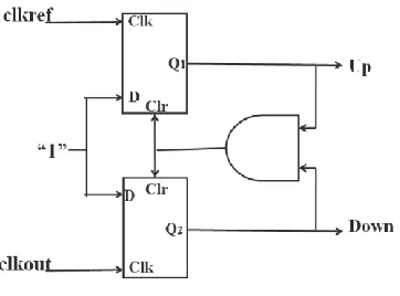
III EFFICIENT PFD
3.1
Traditional PFD
The design consists of two D flip-flops and AND gate to provide a reset path when both outputs go high at the same
time as shown in Fig.2. Due to the reset path this design suffers from large dead zone as some delay is introduced
by the AND gate to reset the D flip flops.
Fig. 2 Traditional PFD
The operation of this circuit is based on two D-type flip-flop and simple AND gate. Each flip-flop has the D-input
wired high. Under this condition, the flip-flop with a low Q output will transition to high on the next rising edge of
its clock input. Also if such a transition occurs when Q is high, then there will no change in the flip-flop state. A
high signal on a reset input will force Q low as soon as the reset signal is applied. Finally, a logically high on both
Q1 and Q2 output causes the resetting of both the flip-flops [4].
The PFD generates two outputs that are not complementary. The output signal depends not only on the phase error,
but also on the frequency error. If the frequency, “clkref” , is less than the “clkout”, then the PFD produces positive
pulses at Q1, while Q2 remains zero. Conversely, if “clkref” > “clkout”, then positive pulses appear at Q2 while Q1=0. If “clkref” = “clkout”, then circuit generates pulses at either Q1 or Q2 with a width equal to the phase
difference between the two inputs. Thus the average value of the Q1 – Q2 is proportional to the frequency or the
phase difference between the inputs at clkref and clkout. The outputs Q1 and Q2 are usually called the “up” and
“down” signals. The “up” pulse is the difference between the phases of the two clock signals. This “up” pulse
indicates that the feedback signal needs to speed up with the reference signal. In the second case, when the feedback
signal is leading the reference clock signal, the “down” pulse represents the difference between the phases of the two
1424 |
P a g e
3.2
Modified PFDs
In this type of PFDs [5] the reset path is modified. The inputs signals “clkref” and “clkout” are directly connected to
the reset signal of another flip flops as shown in the Fig. 3. This modification has enabled us to remove the reset
path and reduce the delay time that causing the dead zone problem in traditional PFD.
Fig. 3 Modified PFD
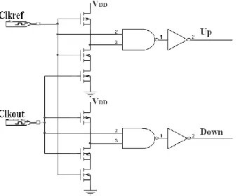
3.2.1 1st Modified PFD
As shown in Fig. 4 the flip-flop schematic design has few changes from thetraditional PFD, this changes allowed
getting rid of the reset path and applying the Clkrefand Clkout signal immediately to the RST input for each flip-flop
to reset them as soon as both flip-flops have high output at the same time. The modified D flip-flop in Fig. 4
operates exactly like traditional PDF. When the Clkref input signal is leading the Up output signal results high and
when Clkout signal is leading it will result Down signal high. The 1st modified PFD shows the dead zone of just 40
ps , which makes it a better candidate for high speed PLL than the traditional PFD, beside the lower power
consumption make this more suitable for PLL implementation in wireless devices that use a limited power
supply.[5]
3.2.2 2nd Modified PFD
To achieve a higher speed PFD than the 1st modified PFD, another design shown in Fig. 5 which eliminates the reset
path and lead to a smaller time delay then 1st modified PFD. To be able to detect the phase error and has a fast reset,
this design depends on detecting the rising and falling edge of the input signals to do the job. Fig. 5 shows the
schematic design of the 2nd modified PFD As we can see instead of having feedback reset path, both “Clkref” and
1425 |
P a g e
Fig. 4 Schematic Diagram of 1
stModified PFD
The 2nd modified PFD shows the dead zone of just 15ps, which is almost zero dead zone and makes it a better
candidate for high speed PLL than the 1st modified PFD also, beside the lower power consumption make this more
suitable for PLL implementation in wireless devices that use a limited power supply. [5]
Fig. 5 Schematic Diagram of 2
ndModified PFD
IV TRI-STATE CIRCUIT AND LOW PASS FILTER
Tri-state circuit [6] is an important block of the whole PLL system. It converts the phase or frequency difference
information into a voltage, used to tune the VCO. Tri-state circuit is used to combine both the outputs of the PFD
and give a single output which is fed to the input of the filter. When both signals, Up and Down, are low, both
MOSFETs are off and the output is in a high-impedance state. If the Up signal goes high, M1 turns on and pulls the
output up to VDD while if the Down signal is high the output is pulled low through M2. The schematic diagram of
1426 |
P a g e
Fig.6Tri-state Circuit
Fig. 7 Loop Filter For Tri-state
The passive low pass loop filter is used with tri-state is shown in Fig. 7. The filter should be as compact as
possible.The output voltage of the loop filter controls the oscillation frequency of the VCO. The loop filter voltage
will increase if Clkref rising edge leads Clkout rising edge and will decrease if Clkout rising edge leads Clkref rising
edge. The LPF behaves as the potential divider for the high frequency variation and integrator for the low frequency
variation.[3] If the PLL is in locked state it maintains a constant value.
VII VOLTAGE CONTROLLED OSCILLATOR
An oscillator is an autonomous system which generates a periodic output depending on the control voltage. The
starved voltage controlled oscillator (CSVCO). We used the 9 stages CSVCO with centre frequency of 500Mhz at
0.9 V. Transistors M4 and M5 operate as an inverter while M3 and M6 operate as current sources. The current
sources, M3 and M6, limit the current available to the inverter, M4 and M5; in other words, the inverter is starved
for current. The desired center frequency can be achieved by the allowing the appropriate current ID to follow in the
inverter with a supply of 1.8V. The CSVCO is designed both in usual manner as mentioned in [7].
Fig. 8 Current Starved V.C.O used in PLL implementations [7]
Characteristic curve of Designed V.C.O is shown in Figure 4.2 in which we have the output frequency of 500MHz
1427 |
P a g e
Fig.9Characteristic Curve of Designed V.C.O
VIII SIMULATION RESULTS
In this section, the proposed PLL architecture by employing the two architectures of the phase detector (Type I, II)
are simulated in LTSPICE using 180 nm CMOS technology parameters. The simulation waveforms corresponding
to VCO output, Eye diagram and clocks in the locked state are shown in Fig. Their performance is measured interm
of locking time, Jitter, VCO fluctuation. The simulation results are listed in Table I. It is observed tha the PLL using
2nd modified phase detector output outperforms Type II PLL in terms of the discussed parameters.
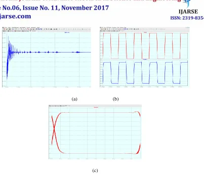
(a) (b)
(c)
Fig. 10Type I PLL a) V.C.O WAVE FORM b) Clkref and Clkout in locked state c) Eye Diagram in
1428 |
P a g e
(a) (b)
(c)
Fig. 11Type II PLL a) V.C.O WAVE FORM b) Clkref and Clkout in locked state c) Eye Diagram
in locked state
Table I : Performance comparison of the two PLLs
Parameters PLL (Type I) PLL (Type
II)
Lock time @500 MHz 1.97us 1.27us
MAXIMUM FREQUENCY LOCKED 819.67MHz 769.23MHz
MINIMUM FREQUENCY LOCKED 108.67MHz 100MHz
ACQUISITION RANGE 711MHz 669.23MHz
VCOin FLUCTUATION IN LOCKED STATE 3.1mV 1.9mV
Jitter @ 0.9V 39.06ps 6.13ps
IX CONCLUSIONS
In the work, two types of PLL operating at the center frequency of 500MHz has been implemented and compared.
1429 |
P a g e
The versions of the PFD do not show the presence of the dead zone in contrast to the traditional PFD. Theperformance of PLL using these two PFDs has been compared in terms of lock time, acquisition range and
fluctuation in VCOin in locked state. Through simulation in LTspice in 180nm, it is found that Type II PLL is better
than Type I in terms of the speed of locking and stability of the locked state.
REFERENCES
[1] R.E. Best, “Phase Locked Loops Design, Simulation and Applications,” McGraw-Hill Publication, 5th Edition,
2003.
[2] Dan H. Wolaver, “Phase Locked Loop Circuit Design,” Prentice Hall Publication, 1991.
[3] R.J.Baker, H.W.Li, and D.E.Boyce, “CMOS Circuit Design, Layout, and Simulation,” IEEE Press Series on
Microelectronic Systems, 2002.
[4] B. Razavi, “Design of Analog CMOS Integrated Circuits,” Tata McGraw Hill Edition,2002.
[5] Mhd Zaher Al Sabbagh, B.S.: 0.18μm Phase Frequency Detector and Charge Pump Design for Digital Video
Broadcasting for Handheld’s Phase-Locked-Loop Systems. Thesis,2007.
[6] Won-Hyo Lee, Sung-Dae Lee, and Jun-Dong Cho. "A High-Speed, Low-Power Phase Frequecy Detector and
Charge_Pump Circuits for HighFrequency Phase-Locked Loops." IEICE Trans. Fundamentals, E82 (1999),
2514- 2520.

![Fig. 8 Current Starved V.C.O used in PLL implementations [7]](https://thumb-us.123doks.com/thumbv2/123dok_us/7782369.1286041/6.612.186.434.483.639/fig-current-starved-v-c-used-pll-implementations.webp)