Summary
Shift registers longer than eight bits can be implemented most efficiently in XC4000E Select-RAMTM. Using Linear Feedback Shift-Register (LFSR) counters to address the RAM makes the design even simpler. This application note describes 4- and 5-bit universal LFSR counters, very efficient RAM-based 32-bit and 100-bit shift registers, and pseudo-random sequence generators with repetition rates of thousands and even trillions of years, useful for testing and encryption purposes. The appropriate taps for maximum-length LFSR counters of up to 168 bits are listed.
Introduction
The XC4000E on-chip distributed synchronous RAM archi-tecture lends itself well to the efficient implementation of long shift registers. The 16 x 1 or 32 x 1 RAM behaves like an edge-triggered register. An address counter supplies sequential addresses, but there is no need for a conven-tional binary address sequence. Any repetitive pattern is acceptable, and a linear feedback shift register counter is the most efficient. In the examples below the conventional LFSR counter algorithm has been modified to guarantee no lock-up, even in the all-ones state.
Note that the established literature describes the outputs of LFSRs as Q1 to Qn (not Q0 to Qn-1, as is customary in binary counters). In order to be consistent with prior litera-ture, LFSR bits are therefore labeled 1 to n throughout this application note.
LFSR Counters
For a 4-bit counter, the basic XNOR feedback from Q3 and Q4 would exclude the all-ones state. By decoding the two states where the lower three bits are all ones, and inverting
the feedback for those states, the 4-bit LFSR counter counts modulo 16, and has no lock-up state. Counters with a shorter cycle require additional decoding of the feedback signal, as shown inTable 1 andFigure 1. Any such decod-ing is easily done in the front-end CLB function generator. For a 5-bit counter,Table 2 shows the connections required for dividing by any number up to 32.
Efficient Shift Registers, LFSR
Counters, and Long
Pseudo-Random Sequence Generators
XAPP 052 July 7,1996 (Version 1.1) Application Note by Peter Alfke
Xilinx Family
XC4000E, XC4000L, XC4000EX, XC4000XL
Demonstrates
Shift registers implemented in RAM LFSR counters
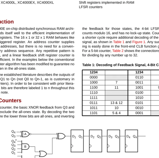
Table 1: Decoding of Feedback Signal, 4-Bit Counter
1234 1234 0000 0110 3 1000 7 0011 11 1100 11 1001 9 & 8 1110 0100 14 1111 1010 6 0111 13 & 12 0101 2 1011 10 0010 5 1101 5 & 4 0001
Figure 1: Divide by 5 to 16 Counter
D4 Q4 D3 Q3 D2 Q2 D1 Q1 Q4 Q3 Q4 Q3 Q2 Q1 A B C * X5801
APPLICATION NOTE
Efficient Shift Registers, LFSR Counters, and Long Pseudo-Random Sequence Generators
Divide-By 5 to 16 Counter in Two CLBs
Feedback for÷16:
(Q3 XNOR Q4) XOR (Q1 AND Q2 AND Q3)
To divide by a number smaller than 15, use AND gate “C” in Figure 1 to decode the binary pattern listed inTable 1 next to the desired number. For÷15 and any number listed to
the right of the & symbol, also add Q4 to AND gate “B”, thus skipping the all-ones state. All of these counters avoid lock-up in the all-ones state.
• For÷16: do not connect Q4 to AND gate “B”, do not use AND gate “C”
• For÷15: connect Q4 to AND gate “B”, do not use AND gate “C”
• For÷<15: program AND gate “C" according to the table • For÷ 4, 8,12,15: connect Q4 to AND gate “B”
• For all other numbers:
do not connect Q4 to AND gate “B”
Divide-By 2 to 32 Counter in 2.5 CLBs
Feedback for÷32:
(Q3 XNOR Q5) XOR (Q1 AND Q2 AND Q3 AND Q4) To divide by a number smaller than 31, use AND gate “C” in Figure 2 to decode the binary pattern listed inTable 2 next to the desired number. For÷31 and any number listed to the right of the & symbol, also add Q5 to AND gate “B”, thus skipping the all-ones state. All of these counters avoid lock-up in the all-ones state.
• For÷32: do not connect Q5 to AND gate “B”, do not use AND gate “C”
• For÷31: connect Q5 to AND gate “B”, do not use AND gate “C”
• For÷<31: program AND gate “C” according to the table • For÷5,10,14,16,18, 22, 27, 31:
connect Q5 to AND gate “B” • For all other numbers:
do not connect Q5 to AND gate “B”
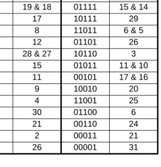
Table 2: Decoding of Feedback Signal, 5-Bit Counter
12345 12345 00000 11101 13 10000 23 & 22 11110 31 11000 7 11111 11100 19 & 18 01111 15 & 14 01110 17 10111 29 00111 8 11011 6 & 5 10011 12 01101 26 01001 28 & 27 10110 3 00100 15 01011 11 & 10 00010 11 00101 17 & 16 10001 9 10010 20 01000 4 11001 25 10100 30 01100 6 01010 21 00110 24 10101 2 00011 21 11010 26 00001 31
Figure 2: Divide by 2 to 32 Counter
D4 Q4 D5 Q5 D3 Q3 D2 Q2 D1 Q1 Q5 Q3 Q5 Q4 Q3 Q2 Q1 A B C * X5802
Product Obsolete/Under Obsolescence
RAM-Based Shift Registers
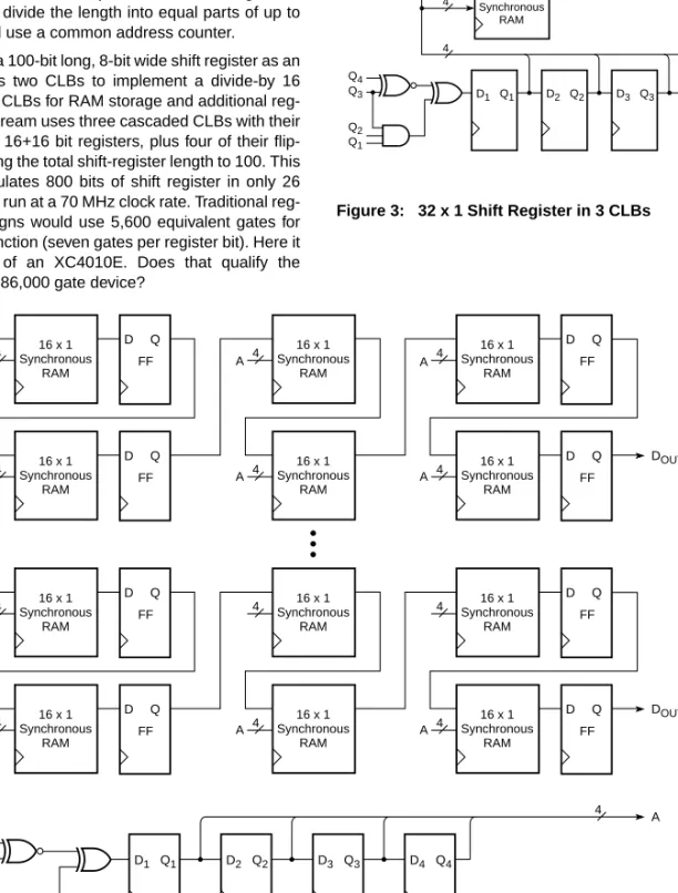
As shown inFigure 3, a 32 x 1 shift register design requires two CLBs for the÷16 address counter plus one CLB for the RAM. An 8-bit wide, 32-bit long shift register would use seven additional CLBs for RAM storage and output regis-ters. Wider and longer shift registers can easily be imple-mented using the same concept. For increased length, it is most efficient to divide the length into equal parts of up to 16 bits each and use a common address counter. Figure 4 shows a 100-bit long, 8-bit wide shift register as an example. It uses two CLBs to implement a divide-by 16 counter, plus 24 CLBs for RAM storage and additional reg-isters. Each bitstream uses three cascaded CLBs with their RAMs acting as 16+16 bit registers, plus four of their flip-flops used to bring the total shift-register length to 100. This design thus emulates 800 bits of shift register in only 26 CLBs, and it can run at a 70 MHz clock rate. Traditional reg-ister-based designs would use 5,600 equivalent gates for this complete function (seven gates per register bit). Here it occupies 6.5% of an XC4010E. Does that qualify the XC4010E as an 86,000 gate device?
Figure 3: 32 x 1 Shift Register in 3 CLBs
D4 Q4 D3 Q3 D2 Q2 D1 Q1 DOUT DOUT DIN DIN Q4 Q3 Q2 Q1 X5803 16 x 1 Synchronous RAM 4 4 4 16 x 1 Synchronous RAM
Figure 4: 100 x 8 Shift Register in 26 CLBs
D4 Q4 D3 Q3 D2 Q2 D1 Q1 DIN (8) DOUT (1) Q4 Q3 Q2 Q1 D Q X5804 4 4 FF A 16 x 1 Synchronous RAM 4 Synchronous16 x 1 RAM D Q 4 FF 16 x 1 Synchronous RAM D Q 4 FF 16 x 1 Synchronous RAM 4 Synchronous16 x 1 RAM D Q 4 A A A FF 16 x 1 Synchronous RAM DIN (8) DOUT (8) D Q 4 FF 16 x 1 Synchronous RAM 4 Synchronous16 x 1 RAM D Q 4 FF 16 x 1 Synchronous RAM D Q 4 FF 16 x 1 Synchronous RAM 4 Synchronous16 x 1 RAM D Q 4 A A A A A A FF 16 x 1 Synchronous RAM
Efficient Shift Registers, LFSR Counters, and Long Pseudo-Random Sequence Generators
Pseudo-Random Sequence
Generator in Four CLBs
Any long LFSR counter generates a long pseudo-random sequence of zeros and ones. The sequence is not exactly random since it repeats eventually, and it also follows a mathematically predictable sequence. But for most practi-cal purposes it can be considered random.
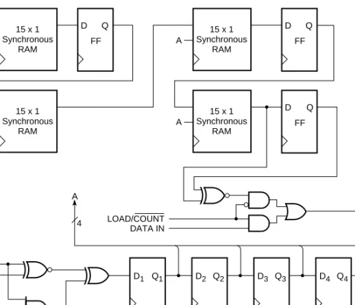
A 63-bit LFSR counter has a repetition time of (263-1) clock periods. Running at 50 MHz, such a counter repeats after more than five thousand years (5,849 years to be more pre-cise), which is long enough to be irrelevant for most practi-cal purposes. Conceptually, a 63-bit LFSR counter consists of a 63-bit shift register, with an XNOR feedback from the last stage and the next-to-last stage. (SeeFigure 5.) The 63-bit length was actually chosen because of its conve-niently simple feedback. Other maximum-length LFSR counters require different XNOR feedback taps. Table 3 describes the maximum-length feedback connections for all LFSR counters of up to 168 bits in length.
The conventional shift register implementation of a 63-bit LFSR counter requires 32 CLBs in XC3000 or XC4000 family devices. By using a RAM-based approach, only two CLBs are needed, plus the addressing counter, which can be a÷15 LFSR counter in two CLBs. With proper partition-ing, the complete 63-bit pseudo-random sequence genera-tor shown in Figure 5 requires only four CLBs, and is capable of running at up to 70 MHz. A starting pattern of up to 63 bits can be first loaded into the shift register, and the output then generates a pseudo-random sequence of zeros and ones. The design can be expanded to a 127-bit LFSR counter in six CLBs, or a 159-bit LFSR counter in seven CLBs. Either of these two counters has a repetition period many billion times longer than the life of the universe.
Figure 5: 63-Bit LFSR Counter in 4 CLBs
D4 Q4 D3 Q3 D2 Q2 D1 Q1 Q4 Q3 Q2 Q1 D Q X5805 4 FF A 15 x 1 Synchronous RAM D Q FF 15 x 1 Synchronous RAM 15 x 1 Synchronous RAM D Q A A A A FF LOAD/COUNT DATA IN 15 x 1 Synchronous RAM
Linear Feedback Shift Register Taps
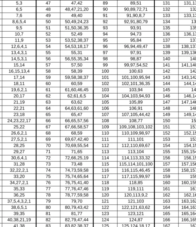
This table lists the appropriate taps for maximum-length LFSR counters of up to 168 bits. The basic description and the table for the first 40 bits was originally published in XCELL and reprinted on page 9-24 of the 1993 and 1994 Xilinx Data Books.Responding to repeated requests, the list is here extended to 168 bits. This information is based on unpublished research done by Wayne Stahnke while he was at Fairchild Semiconductor in 1970.
Table 3: Taps for Maximum-Length LFSR Counters
n XNOR from n XNOR from n XNOR from n XNOR from
3 3,2 45 45,44,42,41 87 87,74 129 129,124 4 4,3 46 46,45,26,25 88 88,87,17,16 130 130,127 5 5,3 47 47,42 89 89,51 131 131,130,84,83 6 6,5 48 48,47,21,20 90 90,89,72,71 132 132,103 7 7,6 49 49,40 91 91,90,8,7 133 133,132,82,81 8 8,6,5,4 50 50,49,24,23 92 92,91,80,79 134 134,77 9 9,5 51 51,50,36,35 93 93,91 135 135,124 10 10,7 52 52,49 94 94,73 136 136,135,11,10 11 11,9 53 53,52,38,37 95 95,84 137 137,116 12 12,6,4,1 54 54,53,18,17 96 96,94,49,47 138 138,137,131,130 13 13,4,3,1 55 55,31 97 97,91 139 139,136,134,131 14 14,5,3,1 56 56,55,35,34 98 98,87 140 140,111 15 15,14 57 57,50 99 99,97,54,52 141 141,140,110,109 16 16,15,13,4 58 58,39 100 100,63 142 142,121 17 17,14 59 59,58,38,37 101 101,100,95,94 143 143,142,123,122 18 18,11 60 60,59 102 102,101,36,35 144 144,143,75,74 19 19,6,2,1 61 61,60,46,45 103 103,94 145 145,93 20 20,17 62 62,61,6,5 104 104,103,94,93 146 146,145,87,86 21 21,19 63 63,62 105 105,89 147 147,146,110,109 22 22,21 64 64,63,61,60 106 106,91 148 148,121 23 23,18 65 65,47 107 107,105,44,42 149 149,148,40,39 24 24,23,22,17 66 66,65,57,56 108 108,77 150 150,97 25 25,22 67 67,66,58,57 109 109,108,103,102 151 151,148 26 26,6,2,1 68 68,59 110 110,109,98,97 152 152,151,87,86 27 27,5,2,1 69 69,67,42,40 111 111,101 153 153,152 28 28,25 70 70,69,55,54 112 112,110,69,67 154 154,152,27,25 29 29,27 71 71,65 113 113,104 155 155,154,124,123 30 30,6,4,1 72 72,66,25,19 114 114,113,33,32 156 156,155,41,40 31 31,28 73 73,48 115 115,114,101,100 157 157,156,131,130 32 32,22,2,1 74 74,73,59,58 116 116,115,46,45 158 158,157,132,131 33 33,20 75 75,74,65,64 117 117,115,99,97 159 159,128 34 34,27,2,1 76 76,75,41,40 118 118,85 160 160,159,142,141 35 35,33 77 77,76,47,46 119 119,111 161 161,143 36 36,25 78 78,77,59,58 120 120,113,9,2 162 162,161,75,74 37 37,5,4,3,2,1 79 79,70 121 121,103 163 163,162,104,103 38 38,6,5,1 80 80,79,43,42 122 122,121,63,62 164 164,163,151,150 39 39,35 81 81,77 123 123,121 165 165,164,135,134 40 40,38,21,19 82 82,79,47,44 124 124,87 166 166,165,128,127 41 41,38 83 83,82,38,37 125 125,124,18,17 167 167,161 42 42,41,20,19 84 84,71 126 126,125,90,89 168 168,166,153,151 43 43,42,38,37 85 85,84,58,57 127 127,126 44 44,43,18,17 86 86,85,74,73 128 128,126,101,99
Efficient Shift Registers, LFSR Counters, and Long Pseudo-Random Sequence Generators
LFSR Counters, 3 to 168 Bits
Conventional binary counters use complex or wide fan-in logic to generate high end carry signals. A much simpler structure sacrifices the binary count sequence, but achieves very high speed with very simple logic, easily packing two bits into every CLB. Such Linear Feedback Shift-Register (LFSR) counters are also known as pseudo-random sequence generators.
An n-bit LFSR counter can have a maximum sequence length of 2n-1. In that case, it goes through all possible code permutations except one, which would be a lock-up state. A maximum length n-bit LFSR counter consists of an n-bit shift register with an XNOR in the feedback path from the last output Qn to the first input D1. The XNOR makes the lock-up state the all-ones state; an XOR would make it the all-zeros state. For normal Xilinx applications, all-ones is more easily avoided, since “by default” the flip-flops wake up in the all-zeros state.Table 3 describes the outputs that must be used as inputs of the XNOR. LFSR outputs are tra-ditionally labeled 1 through n, with 1 being the first stage of the shift register, and n being the last stage. This is different from the conventional 0 to (n-1) notation for binary counters. A multi-input XNOR is also known as an even-parity circuit. Note that the connections described in this table are not necessarily unique; certain other connections may also result in maximum length sequences.
Examples
• A 10-bit shift register counts modulo 1023, if the input D1 is driven by the XNOR of Q10 and the bit three positions to the left (Q7), i.e. a one is shifted into D1 when Q10 and Q7 have even parity, which means they are identical.
• An 8-bit shift register counts modulo 255 if the input D1 is driven by the XNOR of Q8, Q6, Q5, Q4, i.e., a one is shifted into D1 if these four outputs have even parity, (four zeros, or two ones, or four ones).
References:
Wayne Stahnke,Primitive Polynomials Modulo Two, private communication in 1970, giving the following references: E.R. Berlekamp, Algebraic Coding Theory, McGraw-Hill, 1968
P.H.R. Scholefield,Shift Registers Generating Maximum-Length Sequences, Electronic Technology, 10-1960, pp. 389-394
S.W. Golomb, Shift Register Sequences, Holden-Day, San Francisco, 1967
E.J. Watson,Primitive Polynomials (Mod 2), Math. Comp. v.16 pp. 368, 1962
N. Zierler and J. Brillhart, On Primitive Trinomials, Information and Control v. 13, pp 541-554, 1968, and v. 14, pp. 566-569, 1969
R.W. Marsh, Table of Irreducible Polynomials, Dept. of Commerce, October 1957
H. Riesel, En Bok om Primtal, Studentlitteratur, Denmark, 1968
M. Kraitchik,Théorie dés Nombres, Gauthier-Villars, Paris, 1922 and 1952
M. Kraitchik, On the Factorization of 2n ±1, Scripta Mathematica, v. 18, pp. 39-52, 1952
J. Brillhart,Miscellaneous Factorizations, Math. Comp., v. 17 pp. 447-450, 1963
J. Brillhart and J.L.Selfridge, Factorizations..., Math. Comp., v. 21, pp. 87-96, 1967
K.R. Isemonger,Additional Factorizations..., Math. Comp., v. 19, pp. 145-146, 1965
R.M. Robinson,Some Factorizations..., Math. Comp., v. 11, pp. 265-268, 1957
The Programmable Logic Company
SM© 1996 Xilinx, Inc. All rights reserved. The Xilinx name and the Xilinx logo are registered trademarks, all XC-designated products are trademarks, and the Pro-grammable Logic Company is a service mark of Xilinx, Inc. All other trademarks and registered trademarks are the property of their respective owners. Xilinx, Inc. does not assume any liability arising out of the application or use of any product described herein; nor does it convey any license under its patent, copy-right or maskwork copy-rights or any copy-rights of others. Xilinx, Inc. reserves the copy-right to make changes, at any time, in order to improve reliability, function or design and to supply the best product possible. Xilinx, Inc. cannot assume responsibility for the use of any circuitry described other than circuitry entirely embodied in its prod-ucts. Products are manufactured under one or more of the following U.S. Patents: (4,847,612; 5,012,135; 4,967,107; 5,023,606; 4,940,909; 5,028,821; 4,870,302; 4,706,216; 4,758,985; 4,642,487; 4,695,740; 4,713,557; 4,750,155; 4,821,233; 4,746,822; 4,820,937; 4,783,607; 4,855,669; 5,047,710; 5,068,603; 4,855,619; 4,835,418; and 4,902,910. Xilinx, Inc. cannot assume responsibility for any circuits shown nor represent that they are free from patent infringement or of any other third party right. Xilinx, Inc. assumes no obligation to correct any errors contained herein or to advise any user of this text of any correction if such be made.
Headquarters Xilinx, Inc. 2100 Logic Drive San Jose, CA 95124 U.S.A. Tel: 1 (800) 255-7778 or 1 (408) 559-7778 Fax: 1 (800) 559-7114 Net: [email protected] Web: http://www.xilinx.com