STATIC RANDOM ACCESS MEMORY
USING QUATERNARY D LATCH
VASUNDARA PATEL K S1,K S GURUMURTHY2, VINAY SHESHADRI3, SIVARAM KRISHNAN R4
1
Dept of ECE, BMSCE,VTU, 2Dept of E&C, UVCE, Bangalore University 3 NetApp India Pvt Ltd, 4Mistral Solutions Pvt. Ltd,Bangalore, Karnataka, India
Abstract:
In this paper, the implementation of a static random access memory cell using quaternary logic is presented. This static RAM is based on quaternary D latch. When the select line is asserted, the stored data is placed on the cell’s output. When both select and write are asserted the D latch is open and a new data bit is stored. The D latch used here is built using NMAX, NMIN and quaternary inverter circuits. A 4x4 memory array have also been designed and compared with 4x4 array of Quaternary Static CMOS memory Cell.. The spice coding is done using 0.18µm CMOS technology and verification of the design is done through HSPICE and COSMOSSCOPE Synopsis Tools. Power and delay of the circuit is analyzed. New design shows 65.28% of improvement in average power dissipation when compared to 4x4 array of Quaternary Static CMOS memory Cell and 75% improvement over binary 4X4 array at 180nm.
Keywords: Multiple-valued logic, Quaternary logic, CMOS memory integrated circuit, Quaternary D latch.
1. Introduction
The history of Multiple-valued logic (MVL) as a separate subject began in the early 1920 by a polish philosopher Lukasiewicz. His intention was to introduce a third additional value to binary. The outcome of this investigation is known the Lukasiewicz system. Parallel to this approach the American mathematician Emil Post introduced multiple-valued algebra known as post algebra.
In modern SOC design, the interconnection is becoming a major problem because of the bus width. This problem can be solved by using Multiple-valued logic interconnection [1]. For example a conventional 16 - bit bus (0 and 1) represents 65536 combinations. If we code the output with Quaternary logic (0, 1, 2 and 3), the width of the bus is reduced from 16 to 8. As a result, we can reduce power and area requirement for the interconnection.
Down literal circuit (DLC) is one of the most useful circuit element in multi-valued logic. The DLC can divide the multi-valued signal into a binary state at an arbitrary threshold.
Moore’s law states that number of devices per unit area increases exponentially. But the IC industry must solve many problems to maintain this exponential growth. The problem entails interconnection (both on chip and between chips), packaging and cooling. Routing of interconnections on chips is well known as a major problem, and silicon area used for interconnections may be greater than that used for active logic elements.
The use of circuits with more than two levels has been offered as a solution to these interconnection problems [2].To realize m-valued ICs, a serious and fair comparison between 2- valued and m-valued ICs is required according to VLSI criteria. For IC manufacturers the first criteria is money: Silicon (chip area) is money; time (design time) is money. Thus performance of integrated circuits is a tradeoff between several criteria; speed, power dissipation, chip area, yield, CAD programs for IC design and so forth.
1.1. Multiple valued logic memories
Memory application is an area where the multi-valued approach has been successfully used to design commercial integrated circuits. Read-only memory designs by Intel, Motorola, and General instrument, and random access memory (RAM) design by Hitachi have been presented. With memories the basic objective is to reduce chip area, while retaining acceptable timing characteristics. [3].
By varying the threshold voltage of the memory cells with multiple ion implants, a technique has been presented by David A Rich [4] to encode two bits of information in a single cell location of read-only memory. Current mode VLSI circuits were adapted by Chua-Chin and Wang in paper [5] to implement the MV exponential bidirectional associative memory. Key reason is the chip area will be drastically scaled down in contrast to the voltage mode approach.
mode storage circuits was introduced in [7] by I. Thoidis. Using the proposed inverter based unit, uni-signal controlled pass gates and true single phase clocked logic based output units, efficient r-ary dynamic and pseudo-static latches can be designed. The conventional flip-flop core was generalized to multistability in full pseudo-static CMOS without compromising the standard binary CMOS features such as ratio less device sizing, negligible static power consumption and wide noise margins by Ugur Cilingiroglu [8].A new technique is proposed to enhance the characteristics of CMOS/Set hybrid multi-valued circuits in terms of their stability and performance. A complimentary self biased method enables the SET/CMOS logic to operate perfectly well at high temperature by [9] Ki-Whan Song.
A novel complimentary metal-oxide-semiconductor and single-electron transistor (SET) hybrid architecture, SETMOS which offers Coulomb blockade oscillations and quasi-periodic negative differential resistance effects at much higher current level than traditional SETs was introduced by Shantanu Mahapatra [10]. Some of the proposed static memory configurations necessitate two different sets of NMOS/PMOS device threshold voltages, hence multiple threshold adjustment implants [11]–[13], or enhancement/depletion processes, which are not compatible with mainstream CMOS. In other designs, logic threshold voltages are set by ratioed binary inverters [15]–[18].
A lack of CMOS-compatible multiple-valued static storage technique has been recently confirmed in a review, which excludes static RAM from the list of proven multiple-valued memory techniques but includes such nonstatic techniques as EEPROM, ferroelectric, and dynamic RAM [9]. A very similar application pattern exists in the specific area of synaptic memory design for adaptive neural networks. The need for analog storage has been fulfilled with multiple-valued storage in EEPROM structures [19]–[23] or in refreshed capacitors [24]–[31].
For static storage, a bank of binary memory cells coupled with a multiplying digital-to-analog converter (DAC) has been the choice [32]–[34].
1.2. Binary SRAM
Memories are said to be static if no periodic clock signals are required to retain stored data indefinitely. The basic requirements of the SRAM cell can be summarized in two points, data should not get modified during read operation and data has to be modified during write operation. Merits of SRAM are as follows. SRAM has a very Superior Noise Margin. The memory cell in SRAM does not need to be refreshed. SRAM can operate at very High switching speeds, which makes it suitable for high-frequency digital applications. SRAMs also have low data retention current.
1.3.Applications of SRAM
LCD screens and printers normally employ static RAM to hold the displayed image. Personal computers, Workstations, routers and peripheral equipment, internal CPU caches and external burst mode SRAM caches, hard disks, Space Applications, Mobile phones and embedded cache memory employ SRAM. SRAM is used in modems and in application processors. Small SRAM buffers can be found in CDROM and CDRW drives; usually 256 KB or more are used to buffer track data, which is transferred in blocks instead of as single values.
2. Quaternary d latch circuits
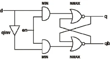
The D Latch circuit is built using MIN gate (OR gate in binary), NMAX gate (AND gate in binary) and quaternary inverters [34, 35] as shown figure 1. When en is equal to logic 3, the latch is open and the output follows the input. When en is equal to logic 0, the latch is closed and the output is held constant. The output of the MIN gate circuit is the input to the NMAX gate. The output of NMAX circuit is the maximum of the 2 inputs. d and q have quaternary logic levels.
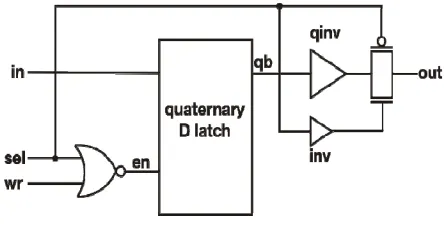
The tristate buffer is implemented by connecting a quaternary inverter in series with a pass transistor as shown in figure 2. The pass transistor used is essentially a PMOS transistor. The gate of the PMOS transistor is connected to sel_l input. Working is as given in table 1.
Table 1: Working of tristate buffer
se_l
PMOS state out0
ON in_bar1
OFF Z2.1. Quaternary SRAM cell
The components as discussed above are put together to build up the Quaternary SRAM cell as shown in figure 3. sel is the select input and wr is the write enable input of the SRAM cell.
When sel = 1, the SRAM cell is disabled and when sel = 0 the SRAM cell is enabled.
Write Operation: During write operation, wr = 0. The output of the NOR gate is logic high. Therefore the latch is enabled. Thus the input is written into the SRAM cell.
Read Operation: During read operation, wr =1. The sel signal of NOR gate is 0. Therefore the latch is disabled. Thus the output is read from the SRAM cell. The table 2 summarizes the working of the SRAM cell
Fig 3: Quaternary single SRAM cell.
Table 2: Working of Quaternary SRAM cell.
.
2.2. Quaternary 1x4 decoder
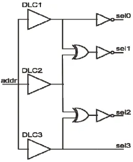
The address decoder is constructed using down literal circuits (DLC) [37], binary xor gates and binary inverters as shown in the figure 4. The truth table for the decoder is as shown in table 3.
Down literal circuits are realized from basic inverter by changing the threshold voltages of pmos and nmos transistors used in the basic inverter. This can be done during the fabrication of the inverter circuit. In the present discussion we will be using 3 different DLC circuits. They are:
DLC1 : Vtp = -2.2V and Vtn = 0.2V. DLC2 : Vtp = -1.2V and Vtn = 1.2V. DLC3 : Vtp = 0.2V and Vtn = 2.2V.
Fig 4: 4x1 decoder.
Table 3: Decoder truth table.
addr sel0 sel1 sel2 sel3
0 0 1 1 1
1 1 0 1 1
2 1 1 0 1
3 1 1 1 0
2.3.Output drivers.
Output drivers are essentially quaternary inverters in the following 4x4 memory array, there are 4 drivers , one for each output line.
2.4.4x4 Quaternary SRAM memory array.
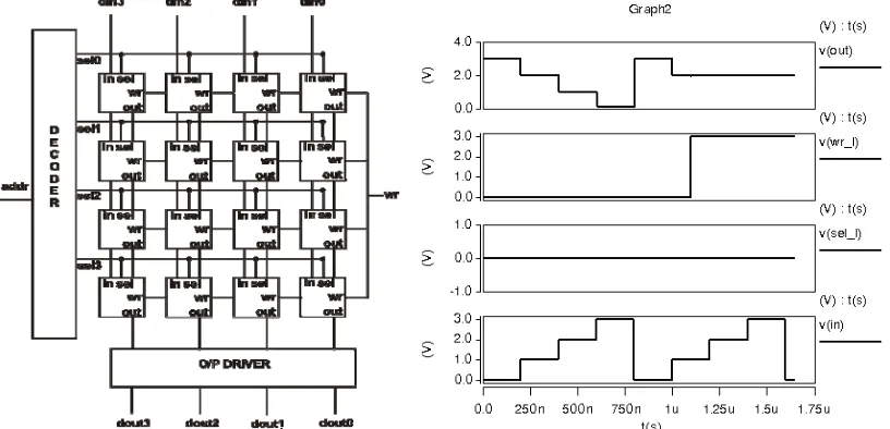
The decoder, driver and 16 SRAM cells are used to realize a 4x4 memory array. The Memory array is as shown in figure 5. Based on the input address, a particular row of SRAM cells are enabled.
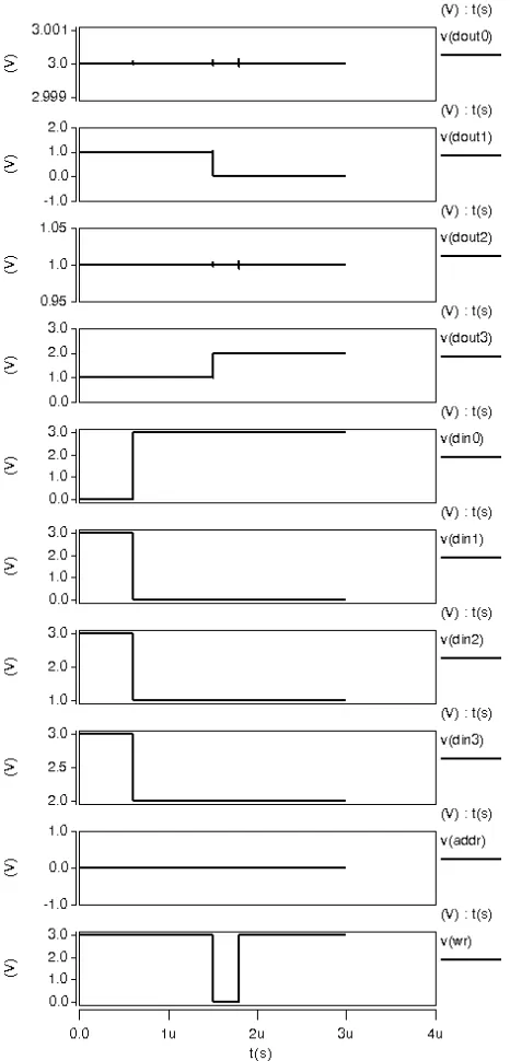
din3, din2, din1, din0 constitute the input data write bus. dout3, dout2, dout1, dout0 constitute the output read bus.
Based on the address on the address line a particular row of SRAM cells are enabled and wr is the write signal.
3. Results and discussion
The above stated SRAM cell and 4x4 array was coded and tested using the tools: Synopsys HSPICE Z-2007.03,
Fig 7: Simulation results Quaternary SRAM 4X4 array.
Table 4: Quaternary Single Static CMOS memory Cell (180nm).
Input Voltage (Volts)
Average Power (Watts) nW
Delay (Wrt Vs Vout) ps
Table 5: Quaternary Single Static CMOS memory Cell (90nm).
.
Table 6: 4x4 array of Quaternary Static CMOS memory Cell (180 nm).
Input Voltage (Volts) Delay (Wrt Vs Vout) ps
0 110.1 1 1.0752 2 460.3 3 621.58
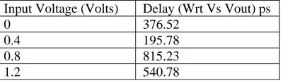
Table 7: 4x4 array of Quaternary Static CMOS memory Cell (90 nm).
Input Voltage (Volts) Delay (Wrt Vs Vout) ps 0 376.52 0.4 195.78 0.8 815.23 1.2 540.78
Table 8: Dynamic Power dissipation, including 4 logic levels and for the whole array (180nm)
Power In µW
Average 58.91
Table 9: Dynamic Power dissipation, including 4 logic levels and for the whole array (90nm).
Power In µW
Average 9.153
Table 10: Proposed 4x4 quaternary SRAM array (180nm).
Table11: Dynamic power dissipation of proposed 4x4 array (180nm).
Table 12: Dynamic power dissipation of binary 4x4 (180nm, 1.2V).
For comparison purpose we have chosen Multiple-valued Static CMOS memory cell [8] and constructed 4X4 array. simulation is carried out at 180 and 90nm technology. Table 4 shows the analysys for single Multiple-valued Static CMOS memory cell at 180nm. Avrage power dissipation is maximum of 226nW when 3V is stored. Delay between write signal and the Vout is in terms of pico secs.
Table 5 shows the analysys of single Multiple-valued Static CMOS memory cell at 90nm. It shows reduction in average power dissipation and delay.
Input Voltage (Volts)
Average Power (Watts)nW
Delay (Wrt Vs Vout)ns
0 2.807 5.531
0.4 0.55 15.427 0.8 3.671 7.105
1.2 11.26 6.161 Input Voltage (Volts) Delay (Wrt Vs Vout)
0 1.145ps
1 83.62ps 2 894.4ps 3 232.86ps
Power In µW
Average 20.45
Power In µW
Table 6 and table 7 shows the respose of output for the write signal in a 4x4 Static CMOS memory Cell array at 180nm and 90nm respectively. Table 8 and table 9 shows the average power dissipation including all 4 logic levels and for the whole array. It is 58.91 µW at 180 nm and 9.153 µW at 90nm.
Proposed 4x4 quaternary SRAM array shown in table 10 is based on quaternary D latch and is simulated using 180nm TSMC technology files. Average power dissipation for the whole array including all four logic levels is given in table 11. It shows 65.28% of improvement in average power dissipation when compared to 4x4 array of Quaternary Static CMOS memory Cell at 180nm. Binary 4X4 memory array with 0 and 1.2 V as two logic levels is constructed and power analysis is given in table 12. Proposed work shows 75% improvement over binary 4X4 array. And also proposed work shows less delay.
4. Conclusion
In this paper, 4X4 quaternary SRAM memory array is designed and simulated using, single 1 to 4 decoder, driver and 16 SRAM cells. SRAM cell is based on quaternary D latch which consists of MIN (AND gate in binary), MAX (OR gate in binary) and quaternary inverter. 4X4 array of quaternary static CMOS memory cell is also constructed and analysed for average power dissipation and propagation delay using 180nm and 90nm technology.Quaternary D latch based SRAM array shows 65.28% of improvement in average power dissipation and reduced propagation delay when compared to 4x4 array of Quaternary Static CMOS memory Cell and 75% improvement over binary 4X4 array at 180nm. Proposed new design is appropriate to be applied for the construction of large low power high performace memory circuit design in quaternary logic and it can work better in the future at higher technology such as 90nm or nano scaling.
References
[1] K. C. Smith, “The prospects for multi-valued logic: A technology and applications view,” IEEE Trans. Computers, vol. C-30, no. 9, pp. 619–634, Sep. 1981.
[2] Michitaka KAMAYAMA, “Toward the age of beyond binary electronic systems”, Proceedings of 20th international symposium multiple-valued logic, pp. 162-166, May 23-25, 1990.
[3] Daniel Etiemble etal.Comparison of Binary and Multivalued ICs according to VLSI criteria, Portal Vol 21 Pages: 28 - 42 April1988.
[4] David A Rich et.al., “A four-State ROM Using Multilevel process Technology”, IEEE Journal of solid Stata circuits, Vol.Sc-19, No 2, April 1984.
[5] Chua-Chin contrast Wang, Proceedings of national Computer Symposium 1995,VLSI Implementation of Multi-Valued Exponential Bidirectional Associative Memory Using Current-mode Circuits. 114-117.
[6] K.W. Current, Memory circuits for Multiple Valued Logic voltage Signals 52 -57 25th IEEE International Symposium on Multiple-Valued Logic 1995.
[7] I. Thoidis et.al Design methodology of Multiple-valued logic Voltage mode storage circuts in Proc. IEEE Int. Symp. Circuits
and Systems, vol. 2, 1998, pp. 125–128.
[8] Ugur Cilingiroglu and Yaman ozelci multiple-valued static CMOS Memory IEEE Transactions on circuits and systems –Analog and digital signal processing. Vol. 48, No 3 march 2001.
[9] Ki-Whan Song et.al Complementary self-Biased Scheme for the robust design of CMOS/SET Hybrid multi-valued logic. Proceedings of the 33rd
IEEE International Symposium on multi-valued logic.(ISMVL 2003).
[10] Shantanu Mahapatra And Adrian mihai Ionescu Realization of Multiple valued logic and memory by hybrid setmos architecture, IEEE Transaction on nanotechnology VOL. 4. No 6, November 2005.
[11] X. Wu and F. Prosser, “Ternary CMOS sequential circuits,” in Proc. 18th
Int. Symp. Multiple-Valued Logic, 1988, pp. 307–313. [12] C. Y. Yu and H. Y. Huang, “Design and application of pipelined dy- namic CMOS ternary logic and simple ternary differential logic,” IEEE J. Solid-State Circuits, vol. 28, pp. 895–906, 1993.
[13] O. Ishizuka, Z. Tan, and H. Matsumoto, “On design of multiple-valued random-access memory,” in Proc. 20th Int. Symp. Multiple-Valued Logic, 1990, pp. 11–17.
[14] I. Thoidis, D. Soudris, I. Karafyllidis, A. Thanailakis, and T. Stouraitis, “Design methodology of multiple-valued logic voltage-mode storage circuits,” in Proc. IEEE Int. Symp. Circuits and Systems, vol. 2, 1998, pp. 125–128.
[15] N. R. Shanbhag, D. Nagchoudhuri, R. E. Siferd, and G. S. Visweswaran, “Quaternary logic circuits in 2- m CMOS technology,” IEEE J. Solid-State Circuits, vol. 25, pp. 790–799, 1990.
[16] K. W. Current, “Voltage mode CMOS quaternary latch circuit,” Elec- tron. Lett., vol. 30, pp. 1928–1929, 1994.
[17] “Memory circuits for multiple valued logic voltage signals,” in Proc. 25th Int. Symp. Multiple-Valued Logic, 1995, pp. 52–57. [18] K. Diawuo and H. Y. Mouftah, “A three-valued CMOS arithmetic logic unit chip,” in Proc. 17th Int. Symp. Multiple-Valued Logic, 1987, pp.215–220.
[19] A. Kramer, V. Hu, C. K. Sin, B. Gupta, R. Chu, and P. K. Ko, “EEPROM device as a reconfigurable analog element for neural networks,” in Tech. Dig. IEEE IEDM, 1989, pp. 259–262.
[20] D. A. Durfee and F. S. Shoucair, “Comparison of floating gate neural network cells in standard VLSI CMOS technology,” IEEE Trans. Neural Networks, vol. 3, pp. 347–353, 1992.
[21] A. J. Montalvo, R. S. Gyurcsik, and J. J. Paulos, “Toward a general-pur- pose analog VLSI neural network with on-chip learning,” IEEE Trans.Neural Networks, vol. 8, pp. 413–423, 1997.
[22] D. Fujita, Y. Amemiya, and A. Iwata, “Characteristics of floating gate device as analog memory for neural networks,” Electron. Lett., vol. 27, pp. 924–926, 1991.
[23] T. Shibata, H. Kosaka, H. Ishii, and T. Ohmi, “A neuron-MOS neural network using self-learning-compatible synapse circuits,” IEEE J. Solid-State Circuits, vol. 30, pp. 913–922, 1995
[25] B. Hochet, “Multivalued MOS memory for variable-synapse neural net- works,” Electron. Lett., vol. 25, pp. 669–670, 1989. [26] R. Castello, D. D. Caviglia, M. Franciotta, and F. Montecchi, “Self re-
freshing analog memory cell for variable synaptic weights,” Electron. Lett., vol. 27, pp. 1871–1872, 1991.
[27] E. Sackinger, E. Boser, J. Bromley, Y. Lecun, and L. D. Jackel, “Application of the ANNA neural network chip to high-speed character recognition,” IEEE Trans. Neural Networks, vol. 3, pp. 498–505, 1992.
[28] Y. Arima, M. Murasaki, T. Yamada, A. Maeda, and H. Shinohara, “A refreshable analog VLSI neural network chip with 400 neurons and 40K synapses,” IEEE J. Solid-State Circuits, vol. 27, pp. 1854–1861, 1992.
[29] T. Watanabe, K. Kimura, M. Aoki, T. Sakata, and K. Ito, “A single 1.5 V digital chip for a 10 synapse neural network,” IEEE Trans. Neural Networks, vol. 4, pp. 387–393, 1993.
[30] B. Linares-Barranco, E. Sanchez-Sinencio, and A. Rodriguez-Vazquez, “A CMOS analog adaptive BAM with on-chip learning and weight refreshing,” IEEE Trans. Neural Networks, vol. 4, pp. 445–455, 1993.
[31] T. Morie and Y. Amemia, “An all-analog expandable neural network LSI with on-chip backpropagation learning,” IEEE J. Solid-State Circuits, vol. 29, pp. 1086–1093, 1994.
[32] M. Verleysen, B. Sirletti, A. M. Vandemeulebroecke, and P. G. A.Jespers, “Neural networks for high-storage content-adressable memory: VLSI circuit and learning algorithm,” IEEE J. Solid-State Circuits, vol.24, pp. 562–569, 1989.
[33] P. G. Hollis and J. J. Paulos, “Artificial neural networks using MOS analog multipliers,” IEEE J. Solid-State Circuits, vol. 25, pp. 849–855,1990.
[34] R. Coggins, M. Jabri, B. Flower, and S. Pickard, “A hybrid analog and digital VLSI neural network for intracardiac morphology classification,” IEEE J. Solid-State Circuits, vol. 30, pp. 542–549, 1995.
[35] Ricardo Cunha G. da Silva et.all , “A Novel Voltage Mode CMOS Quaternary Logic Design” , IEEE Transactions on Electron Devices , vol.53, no. 6 , June 2006.
[36] Vasundara Patel K. S, K. S. Gurumurthy, “Quaternary CMOS Combinational Logic Circuits”, International conference on semiconductor technology in conjunction with ICIMT 2009, pp.538 - 548.