Analysis of Various Parameters of Memory Devices
Deiva Jothi Hepzibah.D 1, Divya Prabha. P2, Gomathi.M3, Gokul. G4 and Dhanasekar. J5
1,2,3,4UG Students, Department of ECE, Sri Eshwar College of Engineering, Coimbatore, Tamilnadu, India. 5Assistant Professor, Department of ECE, Sri Eshwar College of Engineering, Coimbatore, Tamilnadu, India.
Article Received: 24 January 2018 Article Accepted: 27 February 2018 Article Published: 08 April 2018
1.INTRODUCTION
It is hard to imagine a world without semiconductor storage devices. Since the first practical device, a transistor,
was built in 1947, activity in this area has flourished. We are now surrounded by semiconductors, and rely on their
use in everyday commercial devices. The expanse of the semiconductor industry is testimony to the value of the
research into their fundamental physics, materials and technology. Now in the major classification of this SRAM
we have RAM and ROM. Thus we could make them act in synchronous or asynchronous manner to attain
read/write operation. In Single port memories only one operation either read or write can be done for a given clock
pulse. In dual port memories separate clocks for read and write operations will be there which can be used for
simultaneous read and write operations. The detailed contents of the classification of memory are given below.
2. LITERATURE REVIEW
I. CONTENT ADDRESSABLE MEMORY
Content-addressable memory (CAM) is computer memory that operates like a hardware search engine for
search-intensive applications. Content-addressable memories (CAMs) are hardware search engines that are much
faster than algorithmic approaches for search-intensive applications. CAMs are composed of conventional
semiconductor memory (usually SRAM) with added comparison circuitry that enable a search operation to
complete in a single clock cycle. The two most common search-intensive tasks that use CAMs are packet
forwarding and packet classification in Internet routers. CAM is capable of searching its entire contents in a single
clock cycle. It does that by pairing the SRAM-based memory with additional logic comparison circuitry that that is
active on every clock cycle. The way CAM functions is almost the opposite of random access memory (RAM). To
retrieve data residing on RAM, the OS provides the memory address where the data is stored. Data stored on CAM,
on the other hand, can be accessed by searching for the content itself, and the memory retrieves the addresses where
that content can be found. Because of its parallel nature, CAM is much faster than RAM for searching. Ternary
CAM (TCAM) adds a third state to RAM, beyond binary, for a wildcard functionality that provides for variable
A B S T R A C T
Semiconductor memory is an electronic storage device, implemented on a semiconductor-based integrated circuit. It is made in many different types and technologies. Most modern semiconductor memory devices are implemented allowing random access, which means that it takes the same amount of time to access any memory location, so data can be efficiently accessed in any random order. In this paper various types of memory circuits such as Content Addressable Memory (CAM), Single port RAM synchronous Read/ Write, Single port RAM asynchronous Read/ synchronous Write, Single port RAM asynchronous read/write, Dual Port RAM synchronous Read/ Write, Dual Port RAM asynchronous Read/ Write, Conventional 6-T SRAM and Adiabatic SRAM are analyzed and the parameters are analyzed using Xilinx ISE 12.1.
characters in searches and adds additional complexity to the circuits. Because of their low capacities, high power
usage and consequent heat dissipation requirements, CAM and TCAM remain isolated to specialized applications
such as Internet routers and switches, where they increase the speed of route look-up, packet classification, packet
forwarding and access control list-based commands.
Binary CAM Cell
Binary CAMs support storage and searching of binary bits, zero or one (0,1). Fig 1 Shows the structure of binary
CAM cell which is used for storing and retrieving the data.
Fig 1 Binary CAM cell
Ternary CAM cell
Ternary CAMs support storing of zero, one, or don't care bit (0,1,X). Ternary CAMs are presently the dominant
CAM since longest-prefix routing is the Internet standard. Fig 2 depicts the basic structure of Ternary CAM cell.
Fig 2 Ternary CAM cell
II. SINGLE PORT RAM SYNCHRONOUS READ/WRITE
Simultaneous read-write is defined as the situation when the two clocks, CLKA and CLKB, turn on very close to
one another to initiate one write operation and one read operation on the same address of the RAM. The behavior in
a read-write or a write-read situation depends on what occurs at the positive or the opening edge of the clock. Since
it takes time for the write operation to occur and also the read operation, a small delay is required between the
positive edges of CLKA and CLKB in order to successfully perform simultaneous write-read or read-write
operations. All events except for events having both edges opening simultaneously will have a stable, known
III. SINGLE PORT SRAM ASYNCRONOUS READ AND WRITE
Asynchronous I/O, or Non-sequential I/O is a form of input/output processing that permits other processing to
continue before the transmission has finished. Input and output (I/O) operations on a computer can be extremely
slow compared to the processing of data. An I/O device can incorporate mechanical devices that must physically
move, such as a hard drive seeking a track to read or write; this is often orders of magnitude slower than the
switching of electric current. For example, during a disk operation that takes ten milliseconds to perform, a
processor that is clocked at one gigahertz could have performed ten million instruction-processing cycles. A simple
approach to I/O would be to start the access and then wait for it to complete. But such an approach (called
synchronous blocking I/O) would block the progress of a program while the communication is in progress, leaving
system resources idle. When a program makes many I/O operations (such as a program mainly or largely dependent
on user input), this means that the processor can spend almost all of its time idle waiting for I/O operations to
complete.
DUAL PORT RAM SYNCHRONOUS READ/WRITE
Dual-Port RAM (DPRAM) is a type of Random Access Memory that allows multiple reads or writes to occur at the
same time or nearly the same time, unlike Single-Port RAM which only allows one access at a time.
IV. DUAL PORT RAM ASYNCHRONOUS READ/WRITE
Asynchronous dual-port RAM responds to address and control pin inputs without the need for a clock. A simplified
asynchronous dual port RAM device. The device interface includes two ports, each of which has a set of signals:
address, data, and control. Each signal has either the subscript L or R to designate left or right, respectively. The
address pins are unidirectional inputs to the device. Their states specify the memory location to be read from or
written to.
V. SYNCHRONOUS FIFO
In synchronous FIFO, we use only single clock that controls both write and read operations. It means that both write
and read operations are synchronous to each other. So, it is called as synchronous FIFO.
VI. ASYNCHRONOUS FIFO
Inasynchronous FIFO, we use two clocks that is write clock and read clock, write clock will take care of write
operation and read clock will take care of read operation. It means that both write and read operations are
asynchronous to each other. So, it is called as asynchronous FIFO.
3. EXISTING METHOD
Conventional 6- T SRAM
A typical SRAM cell I s made up of six MOSFETs as shown in fig 1. Each bit in an SRAM is stored on four
which are used to denote 0 and 1. Two additional access transistors serve to control the access to a storage cell
during read and write operations. In addition to such six-transistor (6T) SRAM, other kinds of SRAM chips use 4,
8, 10 (4T, 8T, 10T SRAM), or more transistors per bit.
Fig 3 Conventional 6-T SRAM
SRAM cell has three different states: standby (the circuit is idle), reading (the data has been requested) or writing
(updating the contents). SRAM operating in read mode and write modes should have "readability" and "write
stability", respectively. The three different states work as follows:
Standby:-If the word line is not asserted, the access transistors M5 and M6 disconnect the cell from the bit lines.
The two cross-coupled inverters formed by M1 – M4 will continue to reinforce each other as long as they are
connected to the supply.
Read:-In theory, reading only requires asserting the word line WL and reading the SRAM cell state by a single
access transistor and bit line, e.g. M6, BL. Nevertheless bit lines are relatively long and have large parasitic
capacitance. To speed-up reading, a more complex process is used in practice: The read cycle is started by
recharging both bit lines BL and BL, i.e. driving the bit lines to a threshold voltage (midrange voltage between
logical 1 and 0) by an external module (not shown in the figures). Then asserting the word line WL, enabling both
the access transistors M5 and M6 which causes the bit line BL voltage to either slightly drop (bottom NMOS
transistor M3 is ON and top PMOS transistor M4 is off) or rise (top PMOS transistor M4 is on). It should be noted
that if BL voltage rises, the BL voltage drops, and vice versa. Then the BL and BL lines will have a small voltage
difference between them. A sense amplifier will sense which line has the higher voltage and thus determine
whether there was 1 or 0 stored. The higher the sensitivity of the sense amplifier, the faster the read operation.
Write:-The write cycle begins by applying the value to be written to the bit lines. If we wish to write a 0, we would
apply a 0 to the bit lines, i.e. setting BL to 1 and BL to 0. This is similar to applying a reset pulse to an SR-latch,
which causes the flip flop to change state. A 1 is written by inverting the values of the bit lines. WL is then asserted
and the value that is to be stored is latched in. This works because the bit line input-drivers are designed to be much
cross-coupled inverters. In practice, access NMOS transistors M5 and M6 have to be stronger than either bottom
NMOS (M1, M3) or top PMOS (M2, M4) transistors. This is easily obtained as PMOS transistors are much weaker
than NMOS when same sized. Consequently when one transistor pair (e.g. M3 and M4) is only slightly overridden
by the write process, the opposite transistors pair (M1and M2) gate voltage is also changed. This means that the
M1 and M2 transistors can be easier over ridden, and so on. Thus, cross-coupled inverters magnify the writing
process.
4. COMPARISON OF VARIOUS MEMORY CIRCUITS
For the various memory circuits like Single Port RAM Synchronous Read/Write, Single Port SRAM Asynchronous
Read and Write, Dual Port RAM Synchronous Read and Write, Dual Port RAM Asynchronous Read and Write,
Synchronous FIFO, Asynchronous FIFO, Content Addressable Memory the following parameters are analyzed
using Xilinx 12.1 i) Temperature ii) Power iii) Junction Temperature iv) Number of bonded IOBs v) IOB Flip
Flops vi) Memory Usage vii) Delay.
5. RESULTS AND DISCUSSION
Various types of memory circuits such as Content Addressable Memory (CAM), Single port RAM synchronous
Read/ Write, Single port RAM asynchronous Read/ synchronous Write, Single port RAM asynchronous
read/write, Dual Port RAM synchronous Read/ Write, Dual Port RAM asynchronous Read/ Write, Conventional
6-T SRAM and Adiabatic SRAM are analyzed and the parameters are analyzed using Xilinx ISE 12.1 and the
values of each parameters are tabulated in table 1 and are shown below.
Table 1 Comparison of various parameters of the Memory Circuits
PARAMETERS
SINGLE PORT RAM SYNCHRONOUS
READ/WRITE
SINGLE PORT SRAM ASYNCHRONOUS READ
AND WRITE
DUAL PORT RAM SYNCHRONOU
S READ AND WRITE
DUAL PORT RAM ASYNCHRONO
US READ AND WRITE
SYNCHRONOUS FIFO
ASYNCHRONOUS
FIFO CAM
Temperature 25C 25C 25C 25C 25C 25C 25C
Power 0.052W 0.0527W 0.0527W 0.0527W 0.0527W 0.0527W 0.052W
Junction
Temperature 27.5 27.5 27.5 27.5 27.5 27.5 27.5
Number of bonded IOBs
(utilization)
21% 21% 42% 41% 17% 20% 11%
IOB Flip
Flops 8 _ 2064 2048 25 2048 9
Memory Usage 197980kb (193.33mb) 198108kb (193.464mb) 218268kb (213.132mb) 569308kb (555.96mb) 188316kb (183.90mb) 212572kb
(207.58mb) 108mb
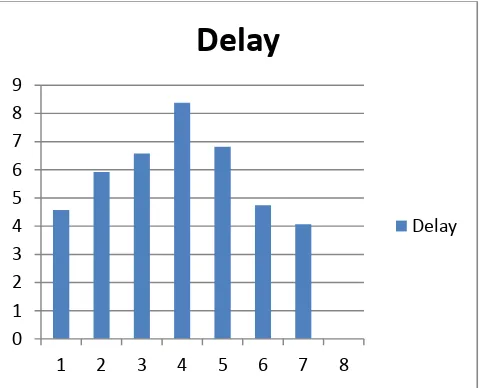
Memory usage and delay comparison are done for the memory circuits and are shown below.
Fig 4 Memory Usage Comparison for different circuits
Fig 5 Delay Comparison for different circuits
6. FUTURE SCOPE
From the table we can come to a conclusion that the delay is reduced in CAM and hence we can use in application
like data compression and encryption, pattern recognition, normal SD card. This will result in increased efficiency
when compared to the former design.
REFERENCES
[1] J. Dhanasekar, “A Study on Conventional SRAM and Adiabatic SRAM” , International Journal of Scientific
Research in Science, Engineering and Technology, 2017.
[2] “Cypress, Understanding Synchronous Dual-Port RAMs”, Document Number: 001-17358, 2017.
0 100 200 300 400 500 600
1 2 3 4 5 6 7
Memory usage
Memory usage
0 1 2 3 4 5 6 7 8 9
1 2 3 4 5 6 7 8
Delay
[3] Russell Tessier, Vaughn Betz, David Neto, Thiagaraja Gopalsamy, “Power-aware RAM Mapping for FPGA
Embedded Memory Blocks”, July 2015.
[4] L. Benini, A. Macii, and M. Poncino, “ A recursive algorithm for low-power memory partitioning” , In
Proceedings of the International Symposium on Low Power Electronics and Design, Rapallo, Italy, July, 2000, pp.
78-83.
[5] Qutaiba Ali, “A Flexible Design of Network Devices Using Reconfigurable Content Addressable Memory” ,
The International Arab Journal of Information Technology, Vol. 8, No. 3, July 2011.
[6] Jonathan Schrock, Alex J. McCaskey, Kathleen E. Hamilton ID, Travis S. Humble * ID and Neena Imam,
“Recall Performance for Content-Addressable Memory Using Adiabatic Quantum Optimization”, 15 September
2017.
[7] David Andrew Roberts, “Efficient Data Center Architectures Using Non-Volatile Memory and Reliability
Techniques”, the University of Michigan 2011
[8] Mark Horowitz, Elad Alon, Dinesh Patil, “Scaling, Power, and the Future of CMOS”, Jan 2011.
[9] Zamin Ali Khana, S. M. Aqil Burneyb, , Jawed Naseemc, Kashif Rizwand, “Optimization of Power
Consumption in VLSI Circuit”, IJCSI International Journal of Computer Science Issues, Vol. 8, Issue 2, March
2011.
[10] Nisha Sharma, Manmeet Kaur, “A Survey of VLSI Techniques for Power Optimization and Estimation of
Optimization” ,International Journal of emerging technology and advanced engineering, Volume 4, Issue 9,
September 2014.
[11] Akanksha Trigun,” Pass Transistor for adiabatic logic for low power VLSI power design” , October 2011.
[12] Santanu Duta,” ASAP: A Transistor Sizing Tool for Speed, Area, and Power Optimization of Static CMOS