Int. J. Nanosci. Nanotechnol., Vol. 12, No. 1, March. 2016, pp. 55-69
Short Communication
Presenting a New Efficient QCA Full Adder
Based on Suggested MV32 Gate
A. Safavi and M. Mosleh*
Department of Computer Engineering, Dezful Branch, Islamic Azad University, Dezful, I.R.Iran
(*) Corresponding author: [email protected]
(Received: 19 May 2015 and Accepted: 20 Feb. 2016)
Abstract
Quantum-dot Cellular Automata (QCA) technology is a solution for implementation of the nanometer sized circuits and it can be a suitable replacement for CMOS. Similar to CMOS technology, designing the basic computational element such as adder with the QCA technology is regarded as one of the most important issues that extensive researches have been done about it. In this paper, a new efficient QCA full adder based on proposed MV32 gate is introduced which its novel structure leads to proper design technique selection and also its arrangement makes it very suitable. The proposed QCA full adder has 31 cells and its outputs are generated after the 0.75 of a clock time period. The proposed full adder is simulated using the QCADesigner2.0.3 simulation tool and has been compared with former works. The simulation results show that the proposed QCA full adder in terms of the number of used cells and occupied area is so better than others.
Keywords:Majority gate, MV32 QCA gate, Quantum-dot Cellular Automata (QCA), QCA full adder.
1. INRODUCTION
Decreasing the size of the CMOS transistors is very difficult at nanometer scale. The QCA technology can be viewed as an alternative technology. Dense Nanometer sized circuits can be designed with low power consumption and low delay time in the QCA scope. The QCA circuits and their implementation process aren't involved with the conventional lithography and load depletion challenges. The recent QCA circuits are not capable to have functionality in high temperatures because of quantum challenges but this problem will be solved in future. Therefore, the quantum computers and devices can be used in future. One of the main applications for the electronic circuits is implementation of digital computer circuits such as the arithmetic and logic unit (ALU) and other important parts of the central processing unit (CPU). The full adder is the main building block for many
arithmetic circuits. Designers of the QCA circuits try to reduce the delay time, circuits’ occupied area and the number of used cell. Generally a 1-bit full adder has three inputs which are A, B and Cin for producing the Sum and the Cout for outputs. A number of algebra equations can be used to show how the outputs of the full adder are generated. An algebra equation is composed of some algebra operators and some input variables; also each algebra operator points to a QCA gate. The equations used by Wang-Walus are selected to be implemented by utilizing some methods(Wang et al., 2003).
combined for generating the Sum and the
Cout outputs.
The rest of paper is organized as follows. Section 2 contains the basics for QCA technology, the fundamentals of QCA logical gates, clocking for QCA circuits, the crossover connections and also the proposed MV32 cellular structure as a new useful QCA structure. At section 3, the structure of former works on the QCA full adder scope will be described and their problems or efficiencies will be addressed. At section 4, two new QCA full adders with 1 and 3 layers using the MV32 gate are proposed. Then, at section 5, the simulation results for the proposed QCA full adders will be mentioned and also this section compares them with former QCA full adders. Finally conclusion of the paper will be made at the last section.
2. PRELIMINARIES 2.1. QCA Cell
QCA circuits are constructed using a basic and simple element that is QCA cell. The QCA cell is a nanometer structure like a square that has four quantum-dots and these Quantum-dots are placed at four corners of each QCA cell. A quantum-dot is a nanometer sized structure that is used for trapping the electrons in the three dimensional space. A quantum-dot is constructed from a conductive material that is surrounded by some insulating materials. If an electron enters into a quantum-dot, it can’t escape from the quantum-dot without enough electrical potential. Two extra electrons intruded into QCA cell and these electrons have the ability of tunneling between the quantum-dots. The repelling force of electrons moves the charge to the opposite corners of QCA cell. Each quantum-dot has a certain polarity and the polarity of the cell can be calculated using these polarities based upon Eq.1. The electrons of the cell can include two possible arrangements which lead generating two polarities for QCA cell. These two polarities represent the binary 0 and binary 1. Four
quantum-dots are connected using tunnel junctions and the voltage of the tunnel junction can be controlled to enable or disable the electron tunneling. This effect creates the clocking possibility for QCA cells. Two types of QCA cells are used in QCA circuits entitled the normal cell and the diagonal cell (see Figure.1).
P=(𝑝2+𝑝4)−(𝑝1+𝑝3)𝑝1+𝑝2+𝑝3+𝑝4 (1)
` 1
2 3 4
P=+1(logic 1) P=-1(logic0) ` 1
2 3 4 ` 1
2 3 4
Null
(a)
P=-1(logic 0) 1
2 3
4
1 2 3
4
P=+1(logic 1)
1 2 3
4
Null
(b)
Figure.1. (a) Normal QCA cell, (b) diagonal QCA cell
2.2. QCA Wires and gate
Another basic QCA gate is the 3-input majority gate (MV3). The logic symbol and the cellular implementation for a 3-input majority gate are shown in Figure. 2(c).The Algebra equation for the 3-input majority gate is according to Eq. 2. In QCA scope, the 2-inputs logic AND gate and the 2-inputs logic OR gate can be implemented using the 3-input majority gate. Therefore, the conventional logic equations which are constructed using AND and OR operators can be translated to QCA logic equations using the inverter and majority operators and some algebra manipulations. Another basic QCA gate is the 5-input majority gate (MV5) that can be used in QCA designs which is also a useful gate. The algebra equation for the 5-input Majority gate is performed based upon Eq.3. This QCA gate can be implemented with some cellular structures. A simple cellular implementation for this QCA gate is shown in Figure. 2(d).
MV3 (A,B,C)=AB+BC+AC (2)
MV5(A,B,C,D,E)=
ABC+ABD+ABE+ACD+ACE+ ADE+BCD+BCE+BDE+CDE
(3)
2.3. Clock Pulse in the QCA
Unlike the clock pulse in CMOS circuits, which consists of an upper phase and a lower phase, the clock pulse in QCA technology has four working phases. The clock pulse mechanism in QCA technology gives computation permission to a array and then it blocks the sub-array as well as polarization of output cell sets as an input for next sub-array. The phase change is assumed as the potential change and the clock pulse phases include four states: Switch, Release, Hold and Relax. Four zones of the clock pulse and the way that all the information in a QCA wires which can be propagated under influence of clock pulse can be seen in Figure.3.
` ` ` ` `
IN IN
Normal QCA wire
IN IN
Diagonal QCA wire (a)
IN OUT=NOT (IN)
Inverter gate using the diagonal QCA wire
` `
` `
IN
OUT=NOT (IN)
Simple inverter gate (b)
MV3 A B
C OUT=MV3(A,B,C)
` `
`
` `
B
A
C
OUT
MV5 A B C
OUT=MV5(A,B,C,D,E) D
E
` `
`
`
`
E C
B
OUT
` `
` `
`
D A
(c) (d)
Time
Switch Hold Releas Relax
Switch Hold Releas Relax
(a) Four time zones for the clock pulse in QCA and their effects on a cell.
Dataflow
Phase 0 clock pulse Phase 1 clock pulse Phase 2 clock pulse Phase 3 clock pulse
Input Output
(b) How information is spread in a QCA wire
Figure3. Timing of the clocking signals
2.4. Coplanar Crossover and Multilayer Crossover Connection
At complicated QCA circuits, two possible ways for propagating the signals and reducing the circuit’s occupied area exist. One of these ways uses the coplanar crossover connections. As shown in Figure. 4(a), the coplanar connection uses a diagonal wire which passes across the normal wires. The normal wires have two sections. It is possible for those of signals which propagate across the normal wires to be destroyed because of the distance between its sections. Good signal transformation in coplanar crossover connections requires placing both the diagonal wire and the first section of the normal wire at a same clock zone and place the second section of the normal wire at the next clock zone. It is possible to route the wires of a QCA circuit in one layer using the coplanar crossover wires. A better way for passing a QCA wire across the obstacle wires or circuits is the multilayer crossover connections. This should be noted that the multilayer electrical circuits do exist. When the routing wires of an electrical circuit are complicated, the multilayer circuits can be utilized for connecting the layers using VIA. A VIA is a hole that can connect to
layers or two separate boards. Using this technique leads building the multilayer electrical boards. A number of former QCA full adders would be described at the next section which uses the multilayer connections. Also, this method can be performed for the proposed QCA full adder. A multilayer crossover connection is shown in Figure. 4(b).The vertical cells are marked by a circle on their surfaces and can be placed at all layers. To route a QCA wire towards an upper or a lower layer, the vertical QCA cells are used. These cells can propagate the signals to their four sides plus their upper and lower surfaces. A vertical cell works like a VIA. Another type of QCA cells is the crossover cells. These cells are marked by a ‘×’ sign on their surface and can be placed at the upper layers of the circuit. This is possible to place the crossover and the vertical cells at the upper layers. Some intermediate layers between two neighbor layers must be placed. The intermediate layers just contain the vertical cells.
(a)
(b)
Figure4. (a) Coplanar crossover connection, (b) Multilayer crossover
2.5. Proposing the MV32 Structure and Some of its Applications
In this section, designing the proposed MV32 structure is described. The simple inverter gate and the 3-input majority gate would be described later. These basic gates can be combined to obtain another gate that acts like a 3-input majority gate but it has 2 clock pulse phases. This structure produces OUT1 signal and it is shown in Figure. 5(a). The placement of output cells can vary to obtain another similar structure that produces the OUT2 signal and it is shown in Figure. 5(b).
(a)
(b)
Figure5. (a) First part of the MV32, (b) Second part of the MV32
At this point, the structure is examined firstly that is shown in Figure. 5(a). At the first clock zone (the clock zone 0), the cells which are marked with 1, 2, 4, 5, 6 and 7 go to the Switch state. Then the A
input polarity is copied to cell 5, B input polarity is copied to cell 2 and the Cin
input polarity is copied to cell 7. At the clock zone1, the cells 2, 5 and 7 go to the Hold state and sustain their polarity and also they can influence their neighbors cells which are placed at clock zone 1.The cells 3, target cell and the cell OUT1 are at clock zone 1 go to the switch state and obtain their polarities via the sum of the forces which come from the neighbor cells. The cells 3, target cell and the OUT1 form a simple inverter gate. The polarity of cell 3 can be calculated as MV3 (A, B, Cin) that
transmits the inverse of its polarity (𝑀𝑉3(𝐴, 𝐵, 𝐶𝑖𝑛) ) to the target cell. So, the target cell is influenced by 3 forces from the cells 3, 2 and 5 which are its neighbors. These forces are represented by f1=A,
f2=B and f3=𝑀𝑉3(𝐴, 𝐵, 𝐶𝑖𝑛 ). The polarity of the target cell can be calculated by Eq. 4.
The second structure which is shown in Figure. 5(b), works in a same manner. The polarity of cell 3 is calculated as MV3 (A, B, Cin) and the polarity of the target cell and OUT2 can be calculated using Eq. 5.
(4)
OUT1=target cell polarization =MV3(𝑀𝑉(𝐴, 𝐵, 𝐶𝑖𝑛) ,A,B)
=MV3((𝐴 𝐵 + 𝐶𝑖𝑛 𝐵 +𝐴 𝐶𝑖𝑛 ),A,B) =B𝐶𝑖𝑛 +AB+𝐶𝑖𝑛 𝐴 = 𝑀𝑉3 𝐴, 𝐵, 𝐶𝑖𝑛
(5)
OUT2=target cell polarization =MV3 (𝑀𝑉(𝐴, 𝐵, 𝐶𝑖𝑛) , A, Cin)
=MV3((𝐴 𝐵 + 𝐶𝑖𝑛 𝐵 +𝐴 𝐶𝑖𝑛 ), A, Cin)
=A𝐵 +ACin+𝐵 𝐶𝑖𝑛 = 𝑀𝑉3(𝐴, 𝐵 , 𝐶𝑖𝑛)
Now, these two parts can be combined to obtain a structure that produces the OUT1
and OUT2 simultaneously. This final
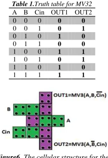
structure is the MV32 gate. It is desirable to find a structure that can help to design a new efficient QCA full adder. This structure is called the MV32 because it acts like the majority gates and it has 3 inputs and 2 outputs. The MV32 QCA structure has 11 QCA cells. The structure of this gate can be seen in Figure. 6 and its truth table can be seen in Table 1.The outputs of this cellular structure implement two majority gates. This cellular structure has two clock pulse phases
One of the most important application of the proposed MV32 gate is the capability of producing AND, OR logics simultaneously, with lower number of cells. For this purpose, one of the inputs of the MV32 structure is forced at logic 0 and logic 1 and calculates the OUT1 and OUT2
simultaneously. Just the results of changing the Cin input are shown because the output logic has no changes in other cases by changing the A and B input lines.
Table 1.Truth table for MV32
OUT2 OUT1
Cin B A
0 0
0 0 0
1 0
1 0 0
0 1
0 1 0
0 0
1 1 0
1 1
0 0 1
1 0
1 0 1
0 1
0 1 1
1 1
1 1 1
Figure6. The cellular structure for the MV32
These results are shown in Figure. 7(a) and Figure. 7(b), respectively. So, the AND, OR logics can be considered simultaneously and this is so helpful to design a wide variety of QCA circuits. To produce the A+B and A𝐵 functions by using 3-input majority gate, 19 QCA cells are required. This implementation can be seen in Figure. 7(c). These two functions can be produced using the proposed MV32 with just 11 QCA cells.
3. FORMER WORKS ON QCA FULL ADDERS
The former works on QCA full adder is described in this section. As mentioned later, a full adder has three inputs A, B and
Cin which produces two outputs named
Sum and Cout. The algebra equations for generating the Sum and Cout are based on the Eq. 6 and Eq.7. These equations describe the generation of outputs of a full adder in conventional logic circuit scope.
Sum=ABCin (6)
Cout=A.B+B.Cin+Cin.A
=MV3(A,B,Cin) (7)
(a)
(b)
(c)
Figure7. (a) and (b) produce the simultaneous AND, OR logics by changing
the Cin input using MV32, (c) produce the simultaneous AND, OR logic without using
MV32
the Sum and Eq. 9 for the Cout outputs would be obtained. Thus, the complexity of the equations would be reduced at this step. This reduction in complexity of the equations will reduce the number of used gates and cells and occupied area of the full adder’s cellular circuit.
Sum=MV3(MV3(A,𝐵 ,Cin),MV3(A, B,
𝐶𝑖𝑛
), MV3(𝐴 , B,Cin)) (8)
Cout=MV3 (A, B, Cin) (9)
3.1. WANG-WALUS QCA Full Adder To obtain the Eq. 10, Eq. 8 can be changed to achieve at a better logic function for generating the Sum output. This equation is proposed by Wang and Walus(Wang et al., 2003). In this kind of QCA full adder, the algebra equation for generating the Cout output is based upon Eq. 9.
Sum=MV3(MV3(𝐴 , 𝐵, 𝐶𝑖𝑛 ),MV3 (A,B,𝐶𝑖𝑛 ), 𝐶𝑖𝑛 )
(10)
In this work, the coplanar crossover connections are used to transmit the input signals to the core of the QCA full adder. The QCA cellular structure for this design is shown in Figure. 8. This QCA full adder has 5 clock pulse phases of delay time (1.25 of clock cycles) and can be implemented by 145 cells and 0.17 μm^2 of occupied area. This QCA full adder has up to 140 cells because of employing many coplanar crossover connections. In Figure. 8, the input wire A is passed across the wires B and Cin through the {a1-a2-a3}
and {a4-a5-a6} paths. Similarly, the input wire B is passed across the Cin wire through the {b1-b2} and {b3-b4} paths. The input signals may or may not be inverted across these paths.
3.2. CHO’S QCA Full Adder
Another QCA full adder that uses the Eq. 10 for generating the Sum output is the Cho’s QCA full adder(Cho and Swartzlander Jr, 2009). The Cho’s design is shown in Figure. 9. This full adder is
implemented by using 86 cells and occupies 0.11 μm^2 of area. The main efficiency of the Cho’s QCA full adder is the technical branches from the Cin input signal. The Cin input signal enters the core of the full adder cellular circuit and takes three branches from its input path.
Figure8. Wang and Walus QCA full adder logic circuit(Wang et al., 2003)
Figure9. Cho’s QCA full adder cell layout(Cho and Swartzlander Jr, 2009)
These branches facilitate the implementation of the majority functions of the Eq. 10 which produce the Sum
output, because the Cin signal and its inverse signal are combined with other inputs at three points in this circuit. These branches are shown in Figure. 9. Of course, the input wire A, is connected to
the MV3 (A, B, Cin) function through a
multilayer crossover wire and the function
wire. These techniques altogether optimize the Cho’s QCA full adder on the number of cells and delay factors.
3.3. AZGHADI’S QCA Full Adder Azghadi’s QCA full adder (Azghadi et al., 2007) led to a revolution in the QCA full adder’s world because of facilitating the generation of Sum output using the 5-input majority gate. This full adder can be considered in Figure. 10 and the algebra equations for this full adder perform according to Eq. 11 and Eq. 12.
Cout=MV3(A,B,Cin) (11)
Sum=MV5(A,B,Cin,𝐶𝑜𝑢𝑡 ,𝐶𝑜𝑢𝑡 ) (12)
The output of the 3-input majority gate produces the Cout and then the Cout signal combines with the remaining gates of the full adder for generating the Sum output. This architecture is efficient because of the low number of QCA gates. The logic circuits for some QCA full adders such as Hashemi’s QCA full adder are based on the structure of Azghadi’s QCA full adder. Note that the Azghadi’s paper has not proposed any cellular structure for this kind of full adder. This full adder is important in the matter of logic circuit point of view.
Figure10. Azghadi’s QCA full adder
(Azghadi et al., 2007)
3.4. HASHEMI’S QCA Full Adder One of the new QCA full adders is the Hashemi’s QCA full adder (Hashemi et al., 2012). This design is shown in Figure. 11(b) and uses the Azghadi’s logic circuit to produce the Sum and Cout. Hashemi et al. proposed a new cellular structure for the 5-input majority gate that is shown in Figure. 11(a). This design uses 51 cells and
has three clock pulse phases (0.75 of a clock period) and its occupied area is equal to 0.04 μm^2. The multilayer crossover connections and efficient algebra equations optimize this design in the matter of occupied area and the number of cells properties.
(a)
(b)
Figure11. (a) proposed 5-input majority gate by Hashemi, (b) Hashemi’s
QCA full adder (Hashemi et al., 2012)
3.5. NAVI’S QCA Full Adder
Another QCA full adder is the Navi’s QCA full adder (Navi et al., 2010). The logical circuit of this full adder is similar to Azghadi’s QCA full adder but it has two inverter gates and one 3-input majority gate and one 5-input majority gate. As shown in Figure. 12, the multilayer connections are used in this design and the occupied area equals to 0.05 μm^2. This design has 73 cells and three clock pulse phases.
(a)
(b)
Figure12. Navi’s QCA full adder (Navi et al., 2010) (a) logical design, (b) cell layout
We believe that the proposed cellular structure for this full adder is wrong and this circuit cannot work and cannot be simulated correctly. This would prove that the results of the Sen’s paper are wrong. The logic circuit for this full adder is based on Azghadi’s work but in this work the simple 5-input majority gate (one layer gate) must be replaced by a multilayer 5-input majority gate (5-layer-5-input majority). The proposed cellular structure for this gate is shown in Figure. 13. This multilayer gate is an extended 3-input majority gate that takes two extra inputs from the upper side and the lower side layers (D and E inputs in Figure. 13).
Figure13. five layers for the multilayer 5-input majority gate
The cellular structure for the Sen’s proposed QCA full adder is presented in the corresponding paper as Figure. 14 illustrates. This cellular structure is implemented using 34 cells and has just 3
layers. By simulating this cellular structure using the QCADesigner 2.0.3 software, this would be revealed that it cannot work and cannot produce the Sum output. If a QCA full adder uses the 5-layer-5-input majority gate, then its cellular structure must be implemented using 5 layers. Due to the logical circuit (that is the Azghadi’s logic circuit for the full adder) for this full adder, the output of the 3-input majority gate that presents the Cout signal must be inverted and then takes two branches. Then these two branches must be connected to the 5-input majority gate. One of these branches must be connected to the upper side layer of the multilayer 5-input majority gate (the E input of the 5-input majority gate) and another branch must be connected to the lower side layer of the multilayer 5-input majority gate (the D
input). No cells can be seen for implementation of the inverter gate and the wires (branches) between the inverter gate and the 5-input majority gate at the Sen’s proposed cellular structure. Thus, this full adder needs some extra logics and one intermediate layer (intermediate layer 4) and one upper layer (layer 5). This full adder can be implemented using more than 50 cells.
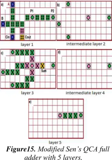
3.6.1. Correcting the Problems of the SEN’S Work and Presents a Validated QCA Full Adder
In this part the problems of the Sen’s work is solved and the new architecture would be named as modified Sen’s QCA full adder. This circuit is shown with five layers in Figure. 15. Two layers and one inverter gate and also some wires have been added to the circuit; furthermore, a valid QCA full adder has been implemented. The modified Sen’s QCA full adder works correctly. This full adder has 54 cells, 0.5 clock cycle delay and 0.05 μm^2 of occupied area.
which are O1=MV3 (A, B, Cin) and
O2=𝑀𝑉3(𝐴, 𝐵, 𝐶𝑖𝑛) .The logical symbol and the cellular structure of this QCA gate are shown in Figure. 16.
Figure14. The Sen’s invalid proposed full adder with 3 layers and 34 cells (Sen
et al., 2013)
Figure15. Modified Sen’s QCA full adder with 5 layers.
The Bandani’s QCA full adder is shown in Figure. 17. This QCA full adder has 48 cells and two clock pulse phases and occupies 0.04 μm^2 of area.
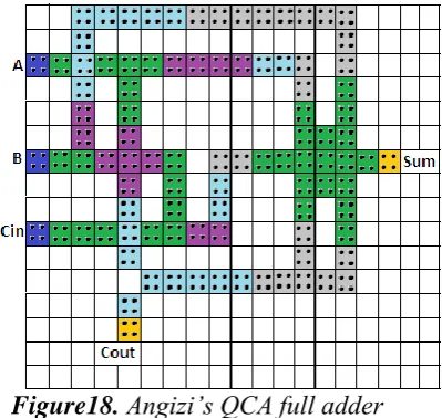
3.8. ANGIZI’S QCA Full Adder
Angizi et al. proposed a new coplanar wire crossing method for designing circuit layout (Angizi et al., 2014). The proposed scheme leads to uniform layout and would
facilitate a defect free fabrication process. The new wire crossing method is integrated into new 2-input and 3-input XOR designs as powerful logic design. The proposed wire crossing and XOR designs are applied to create their full adder. It has 95 cells, 5 clock pulse phases and occupies 0.09 μm^2 of area (see Figure. 18).
(a)
(b)
Figure16. CMVMIN gate (a) cellular structure, (b) logical design
(a)
(b)
Figure17. Bandani’s QCA full adder
Figure18. Angizi’s QCA full adder
More information about other QCA full adders, robustness and crossover connections can be found in references (Safavi and Mosleh, 2013, Hanninen and Takala, 2007, Askari and Taghizadeh, 2011, Haruehanroengra and Wang, 2007, Bhanja et al., 2007, Ganesh, 1824, Ottavi et al., 2006, Zhang et al., 2004, Cho and Swartzlander Jr, 2009, Qanbari and Sabbaghi-Nadooshan, 2013).
4. PROPOSED QCA FULL ADDERS The motivation point for this work is to design an efficient QCA full adder which has a low delay time (less than 4 clock pulse phases), few number of cells (less than 40 cells), low occupied area (less than 0.04 μm^2) with a good robustness against the temperature (more than 5 kelvin's temperature). In the following, two efficient QCA full adders based on the proposed MV32 gate are suggested.
4.1. The First Proposed QCA Full Adder with Single Layer
If the inputs of the MV32 are replaced and configured as represented in Figure. 19(b), then the MV32 produces two outputs including the MV (𝐴 , 𝐵, 𝐶𝑖𝑛 ) and MV(A, B, 𝐶𝑖𝑛 ) functions. These outputs are most important parts of Eq. 10. If these two outputs are combined with Cin input using a 3-input majority gate, then due the Eq. 10, the Sum from the A, B and Cin
inputs will be produced. The OUT1 can be
inverted to generate the Cout because the
Cout is abbreviated from the Eq. 7 and obviously Cout=𝑂𝑈𝑇1 .
(a)
(b)
Figure19. (a) The first configuration for the MV32 gate that produces the truth
table in Table1, (b) The second configuration for MV32 gate for using it in
a QCA full adder
The MV32 is utilized to implement a logical circuit for the proposed QCA full adder. The gate level structure for the proposed QCA full adder can be seen in Figure. 20(a). In this step, the cellular structure for the proposed QCA full adder is going to be implemented. A single-layer cellular structure is shown in Figure. 20(b), but its delay is 4 clock pulse phases (one clock cycle) and it occupies 0.07μm^2 of area and also includes 38 cells. A better QCA full adder using multilayer design would be proposed in the following.
4.2. The Second Proposed QCA Full Adder with Multilayer Structure
carry the Cin, OUT1 and OUT2 signals as pointed in Figure. 20(b).
(a)
(b)
Figure20. (a) The logical circuit for the proposed QCA full adder, (b) The first cellular structure for the proposed QCA
full adder with one layer and 4 phases delay
At the second effort, the 3-input majority gate is placed at the upper layer (the third layer) and sends the Cin, OUT1 and OUT2
signals via the vertical cells to the 3-input majority gate. Therefore, this structure does not need to route the long intermediate wires between the MV32 gate and the 3-input majority gate and consequently one clock phase delay reduces. Note that when a signal propagates from one layer to another layer, it will be inverted. The signals Cin, OUT1
and OUT2 are inverted to 𝐶𝑖𝑛 , 𝑂𝑈𝑇1 and
𝑂𝑈𝑇2 when they propagate from layer 1 to
intermediate layer 2; then they are inverted again when propagate from intermediate layer 2 to layer 3. This full adder has multilayer structure with 3 layers and has three clock pulse phases (0.75 clock cycles) to generate the Sum and Cout
outputs and also includes 31 QCA cells.
As shown in Figure. 21, the multilayer structure of the proposed QCA full adder is different from the former multilayer works because the 3-input majority gate is placed at the third layer of the proposed QCA full adder. But, in former multilayer full adders, the upper layers include just the intermediate wires. In this structure, the
Sum output is generated at the third layer.
(a) (b)
(c)
Figure21. the final design for the proposed QCA full adder with 31 cells, (a) Layer 1,
(b) Intermediate layer 2, (c) Layer 3
Figure.22.Simulation result for the proposed QCA full adder in
QCADesigner2.0.3
5. EXPERIMENTAL RESULTS
results for the proposed full adder are shown; then the results will be compared with the former QCA full adders in some specifications such as robustness, delay, the number of cells and the occupied area. These comparisons will be expanded with some discussions.
5.1. Simulation Results for the Proposed QCA Full Adder
In this section the simulation results for the proposed QCA full adder are shown; then the former QCA full adders would be compared with the proposed QCA full adder; after that the delay, the occupied area, the number of used QCA cells and gates and the robustness of these full adders against the temperature would be focused. The simulation result for the proposed QCA full adder is shown in Figure. 22. As can be seen, the first result for Sum and Cout outputs is generated simultaneously with the falling edge of the clock phase 2 signal. This means the delay time for this full adder is three clock pulse phases (0.75 of a clock period).
5.2. Comparisons and Discussions In this part, the proposed QCA full adder would be estimated and compared in some important properties and some discussions
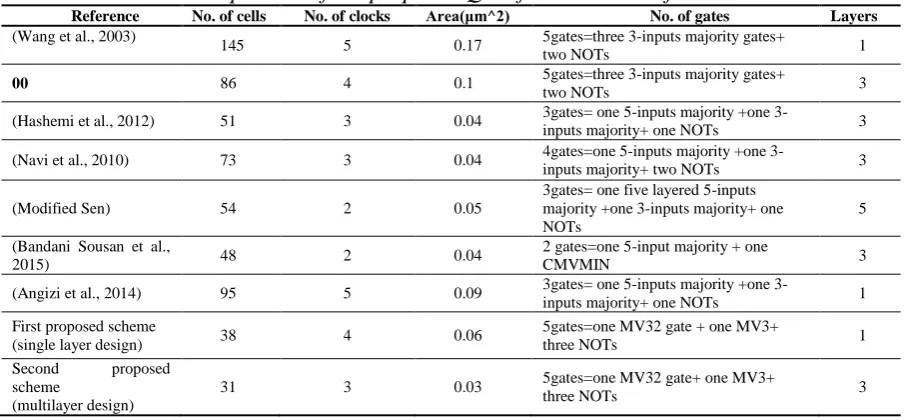
for each comparison will be given. The important specifications for the QCA full adders are shown in Table 2.
Generally, two types of QCA full adders can be found in the Table 2; The first type of full adders such as the Angizi’s, the modified Sen’s, the Hashemi’s, the Bandani’s and the Navi’s QCA full adders use the 5-input majority gate to produce the Sum output. The 5-input majority gate is the main building block for these designs. The second type of full adders such as the Cho’s, the Wang-Walus and the proposed QCA full adders use the same algebra equations for generating the Sum output. These full adders in this type have five QCA gates and use the 3-input majority gates as the main building block. Clearly, the proposed QCA full adder employs the MV32 as the main building block and can take place in a new type.
The proposed QCA full adder with 31 cells is so better than other QCA full adders in the case of number of used cells; this efficiency is because of using the proposed MV32 and multilayer structure. The Wang-Walus work is not acceptable in number of used cells feature because its coplanar crossover connections consume many QCA cells.
Table2. Comparison of the proposed QCA full adder with former works
Reference No. of cells No. of clocks Area(μm^2) No. of gates Layers (Wang et al., 2003)
145 5 0.17 5gates=three 3-inputs majority gates+ two NOTs 1
00 86 4 0.1 5gates=three 3-inputs majority gates+
two NOTs 3
(Hashemi et al., 2012) 51 3 0.04 3gates= one 5-inputs majority +one
3-inputs majority+ one NOTs 3
(Navi et al., 2010) 73 3 0.04 4gates=one 5-inputs majority +one 3-inputs majority+ two NOTs 3
(Modified Sen) 54 2 0.05
3gates= one five layered 5-inputs majority +one 3-inputs majority+ one NOTs
5
(Bandani Sousan et al.,
2015) 48 2 0.04
2 gates=one 5-input majority + one
CMVMIN 3
(Angizi et al., 2014) 95 5 0.09 3gates= one 5-inputs majority +one
3-inputs majority+ one NOTs 1 First proposed scheme
(single layer design) 38 4 0.06
5gates=one MV32 gate + one MV3+
three NOTs 1
Second proposed scheme
(multilayer design)
31 3 0.03 5gates=one MV32 gate+ one MV3+
Among the first type of the QCA full adders which use the 5-input majority gate as the main building block, the Bandani’s QCA full adder is very good and the Hashemi’s full adder with 51 cells is good in this class. The modified QCA full adder with 54 cells is a suitable full adder too. The modified Sen’s QCA adder with two clock pulse phases is an acceptable QCA full adder in delay factor because this full adder has two levels of logic and these two levels of gate can be placed in two clock zones. The Bandani’s work with 2 clock pulse phases is a high speed full adder. The Hashemi’s, the Navi’s, the Cho’s and the proposed QCA full adders are similar in delay time (3 clock pulse phases). Clearly, the occupied area property depends on other features such as the number of used cells, the techniques for building the cellular structure for the full adder such as multilayer and coplanar crossover connections and also using the novel structures such as the MV32 and the 5-input majority gate. As can be seen in Table 2, the proposed QCA full adder is an appropriate QCA full adder in this factor. The modified Sen's, the Hashemi’s, the Navi’s and the Cho’s QCA full adders are in the next places. The single-layer structures such as the Wang-Walus work are not so good in this property.
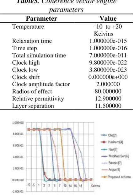
Now, the QCA full adders are being compared on robustness against the temperature feature. Recent nanometer sized devices such as the QCA devices are sensitive to temperature. As can be seen in Figure. 23, the proposed full adder, the Cho’s full adder and the modified Sen’s full adder are robust and they are approximately similar in this feature. The Bandani’s QCA full adder is more robust than the modified Sen’s full adder. Other QCA full adders such as the Navi’s and the Hashemi’s works are limited to 1 or 2 kelvin temperature and after this threshold temperature, they cannot generate a correct output.
We obtained these results using the QCADesigner 2.0.3 software and the
coherence vector options for these simulations are shown in Table 3. Some former works and the proposed work have been simulated; in this process the temperature option has been changed from -10 kelvins to +20 kelvins degree for each QCA full adder; after that generation and the amplitude of the Sum signal have been tested. The Cout signal is produced for all QCA full adders by using a 3-input majority gate and similar results are obtained for it. Therefore, the results have not been revealed for the Cout signal.
Table3. Coherence vector engine parameters
Parameter Value
Temperature -10 to +20
Kelvins Relaxation time 1.000000e-015
Time step 1.000000e-016
Total simulation time 7.000000e-011
Clock high 9.800000e-022
Clock low 3.800000e-023
Clock shift 0.000000e+000
Clock amplitude factor 2.000000 Radios of effect 80.000000 Relative permittivity 12.900000 Layer separation 11.500000
Figure23. Comparing the QCA full adders on robustness against the temperature
factor for the Sum signal
6. CONCLUSION
QCA full adder. A single-layer implementation of the proposed QCA full adder include 38 cells, 4 phases delay and 0.06 μm^2 of the occupied area. Moreover, its multilayer implementation consists of 31 cells, 3 clock phases and the 0.03 μm^2 of occupied area. The simulation results show that the proposed QCA full adder is so better than other QCA full adders in the case of number of used cells and occupied area features. Despite of its low cost and low occupied area, the proposed QCA full
adder has a high robustness against the temperature. The proposed QCA full adder can be changed to obtain a more robust or faster QCA full adder by increasing the number of cells or reducing the latency of the MV32 gate. The MV32 structure with a systematic method is denoted and other useful structures can be found using this method and then these structures can be used to implement efficient arithmetic and logic circuits.
REFERENCES
1. ANGIZI, S., ALKALDY, E., BAGHERZADEH, N. & NAVI, K. (2014) Novel robust single layer wire crossing approach for exclusive or sum of products logic design with quantum-dot cellular automata. Journal of Low Power Electronics, 10, 259-271.
2. ASKARI, M. & TAGHIZADEH, M. (2011) Logic circuit design in nano-scale using quantum-dot cellular automata. European Journal of Scientific Research, 48, 516-526.
3. AZGHADI, M. R., KAVEHEI, O. & NAVI, K. (2007) A novel design for quantum-dot cellular automata cells and full adders. Journal of Applied Sciences, 7, 3460-3468.
4. BANDANI SOUSAN, H.-A., MOSLEH, M. & SETAYESHI, S. (2015) Designing and Implementing a Fast and Robust Full-Adder in Quantum-Dot Cellular Automata (QCA) Technology. Journal of Advances in Computer Research, 6, 27-45.
5. BHANJA, S., OTTAVI, M., LOMBARDI, F. & PONTARELLI, S. (2007) QCA circuits for robust coplanar crossing. Journal of Electronic Testing, 23, 193-210.
6. CHO, H. & SWARTZLANDER JR, E. E. (2009) Adder and multiplier design in quantum-dot cellular automata. IEEE Transactions onComputers, 58, 721-727.
7. GANESH, E. (1824) Implementation and simulation of arithmetic logic unit, shifter and multiplier in Quantum cellular automata technology. International Journal on Computer Science and Engineering, 2, 2010.
8. HANNINEN, I. & TAKALA, J. (2007) Robust adders based on quantum-dot cellular automata. IEEE International Conf. on Application-specific Systems, Architectures and Processors ,391-396.
9. HARUEHANROENGRA, S. & WANG, W. (2007) Efficient design of QCA adder structures. Solid State Phenomena,121,553-556.
10. HASHEMI, S., TEHRANI, M. & NAVI, K. (2012) An efficient quantum-dot cellular automata full-adder. Scientific Research and Essays, 7, 177-189.
11. NAVI, K., FARAZKISH, R., SAYEDSALEHI, S. & AZGHADI, M. R. (2010) A new quantum-dot cellular automata full-adder. Microelectronics Journal, 41, 820-826.
12. OTTAVI, M., PONTARELLI, S., DEBENEDICTIS, E. P., SALSANO, A., FROST-MURPHY, S., KOGGE, P. M. & LOMBARDI, F. (2006) Partially reversible pipelined QCA circuits: combining low power with high throughput. IEEE Transactions on Nanotechnology,, 10, 1383-1393.
13. QANBARI, M. & SABBAGHI-NADOOSHAN, R. (2013) Two Novel Quantum-Dot Cellular Automata Full Adders. Journal of Engineering, 2013, 1-6.
14. SAFAVI, A. & MOSLEH, M. (2013) An Overview of Full Adders in QCA Technology. International Journal Of Computer Science and Engineering, 1, 12-35.
15. SEN, B., RAJORIA, A. & SIKDAR, B. K. (2013) Design of efficient full adder in quantum-dot cellular automata. The Scientific World Journal, 2013, 1-10.
16. WANG, W., WALUS, K. & JULLIEN, G. A. (2003) Quantum-dot cellular automata adders. Third IEEE Conference on Nanotechnology,1,461-464.