Preparation, Characterization And Optical
Properties Of Copper Oxide Thin Films
Zainab K. Lateef , Muneer H. Alzubaidy , Najwa J. Jubier
Department of Physics, Collage of Science, University of Wasit, Iraq Corresponding author, E-mail:ahmed_naji_abd@yahoo.com
Abstract—Copper Oxide was deposited on glass slides as a substrate by the drop casting method at room temperature with a thickness of films (235and400)nm. The films were thermal treated at (500ºC) for one hour. The structural properties were diagnosed by using X-ray diffraction (XRD), the pattern of diffraction showing that the deposited films are polycrystalline in nature, the inter-planar spacing (d) and the grain size were calculated. The obtained results showed that the grain size increased with the increasing temperature. An atomic force microscopy technique (AFM) was used to measure the roughness of the prepared samples. The optical properties have been studied by using (UV-VIS) spectroscopy and Tauce's Method. The results show that the energy gap of 400 nm thickness of CuO thin film decreases when the films thermal treated at 500ºC from (2 to 1.68) eV, also increases with the increase of thickness, also the transmittance decreased after thermal treatment. The samples tested by optical microscopy to choose the best sample without any cracks.
Keywords—Copper Oxide , Tauce's Method , thin film , XRD
1. Introduction
- Copper oxide is an important semiconductor material with superconductivity properties, having immense application in sensors, field emission and photonic devices [1,2].It can be obtained from metallic copper oxidation and it is a p- type, that’s mean the most carriers charge is holes [3]. There are two types of copper oxide, the first is a tenorite or cupric oxide, it is considered a stable type of copper It has polycrystalline structure and crystalline monolithic installation [4]. It is characterized by being the dark brown color and has a non-toxic and odorless nature as well as the possibility of availability and ease of production at low cost [5,6]. It has an Energy gap between the nearbyvisible and infrared spectrum with values (1.21-1.51eV) [7]. The Second type of copper oxide is cuprite or cuprous oxide [8], it is less stable than the first type and is a crystalline powder brown depending on the method of preparation and the size of the crystal. It is characterized by being a cubic shape and its energy gap values (2.1-2.6eV).It is used in photovoltaic complex requiring high efficiency [5, 8], good range of stability and high absorption in the visible wavelength range.
2. Deposition of Thin Films by Drop
Casting Method
www.jmess.org
JMESSP13420392 2013
phase crystalline . The average grain size and roughness of CuO were investigated by using AFM (AA3000 scanning probe Microscope ). The sample was examined with the optical microscope (Nickon Eclipse-ME600) to select the best samples without sharp edge and cracks.
Figure (1): Image of CuO Nanoparticles Colloidal dissolved in PVP.
The inter planer distance (d) for different planes were measured by Bragg's law [9,10]:
𝟐𝒅 𝒔𝒊𝒏 𝜽 = 𝒏𝝀 (𝟏)
Where: (𝒏) is the reflection order, ( 𝒅) estimated
from the relation (2)[11]:
β)+(2hlcos 2 sin 2 /c 2 )+(l 2 /b 2 β)+(k 2 sin 2 /a 2 )=(h 2 (1/d ) 2 ( ) β 2 β/acsin
The grain size dimension diffraction could be calculated from Debye-Scherer formula (XRD) as in equation (3)[12]:
𝑫 = 𝑲𝝀 𝜷 𝐜𝐨𝐬 𝜽 (𝟑)⁄
Where: (𝑲) is the shape factor and equal (0.94), ( 𝜽) is the diffraction angle (λ) is the x-ray wavelength and (𝜷) is the line broadening.
For optical parameters the Transmittance denoted (T), (α ) Absorption coefficient, (t) thickness of films, (Eg) Energy gap, E(h𝝂) Photon energy (eV) The photon energy (hν) can be calculated using equation(4)[13] :
𝑬(𝒆𝑽) = 𝟏𝟐𝟒𝟎 𝝀(𝒏𝒎)⁄ (𝟒 )
The value of absorption coefficient (α) was determined by the equation (5) [13] :
α =2.303A/t (5)
3. Result and Discussion
3.1Structural Properties Measurements:
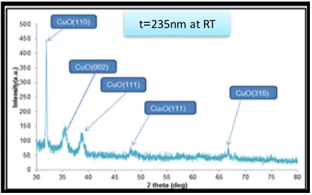
X-ray diffraction (XRD) studied by using X-ray diffractometer (XRD-6000, shimadzu), analysis of diffraction spectra indicates the peak position for CuO films of 235nm thickness. As evidenced from Fig.(2) the relationship between the intensity of x-rays and Bragg's angle for the copper oxide film deposited on the glass slide that there are narrow distinct peaks corresponding to diffraction angle (33º,35º,38º,67º) and diffraction from planes of the (110), (002), (111) , (310) for CuO and (111) for Cu2O at diffraction angle (47º) reported by refs [14]. the lattice parameters for
monoclinic CuO
a=4.688(4)Aº,b=3.4229(2)Aº,c=5.1319(3)Aº, it is represents the copper oxide pattern according to the international standard card (00-035-1091).
Figure (2): X-ray pattern of copper oxide thin films prepared on glass substrate with thickness (235nm) as deposited.
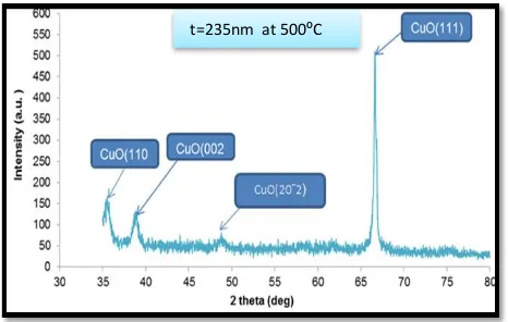
It is clear from Fig.(3) when the film treated thermally at high temperature 500ºC the Cu2O bond is broken and another phase appears (202 ̅ )that’s mean that the film becomes more crystalline and the phase (110) change and disintegration because of the weak bond between the grains. The grain size decreases, crystallization increases and Miller indices change due to change of phase from the cubic to monoclinic after applying high temperature , this result according to the international standard card (00-044-0706). From the results obtained from
235nm at RT
=
the patterns of diffraction indicate that the deposited films are polycrystalline in nature[15].
Figure (3): X-ray pattern of copper oxide thin films prepared on glass substrate with thickness (235nm) after
thermal treatment.
The morphology, roughness and grain size were investigated as shown in Fig. (4) by using atomic force microscopy (AFM). It was found that the roughness of CuO thin film of thickness (235nm) is (0.589nm), the average grain size is (70.36nm) and the root means square is (0.746).
Figure (4): AFM Images for copper oxide thin film of thickness(235nm) .
3.2 Optical measurements
From the results obtained by using (UV-VIS) spectroscope, the transmittance has been studied. Fig.(5) shows the relationship between the transmittance spectrum and the wavelength for the CuO thin films deposited on glass substrate , it is clear from figure that the transmittance was increasing with the increased of wavelength and decreasing after thermal treatment at 500ºC temperature while, when the thickness of films was increased the transmittance was decreasing .
www.jmess.org
JMESSP13420392 2015
Figure (5): the relation between the transmittance and the wavelength before and after thermal treatment.
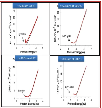
The energy gap for the allowed direct transmittance is calculated by plotting the relationship between (𝛼ℎ𝜈)² and the photon energy; for thickness (235nm) it is increased after thermal treatment because that the high temperature increases the crystalline size of the thin film and decreases crystalline defects , resulting in a decrease in the levels of the defect within the energy gap, so that the energy gap increased, this can be attributed to the change of lattice constant or to the change of thin film composition from cubic phase to monoclinic phase [14] . For the thickness (400nm) we notice that the energy gap decreased and this can be explained by the increase in thickness led to a clear increase in the number of photon collisions with the material and this will lead to an increase in the number of electrons and holes leading to a decrease in the energy gap, the result agrees with the results of refs [15]. The value and type of energy gap depend on the material, its nature and
the impurities in its composition [7]. Fig. (6) Shows this relationship.
Figure(6):The direct allowed energy gap for CuO thin films of thickness (235 , 400)nm at room temperature and 500°C from the relationship between (𝜶𝒉𝝂)² versus photon energy gap.
Figure (7): Image of optical microscope for copper thin film with thickness 235nm (a) at roo
t=235nm at RT t=235nm at 500°C
www.jmess.org
JMESSP13420392 2017
Conclusion:
Copper oxide thin films at thickness
(235,400) nm deposited by the drop
casting method. In our research we studied
in detail the influence of thickness and
thermal treatment on the structural and
optical
properties.
XRD
diffraction
patterns showed that the thin film
polycrystalline, and has monoclinic crystal
structure, also we noticed tetragonal and
cubic phases, it is clear that the thermal
treatment at temperature (500ºC) caused
an increase in grain size, and the film
become more crystalline, the tetragonal
and cubic phases converted to monoclinic.
The morphology , grain size and
Roughness
obtained
from
AFM
microscopy, the results showed that the
CuO thin film have spherical shaped with
good homogeneous. The energy gap
values increase with the thickness, and
decrease after thermal treatment at
(500ºC).Copper
oxide
have
high
transmittance in the near infrared region.
The image of optical microscope revealed
the cracks and needle grains getting
agglomerated.
References:
[1]. D. A Gerdeman and N.L. Hecht" Arc Plasma Technology in materials science"spring erverlage, New York, (1972).
[2].A. k. Abass, Sol." Energy Mater" Vol.17, PP.375-378, (1988).
[3]. A. E. Rakhshani, "Solid State Electron"Vol.7, PP.29, (1986).
[4]. J. B. Forsyth, S .Hull, "The effect of hydrostatic Pressure on the ambient temperature Structure of
CuO" J. Phys.condens. Matters, pp.5257-5261, (1991).
[5]. H. M. Xiao, S.Y. Fu, L.P. Zhu, Y. Q. Li, G. Yang,
Eur." J.I norg. Chem.", Vol.14, (2007).
[6]. N. N Green wood and A. Earnsham, "In
Chemistry of the elements." 2nd Ed., Buttworth , UK, (1997).
[7]. Necmi serin and Tulay serin" Annealing effects
on the properties of copper oxide thin films prepared by Chemical deposition" Semicondsci. Technol, Vol.20, PP.398-401, (2005).
[8]. T. Kaelsson A.Roos,"Solar energy
material"Vo.10, PP.105-119, (1984).
[9]. B. D. Cullity. "Elements of X-Ray Diffraction "
Addision -wesley Reading, MA, (1970).
[10]. A. J. C. Wilson, "X-Ray Optics, "Lonon: Methnen &Coltd New York: John Wiely & Sons Inc, PP.1-5, (1962(.
[11]. W. d. Callister, "Materials Science and Engineering-An Introuction ", John Wiely and Sons, New York, (1997).
[12]. Hayder M, Shatha S, Ashwaq A,and Elham H,"The Effect of Annealing on the Structural and optical Properties of Copper Oxide Thin Films Prepared by SILARMethode." J. Baghdad for Sci.",Vol.11 (2014).
[13]. Samir H. Awad and Riyam I. Jadaan,"Study The Optical Properties of Copper Oxide Thin Film Deposited by Cold Spray."Al-Qadisiya Journal For Engineering Sciences", Vol.6, No.4,( 2013).
[14]. I. V. Bodnar, V. P. Gremenok, E. P. Zaretskaga and I-V. victorov, Thin Solid films 207 (1992) p, 54.
[15]. Rawaa A. Faris. "Synthesis,
Characterization, and optical properties of copper oxide thin films obtained by spray pyrolysis." ,Iraqi Journal of Physics", Vol. 11, No.22, PP.64-71, (2013).