Journal of Solar Energy Research Vol 4 No 4 Autumn (2019) 287-299
287 1. ntroduction
Photovoltaic (PV) power generation has obtained importance as a renewable energy source as of its several deserves such as clarity of allocation, absence of noise, extensive life, absence of pollution, less time for installation, high movability and portability of parts, and the output power capability to match peak load requirements [1]. However, PV generation systems have faults including lowering in the conversion efficiency and dependence on climate conditions [2]. PV arrays have been take care of for a variety of applications, such as battery charging systems, solar-powered water-pumping
systems, solar hybrid conveyances, and satellite power systems [1,3]. Several countries, such as China, Finland, New Zealand, Canada, South Korea, and Spain are allocating funds to support renewable energy-based projects [4–9]. There have been numerous publications related to the scope of renewable energy in various countries. For example, Yushchenko et al. [10] analyzed land suitability factors for large-scale grid-connected concentrated solar power plants and PV systems as well as off-grid PV systems in countryside areas of West Africa. Studies on the status of current renewable energy sources
Click here, type the title of your paper, Capitalize first letter of each words
First Author
a, Second Author
b,*aFirst affiliation, Address, City and Postcode, Country
bSecond affiliation, Address, City and Postcode, Country
Journal of Solar Energy Research (JSER)
Journal homepage: jser.ut.ac.ir
ARTICLE INFO :
Received in revised form: Accepted:
Available online:
Keywords:
Type 3-6 keywords here,
separated by semicolons ;
Boost converter topologies, hybrid boost and new topologies of voltage
multiplier in photovoltaic systems
Mohamadreza samadi
a*, Seyed mehdi rakhtala
b, Morteza ahmadian
ca* Faculty of Electrical and Computer Engineering, Mazandaran Regional Electric Company, Sari, Iran
b Assistant Prof., Faculty of Electrical Engineering, Golestan University, Gorgan, Iran
c Electrical Engineering, Power Distribution Company of Mazandaran, Sari, Iran
A B S T R A C T
Renewable energy generation has experienced lot growth in the last not many years, with close to several billion dollars financing in 2017. Selection of an appropriate converter is one of the challenges since it has an impact on the behavior of the PV (photovoltaic) system. In recent years, many converters have been reported in the literature.
This paper presents a review of non-isolated C-DC converters of voltage enhancers. Relevant review details are presented about the topologies of converters, including boost, hybrid boost, three-level boost, multi-level boost, and three-level hybrid converters that are most commonly used in photovoltaic systems. In the end, there are also several voltage level enhancers that can replace the converters provided in photovoltaic systems. Finally, a comparison is made between the converters in terms of the number of elements used in the circuit and the complexity of controlling the switches in the converters with their advantages and disadvantages being presented in a table. Since the use of multi-level boost converters reduces the switch voltage stress, weight, and cost compared to the conventional mode and as they are also better at higher powers, they have been used significantly in different systems.
© 2019 Published by University of Tehran Press. All rights reserved.
ARTICLE INFO
Received:
Received in revised form: Accepted:
Available online:
in Mexico have been done by Alemán-Nava et al. [11]. In the Middle East, the problems and disputes in the field of renewable energy were analyzed for Yemen by Rawea and Urooj [12]. The main challenges are related to financial, market, technical, social, and institutional barriers. The author suggested recommendations such as research and development, creation of a schedule for the production of renewable energy, improvement of market policies and development of distributed generation. Honrubia et al. [13] evaluated the economic details of PV power plants in Europe. Photovoltaic power differs with insolation, temperature, and load features [14,15] and it is straightly proportional to irradiance and inversely equivalent to temperature. The circuit-based model of a solar cell as shown in Fig. 1 consists of a current source connected in parallel with a diode. The current’s source illustrates photon-generated currents (Iph). The resistance Rs
represents the losses due to the contacts and connections. The leakage currents in the diode are represented by parallel resistance Rp [16]. Parameters like the
short-circuit current (Isc) and open-short-circuit voltage (Voc) are used to examine the characteristics of a Photovoltaic cell. The Isc is the maximum value of the current produced by a
cell, and is sensitive to irradiance. The Voc is the
maximum value of voltage obtained from a solar cell at zero current. The I–V characteristics of a solar cell are shown in Fig. 2. There is no intersection between the voltage characteristics of the PV generator and DC bus since the DC bus voltage is far higher than Voc [2,29].
In PV systems, high voltage is favorable, like in uninterruptible power supplies (UPS) and micro PV inverters [17-19]. For such approaches, little input voltage from PV the source should be stepped-up. For example, in micro PV inverters, interfacing PV panel with a 230 VRMS
grid requires the low PV voltage (typical around 30 VDC)
to be stepped up to around 375-400 VDC[13, 20-22]. For such applications, the voltage boosting required is too big to be accessible appling conventional fundamental boost DC-DC converter topology; therefore there remains a urgency for modified topologies offering a high voltage gain. DC-DC converters are commonly been categorized into isolated and non-isolated topologies [23-28].
contrary to many various topologies, the conventional boost converter yet enjoys remarkable degree of amicability due to the following advantages: little number of components which explicate into system cost decrease; non-pulsating input current (if the converter acts in CCM), and ordinary drive circuit. For this reason, the main emphasis of the paper is on non- isolated DC-DC converters from boost and hybrid boost converters as well as some converters for photovoltaic systems.
The main objective of the paper is introducing:
1.Conventional boost converters and hybrid boost converters
2.Three-level boost converter and three-level hybrid boost converter.
3.A Multi-level boost converter
4.Voltage multiplier converters for future work on its application in photovoltaic systems
The remainder of the paper is organized as follows. The second section deals with introducing isolated and
non-isolated DC-DC converters. Section 3 introduces conventional boost converter and hybrid boost converter, three-level boost converter and three-level hybrid boost converter, multi-level boost converter and some proposed voltage multipliers and, finally, discusses the comparison between existing converters.
Figure 1: Equivalent model of the PV cell[29].
Fig. 2. I-V Characteristics of solar cell with load line.
2. Isolated and non-isolated DC–DC converts
Figure 3 presents only the chief isolated and non-isolated converters [23-28].
The DC-DC converters are generally categorized into isolated and non-isolated converters. The input and output voltage are separated from each other in isolated convertors and there is greater protection between them, while the input and output voltages are not separated in non-isolated convertors and they are related to each other, which is called non-isolated.
DC-DC converters
Isolated Non-Isolated
Cuk converter SEPIC
Boost converter
Buck-Boost converter
Non-transformer Multi level
Non-transformer
hybrid converter
New Non-Transformer Converters
Flyback converter
Forward converter
Push–pull converter
Full-bridge converter
Half-bridge converter
transformers Multi level
transforme rs hybrid converter
New Transformers
Converters
Fig. 3. Isolated and non-isolated DC–DC converts
Iph D Rp
Rs
+
Journal of Solar Energy Research Vol 4 No 4 Autumn (2019) 287-299
289 3. Types of boost converter topologies
3.1. Boost converters
A boost converter is a DC-DC converter that is capable to produce an output voltage greater than the input voltage. Since the output voltage of a boost converter is greater than the input voltage, it is also known as step-up converter [30-34]. According to the law of conservation of energy, the input power must be equal to the output power. Since the output voltage of a boost converter is greater than its input voltage, the output current will be lower than the input current. The circuit topology of a conventional boost converter is shown in Fig. 4.
When the switch is made ON, one direction of the inductor suits linked to the source of energy. The current via the inductor ascents from the least level to its most level during this course. The output voltage appears in the cathode while zero voltage appears in the anode of the diode hence it is reverse biased and OFF. So, the load is isolated from the source pending the ON period, and in turn the load current is retained continuous by the output hand capacitor. When the switch is turned OFF, the plural of the voltage of the inductor and source voltage becomes visible on the switch and in the anode of the diode that is greater than the output voltage. So, the diode obtains forward biased and onsets the conduction current. Pending this period, the inductor current falls from the topmost level to least level where all energy stored in it along with the source voltage is rendered to the load and output capacitor. The output current is always continuous in the boost converter, while the input current can be continuous or discontinuous. This converter has been widely used in photovoltaic systems [35-38].
PV panel
L
C
R
+
_
V
o+
_
V
i+ _
v
LS
D
Fig. 4. DC-DC Boost converter[24].
3.2. Hybrid boosting converters
A hybrid boosting converter or (HBC) using bipolar voltage multiplier or (BVM) is shown in Fig. 5. The characteristics of interleaving are inherited to this converter which reduces the voltage on the output filter capacitor while enhancing the utilization rate of the components as the voltage gain is higher during a shorter duty cycle. Topologies in [39,40] have employed an interleaving method for ripple decrease and power increment; although, these topologies require rather components. This converter represents minor ripples while maintaining high voltage gain with only one single
inductor and single switch. A higher gain was archived in topologies in [41-46], but they implemented two inductors and two switches. The HBC topology has advantages including low-cost design and the potential to be employed in high power applications. As a disadvantage to applications where common ground is required, this topology has different grounds for the source and load. Moreover, due to this problem, audible noise may be experienced, which may necessitate a fast control loop and an input filter.
Vg
C
a2C
a1C
b1C
b2D
a1D
a2D
b1D
b2S
L
V
o +_
Fig. 5. Hybrid Boosting Converter [47].
3.3 Three-level boost type converter (TLBC)
As shown in Fig. 6, the switching signal G1 is obtained
from the comparison of the control signal vcont1 with the
triangular signal vtri1. Due to the low output voltage ripple,
VO is assumed constant. Therefore, the sum of two
capacitor voltages will be fixed vC1 + vC2 = VO.
In addition, the other switching signal G2 is obtained by
comparing the control signal vcont2 with the triangular
signal vtri2, where there is a 180º phase differencebetween
two triangular signals.
Due to the input inductor L and two diodes D1 and D2 in
the TLBC, both switches can be turned on at the same time. Therefore, there are four possible switching states as plotted in Fig. 7.
In Table 1, the states are described as follows: State (a) : T1=ON and T2=ON then VPV=VL.
State (b) : T1=ON and T2=OFF then VL=Vpv -VC2 then C2
capacitor is charged.
State (c) : T1=OFF and T2=ON then VL=Vpv -VC1 then C1
capacitor is charged.
State (d) : T1=OFF and T2=OFF then VL=Vpv -VC1-VC2.
All of the capacitor currents in various switching states are tabulated in Table 1.
In case 1 < vcont1 + vcont2 <2, vcont1=0 and vcont2=0 do not
occur at the same time. Therefore, State 4 in Figure 4 does not develop.
In case 0 < vcont1 + vcont2 <1, vcont1=1 and vcont2=1 do not
Table 1: Capacitor currents in each state
PV
panel
L
D
1D
2C
1C
2R
T
1T
2i
L,i
PVi
Oi
C1i
C2+
_
+
_
v
PVThree-Level Boost Converter
+ +
_ _
v
tri1v
tri2Comp
v
cont1+
_
+
_
v
C1v
C2v
cont2 0 0 1 1v
tri1v
tri2T1 T2
i
pvV
pv MPPT+ + _ _
V
C1V
C2 _K
pFig 6. Three level boost converter[49].
PV panel
L
C
1C
2R
T
1T
2i
L,i
PVi
Oi
C1i
C2 + _ Vo + _v
PV + _ + _v
C1v
C2 + _v
Lon
on
(a) PV panelL
D
2C
1C
2R
T
1i
L,i
PVi
Oi
C1i
C2 + _V
o + _v
PV + _ + _v
C1v
C2+
v
_L
on
(b) PV panelD
1C
1C
2R
T
2i
L,i
PVi
OiC1 iC2 + _
V
o + _v
PV + _ + _v
C1v
C2+
v
_L
on
L
(c) PV panelL
D
1D
2C
1C
2R
i
L,i
PVi
OiC1 iC2 + _
V
o + _v
PV + _ + _v
C1v
C2 + _v
L (d)Fig. 7. Possible switching states in three-level boost-type converter: (a) state 1; (b) state 2; (c) state 3; (d) state
4[49]. Switchin g States of TLBC Capacitor Output current State 1
State 2 State 3 State 4
1<vcont1 +vcont2< 2
iC1 −iO
< (0)
−iO <
(0)
iL−iO
> (0)
iC2 −iO
< (0) iL−iO
> (0)
−iO <
(0)
0<vcont1 +vcont2< 1
iC1 −iO <
(0)
iL−iO
> (0)
iL−iO
> (0)
iC2 iL−iO
> (0)
−iO <
(0)
iL−iO
Journal of Solar Energy Research Vol 4 No 4 Autumn (2019) 287-299
291
As shown in Fig. 6, the current and PV voltage are sensed and introduced into the MPPT control block. This block generates the output signal vcont1. The existing signal is
compared with the triangular signal vtri1 with zero-phase
angle and can create signal G1 for switch SW1. Then,
voltage capacitors C1 and C2 are sensed and compared with
one another to obtain an unbalanced voltage. This signal is then introduced into the proportional control to make the errors zero. The resulting signal from the controller output is added to signal vcont1. The obtained signal is then
compared with signal vtri2 (there is 180ᵒ phase difference
between vtri2 and vtri1). Next, the obtained signal G2 enters
the second switch. In this way, two rates of D1 and D2will
be created with half of the period of the phase difference, where, three-level voltage is obtained in the output converter. This not only increases the input voltage, but also reduces the switch voltage stress. It can also lower the filter size due to increased frequency [48-51].
3.4. Hybrid boost three-level DC-DC converters The single-phase diode-clamped three-level inverter is shown in Fig. 8(a), where there are four switches Qa1 − Qa4 with corresponding antiparallel diodes Da1 − Da4 . Leaning on this topology, two three-level DC-DC converters (buck and boost converters) are deduced, as shown in Fig. 8(b) and (c). Note that there are still two other boost three level converters shown in Fig. 9 [18], which can also be deduced from the inverter in Fig. 8(a). However, these two boost three level converters cannot operate individually, due to the unbalanced capacitor voltages across (C11, C12 ) or (C21, C22 ). For both
improving the dc-bus voltage and power level of PV generation systems and for obtaining narrower pulse voltages from the difference between wider ones through the idea based on the topology of a single-phase diode-clamped inverter with two three-level legs , a new hybrid boost three- level converter can be combined naturally by the two boost three-level Converters I and II in Fig. 9. Vin1,
Vin2, and Lf 1, Lf 2 represent the input dc voltages and
filtering inductors of Converters I and II, respectively. Then, the input power level of the hybrid converter can be improved by two inputs of two series converters called
Vin1 + Vin2 . Also, the output power level of the hybrid
converter can also be enhanced by the parallel connected outputs of Converters I and II called (i1 + i2 ) as displayed
in Fig. 9. Accordingly, the process of synthesizing the hybrid converter by the mode of inputs in series and outputs in parallel is depicted in Fig. 10. The input node c
is cut off from node g1 in Converter I, which is abbreviated as “Cut I.” In addition, the other input node d
is also cut off from node p2 in Converter II, abbreviated as
“Cut II.” Then, the two input nodes c and d can be connected in series, i.e. both of the input dc voltage supplies Vin1 and Vin2 are in series. On the other hand, the
output structures of Converters I and II are identical, nodes
p1 and p2, as well as g1 and g2 can be connected in parallel
leading to the “paralleled output +” and “paralleled output –” for the hybrid converter as shown in Fig. 10. The synthesized hybrid boost three-level converter is shown in Fig. 11, where the equivalent input dc voltage Vin and
inductor Lf can be obtained linearly due to the input sides of Converters I and II in series.
In addition, the parallel-connected capacitors (C11, C12 )
and (C21, C22 ) as shown in Fig. 10, can be equivalent to Cf 1 and Cf 2 in Fig. 11, as well as the parallel-connected load
resistors R1 and R2 which are equivalent to RL. However, the neutral points n1 and n2 in Fig. 10 have to be connected
to each other, leading to the neutral point n which may keep the blocking voltages across power switches as the corresponding capacitors’ voltages in Fig. 11. So, the proposed hybrid converter, combined by Converters I and II in Fig. 9, contain Half-Bridges I and II, as shown in Fig. 11.
The significant point on this hybrid converter is that one inductor, two capacitors in series, and those power switches and diodes, which are simple to be united, are pursue to instate the topology with a transformer-less great voltage gain.
So, the proposed converter can both act with a high voltage gain and fetch the duty cycles of power switches near to 0.5.
Also, the voltages through the capacitors in series are well balanced in both stable and dynamic states, As the blocking voltages of the power switches are half of the output dc voltage. Finally, a 1-kW archetype is set up in our laboratory, where the measured maximum revenue of the proposed converter is about 93.1%.
The three-level hybrid boost converter conversion function is also described further:
d1 and d2 are the duty cycles of Q1 and Q2 , respectively.
Then, all the duty cycles of power switches can be described as follows with the modulation indices ma and
mb:
a b
m
d
d
m
d
d
3 2
4
1
1
(1)Also, d3 and d4 are the duty cycles of Q3 and Q4,
respectively. Then, the voltage gain M of the hybrid converter is written as follows by:
(2)
(a)
b ain o
m m d d V
V M
1
1 1
2 1
Lf Vin
C1
C2
n
g
Dc1
Dc2
Qa1
Qa2
Qa3
Qa4
Da1
Da2
Da3
Da4
x
y
iL
p
+
-+
-i
LL
fC
1C
2Q
a1Q
a4D
a2D
a3p x
n a
g y
(b)
(c)
Fig. 8. Single-phase diode-clamped three-level inverter and two classical three-level dc–dc converters[52].
(a)
(b)
Fig. 9. Two deduced boost three-level dc–dc converters[52].
Lf2
Dc3
Dc4
Qa1
Qa2
Da4
Da3
iL2 Vo2
b
g2 n2 p2
C21
C22
R2
Vin2 i2
d
Lf1
c
C11
C12
a p1 i1
Dc1
Dc2
R1 Vo1 n1
g1
Vin1 iL1
Qa3
Qa4
Da1
Da2
Cut I
Cut II Paralleled output +
Paralleled output - Converter II Converter I
Fig. 10. Synthesized process of the hybrid boost three-level dc–dc converter by the mode of inputs in series and
outputs in parallel[52].
Fig. 11. Proposed hybrid boost three-level dc–dc converter[52].
3.5. Analysis of the new Converter
The new converter with two switches is shown in Fig. 12, where Vin is the input voltage and the resistor Ro
represents the load. Each of the two phases of the converter is composed of one switched inductor circuit and its corresponding switch and diode. The new converter combines switched inductor circuit and interleaved technique to integrate the advantage of these converters in one structure. The proposed structure is called switched inductor interleaved double boost converter (SIIDBC). The output voltage Vo is given by:
(3) in
C C
o
V
V
V
Journal of Solar Energy Research Vol 4 No 4 Autumn (2019) 287-299
293
(input current) is
in
The current delivered by the source V given by:
(4)
In the analysis, all the components are ideal while all the parasitic parameters are ignored. Also, the ripples of the capacitor voltages are neglected. In addition, since the converter is required to operate in a continuous conduction mode (CCM) for the renewable power system applications, the steady-state behavior of the converter has been analyzed in CCM. The operation of the second phase is the same as the first phase, so the equation of the first phase is provided. The equation of the second phase is the same as that of the first phase. Also, the values of inductors are equal. On the other hand, the voltage stress of the capacitors, diodes, and power devices are reduced. The new converter has a switching network for the inductor which allows the use of smaller inductors [53].
(5)
The conversion function of this new converter is as follows:
(6)
Fig. 12 The circuit of the new converter[53].
3.6. Fault-tolerance basic converter (FIBC) topologies
Considering fault-tolerance, basic modifications brought to the classic boost converter topology are given in Ref. [54]. These novel topologies let building error tolerant interleaved converter topologies with a vast voltage ratio and decreased input current ripple. For this proof, these topologies are solely proper for FC and PV applications. A 2-leg FIBC is displayed in Fig. 13. The second is built from the non-floating version of the boost converter (i.e. upper section) and the floating version of the boost converter (i.e. lower section). The interleaving notion is guaranteed by the parallel connection among the non-floating and non-floating versions of the boost converter and
the respective shift among the two power switches (S1 and S2).
This interleaving allows reducing the input current ripple. Further, this topology allows minimizing the electrical stresses (voltage and current) on the power devices. The voltage ratio is given by the following expression [54] and [55]:
(7)
Where, vdc is the DC bus voltage
in [V], vfc denotes the FC stack voltage in [V], and D is
the duty cycle value.
Starting from this converter, others converters can be built [54] and [55]. Two novel topologies are shown in Fig. 14 and Fig. 15. The first is a 4-leg FIBC, while the latter is a floating interleaved cascade boost converter or (FICBC). It is important to emphasize that the number of legs of FIBC topologies must be necessarily even in order to keep a balance between the non-floating and floating parts. If 2-leg and 4-2-leg FIBCs are compared from the power switch fault-tolerance point of view, the 4-leg FIBC is more reliable. Indeed, once one leg of the 2-leg FIBC is lost, this leads to an unsteadiness between the non-floating and floating bus. In summary, this converter will tine all these affairs formerly given. On the other side, the loss of one leg of one of the sections (i.e. non-floating or floating) for a 4-leg FIBC could be maked up by the other leg on the defective part since the non-floating and floating part are absolute of each further.
However, keeping the balance between the two parts leads to the leg overload, causing additional electrical stress, particularly on inductive components. An analysis carried out by Kabalo et al. [56] on a 2-leg, 4-leg and 6-leg FIBC based on several criteria (i.e. volume of inductors, FC current ripple, efficiency) suggested that the 4-leg FIBC is the best choice among the proposed converters. As to the FICBC, the cascade junction allows getting a high voltage respect and a decreased output voltage ripple. The FICBC voltage ratio is given by the following phrase:
(8)
Where, D1 and D2 represent the duty cycles of the first and
second stages respectively.
In order to minimize the input current ripple of the FICBC, a large inductor value and thus increasing the overall volume of the converter is required. Note that the reliability of the converter decreases when using the cascade connection. On the other side, the credibility of the FICBC can be added by using the interleaving implication, but this increments the intricacy of the converter.
Starting from this lysis, the 4-leg FIBC has been selected in order to carry out a all investigation in terms of fault-tolerance. This research will allow to work out remedial tactics for minimizing the unfavorable agents in case of degraded operating modes.
In order to sate the fault tolerance requirements, fuses (Fuse 1, Fuse 2, Fuse 3, and Fuse 4) have been added in sequel with every power switch, as shown in Fig. 14. The
o in
i
i
i
i
1
2
2 1 22 21 12
11
L
L
L
L
L
L
) 1 (
) 3 1 (
D D V
V
in o
D D v
v D M
fc dc
1 1 )
(
1 ) 1 )( 1 (
2 )
(
2 1
D D v
v D M
fuses let isolating faulty legs in instance of SCFs. Also, the PEMFC has to be electrically secure (e.g. addition of a fuse series jointed with the FIBC) against feasible SCFs [57]. The diode D is applied to maintain the PEMFC from negative currents. This diode conducts the current for the all duration of the system revenue. As a result, in order to decrease its conduction losses, the parallel connection of two diodes is applied. In this converter, the ripple diminishes [58].
Fig. 13. 2-leg FIBC[58].
V
fcD
1D
2D
3D
4D
Fuse
Fuse 1
Fuse 2
Fuse 3
Fuse 4
S
1S
2S
3S
4C
1C
2L
1L
2L
3L
4R
+
_
V
dc +_
V
c1+
_
V
c2i
fci
L1i
L2i
L3i
L4i
dcFig. 14. 4-leg FIBC[58].
Fig. 15. Floating Interleaved Cascade Boost Converter (FICBC)[58].
3.7. Multi-level boost converters
A multi-level boost converter (MLBC) employs extra diodes and capacitor network at the output stage to achieve a higher gain for the same duty cycle when compared with conventional boost converters [59]. The voltage increase for N level multilevel boost converter is appointed by:
(9)
Today, many researchers use multi-level converters (three-level, five-level, ...) in photovoltaic systems. According to Formula 11, it increases both the voltage level and the power. In addition, switches with a lower voltage stress can be used to enhance the converter level. References [60-63] have been used in this regard. As an example, the circuit schematic view of ZVS in MLBC is shown in Fig 16. M type full wave quasi-resonant configuration is incorporated to the multi-level boost converter to achieve ZVS during the ‘on’ phase. A diode is placed in series with the switch. Lr and Cr are designed such that both gain and resonance areachieved. The gain in ZVS with MLBC will be slightly lessthan the one without ZVS, accounting for the losses in new elements.
Vin Lin
D S Cr
Lr
C1
Cn-1
D2n-1
D2n-2
D2n-3
D3
D2
D1
Co1
Co2
Con
R
+
-Fig. 16. ZVS in Multi level boost converter topology[64]. D
N V V
in o
Journal of Solar Energy Research Vol 4 No 4 Autumn (2019) 287-299
295
In this work, a high gain DC-DC converter along with zero voltage switching (ZVS) is proposed to minimize the switching losses [64-68].
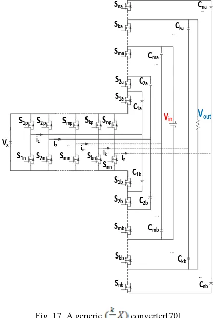
3.8. A generic converter
Figure 17 illustrates the structure and of a generic
converter. It can be seen that the proposed
converter has ‘n’ different arms and ‘n’ different legs leading to a total of ‘2n’ limbs. Each arm is comprised of a series connection of two capacitors and two arm switches labeled with suffixes ‘a’ and ‘b’. For example, arm no. 1 consists of capacitors C1a and C1b connected in series with
switches S1a and S1b. Each leg of the converter consists of
a half-bridge cell composed of two switches switched in a complementary function. Leg 1 consists of S1p and S1n. In
comparison to the double wing structure proposed in [69], it can be observed that an extra degree of freedom with respect to the location of input voltage and output voltage
is introduced in the converter. Both the input
voltage Vin and output voltage can be connected across
any of the ‘n’ arms of the converter. For a generic location of the input voltage, Vin on the mth arm of the converter,
the “effective input” voltage, Vx across Cx can be
expressed as:
(10)
For a generic location of the load across arm ‘K’, the output voltage Vout can then be expressed as:
(11)
Where, m denotes the arm across which the input voltage is connected and k is the arm across which the load is connected where k,m ≤ n. If k > m, the converter functions as a boost converter. Figure 18 also shows that one other degree of freedom can be obtained by placing the source or load across Cx. If the
input voltage, Vin is placed across Cx and the load is
connected across the generic arm, ‘k’ as described above, the output voltage,
(12)
This converter includes the following advantages: An inductor-less, high gain DC-DC converter with a high efficiency and high power density is a much desired circuit in electric vehicle (EV) powertrain and solar photovoltaic (SPV) power converters. Modular multi-level capacitor clamped DC-DC converter circuits (MLCCCs) provide a viable solution for this case. However, their application is limited owing to their limitations in terms of fixed output voltage gains and lack of fractional output gains [70].
Vx
S1p S2p Smp Skp Snp
S1n S2n Smn Skn Snn
S1a S2a Sma Ska Sna
S1b
S2b
Smb
Skb
Snb C1a
C2a Cma
Cka Cna
C1b
C2b
Cmb
Ckb
Cnb Vin
V
outi1 i 2 i
m i k
in
...
... ...
...
...
...
...
Fig. 17. A generic converter[70].
There has also been many multiplier converters made by researchers around the world which, according to the statements of this paper one of them can be used in photovoltaic systems whose advantages and disadvantages can also be discussed.
2
.
1
inx
V
m
V
in x
out V
m k V n
V 2 .
in out
k
V
298
Table 2 Advantages and Disadvantages of Boost converters
Utilized in photovoltai c systems Number of elements
used in the circuit Advantages and Disadvantages
DC-DC Converters
yes Number of inductances: 1 Number of capacitors: 1 Number of diodes: 1 Number of keys: 1 1.Semiconductor power electronic switches with high voltage rate
2.High cost of power electronic switches 3. Large size and larger weight than TBLC.
4. Application in power systems with a low voltage-power rate. Fig. 4. DC-DC
boost converters
yes Number of inductances: 1 Number of capacitors: 4 Number of diodes: 4 Number of keys: 1 1.Increase in power rate
2.Reduction of power ripple
3.Requires more elements than conventional boost converter in circuits 4.Increasing the voltage level only with an inductance
5. The cost of the converter is less than that of conventional boost converters.
6.The disadvantage of the earth separated by the load and the source Fig. 5. Hybrid
boost converters
yes Number of inductances: 1 Number of capacitors:2 Number of diodes: 2 Number of keys: 2 1. Use of power electronic switches, with a lower voltage rate than
conventional boost converters (about half voltage rate of conventional boost converter).
2. Application in power systems with a medium and high voltage-power rate.
3. Reducing the size in inductance filter of TBLC compared with inductance filter of conventional boost converters (about a quarter size of the conventional boost converter).
4. Reducing the capacity of TBLC compared with that of conventional boost converters (about half of the capacity of conventional boost converters). 5. Reducing the current ripple by a quarter.
6. Increasing the frequency of the voltage across the LC filter to double the switching frequency.
7. Decreasing the cost of power switch; Reducing the total weight and size of the converter.
Fig. 6. Three level boost converter
yes Number of inductances: 1 Number of capacitors: 2 Number of diodes: 8 Number of keys: 4 1. The converter's efficiency is about 93 %.
2.The magnitude of duty of the cycle for increasing the voltage is about 0.5 3. Voltage stress on the switch is half the output voltage.
4. Application in power systems with a medium and high voltage-power rate.
5. Decreasing the cost of power switch.
6. Reducing the total weight and size of the converter. Fig. 11. Hybrid
boost three level converter
no Number of inductances: 4 Number of capacitors: 2 Number of diodes: 7 Number of keys: 2 1. The voltage stress of the capacitors, diodes, and power devices is
reduced.
2. The converter has a switching network for the inductor which allows the use of smaller inductors.
Fig. 12. Proposed dc-dc converter
yes
2-Leg:
Number of inductances: 2 Number of capacitors: 2 Number of diodes: 2 Number of keys: 2
4-leg:
Number of inductances: 4 Number of capacitors: 2 Number of diodes: 5 Number of keys: 4 1. Including reduced input current ripple.
2. Benefits of this topology, operating degraded modes lead to undesirable effects such as electrical overstress on components and input increasing current ripple.
Fig. 13-15. FIBC
yes Number of inductances: 2 Number of capacitors: 2n Number of diodes: 2n Number of keys: 1 1. Total advantages of three-level boost converters with more reduction in
switching losses, cost, and weight.
2. The complexity of the converter control is due to increased number of switches.
Fig. 16. Multi-level boost converter
no Number of capacitors: 2 n
Number of keys: 4 n 1.Inductor-less, high gain DC-DC converter witha high efficiency and high
power density
2. Their application is limited owing to their limitations in terms of fixed output voltage gains and lack of fractional output gains.
3. The complexity of control in the photovoltaic system is greater upon increase in the number of switches and applications in the stepper motors, due to the stepped output of the voltage.
Journal of Solar Energy Research Vol 4 No 4 Autumn (2019) 287-299
298 References
[1] Koutroulis Eftichios, Kalaitzakis Kostas, Voulgaris Nicholas C. Development of a microcontroller-based photovoltaic maximum power point tracking control system. IEEE Trans Power Electron 2001;16(1):46–54. [2] Kjaer Soeren Baekhoej, Pedersen John K, Blaabjerg Frede. A review of single – phase grid connected inverters for photovoltaic systems. IEEE Trans Ind Appl 2005;41(5):1292–306.
[3] Jiang Joe-Air, Huang Tsong-Liang, Hsiao Ying-Tung,
Chen Chia-Hong. Maximum power tracking for
photovoltaic power systems. Tamkang J Sci Eng 2005;8(2):147–53.
[4] Ming Zeng, Ximei Liu, Na Li, Song Xue. Overall review of renewable energy tariff policy in China:
evolution, implementation, problems, and
countermeasures. Renew Sustain Energy Rev
2013;25:260–71.
[5] Valkila Noora. Arto saari.Urgent need for new approach to energy policy: the case of Finland. Renew Sustain Energy Rev 2010;14:2068–76.
[6] Stephenson Janet, Ford Rebecca, Nair Nirmal-Kumar, Watson Neville, Wood Alan, Miller Allan. Smart grid research in New Zealand - A review from the GREEN Grid research programme. Renew Sustain Energy Rev 2018;82:1636–45.
[7] Islam M, Fartaj Amir, Ting David SK. Current utilization and future prospects of emerging renewable energy applications in Canada. Renew Sustain Energy Rev 2004;8:493–519.
[8] Nematollahi Omid, Kim Kyung Chun. A feasibility study of solar energy in South Korea. Renew Sustain Energy Rev 2017;77:566–79.
[9] Mígueza JL, López LM, Sala JM, Porteiro J, Granada E, Morán JC, Juárez M. Review of compliance with EU-2010 targets on renewable energy in Galicia (Spain). Renew Sustain Energy Rev 2004;10:225–47.
[10] Yushchenko Alisa, Bono Andrea de, Chatenoux Bruno, Patel Martin Kumar, Ray Nicolas. GIS-based assessment of photovoltaic (PV) and concentrated solar power (CSP) generation potential in West Africa. Renew Sustain Energy Rev 2018;81:2088–103.
[11] Alemán-Nava Gibrán S, Casiano-Flores Victor H, Cárdenas-Chávez Diana L, Rocío Díaz-Chavez, Scarlat Nicolae, Mahlknecht Jürgan. Renewable energy research projects in Mexico: a review. Renew Sustain Energy Rev 2014;32:140–53.
[12] Rawea Adel Saleh, Urooj Shabana. Strategies, current status, problems of energy and perspective of Yemen's renewable energy solutions. Renew Sustain Energy Rev 2018;82:1655–63.
[13] Honrubia-Escribano Andrès, Ramirez FJavier, Gómez-Lázaro Emilio, Garcia-Villaverde Pedro M, Ruiz-Ortega Maria J, Parra-Requena Gloria. Influence of solar technology in the economic performance of PV power plants in Europe. Renew Sustain Energy Rev 2018;82:488–501.
[14] Qin Lijun, Lu Xiao. Engineering Matlab/Simulink-Based Research on Maximum Power Point Tracking of Photovoltaic Generation,2012 International Conference on Applied Physics and Industrial Engineering, Science Direct, Physics Procedia, 24; 2012. pp. 10–18.
[15] Lim Yan Hong, Hamill.Simple DC. Maximum power point Tracker for photovoltaic arrays. Electron Lett 2000;36(11):997–9.
[16] Patel H, Agarwal V. MATLAB-based modeling to study the effects of partial shading on PV array
characteristics. IEEE Trans Energy Convers
2008;23(1):302–10.
[17] R. Hasan and S. Mekhilef, "Highly efficient fly-back micro inverter for grid-connected rooftop PV system,"Solar Energy, vol. 146, pp. 511-522, 2017/04/01/ 2017.
review of technical requirements for plug-and-play solar photovoltaic micro inverter systems in the United States,"
Solar Energy, vol. 135, pp. 455-470, 2016/10/01/ 2016.
[19] N. U. Day, C. C. Reinhart, S. DeBow, M. K. Smith, D. J. Sailor, E. Johansson, et al., "Thermal effects of Micro inverter placement on the performance of silicon photovoltaics," Solar Energy, vol. 125, pp. 444-452, 2016/02/01/ 2016.
[20] Q. Zhao, F. Tao, Y. Hu, and F. C. Lee, "Active-clamp DC/DC converters using magnetic switches," in
Applied Power Electronics Conference and Exposition, 2001. APEC 2001. Sixteenth Annual IEEE, 2001, pp. 946-952.
[21] M. Prudente, L. L. Pfitscher, G. Emmendoerfer, E. F. Romaneli, and R. Gules, "Voltage multiplier cells applied to non-isolated DC–DC converters," IEEE Transactions on Power Electronics, vol. 23, pp. 871-887, 2008.
[22] K.-B. Park, H.-W. Seong, H.-S. Kim, G.-W. Moon, and M.-J. Youn, "Integrated boost-sepic converter for high step-up applications," in 2008 IEEE Power Electronics Specialists Conference, 2008, pp. 944-950. [23] Amir A, Amir A, Che HS, El Khateb A, Rahim NA. Comparative Analysis of High Voltage Gain DC-DC Converter Topologies for Photovoltaic Systems. Renewable Energy. 2018 Sep 27.
[24] Gopi RR, Sreejith S. Converter topologies in photovoltaic applications–A review. Renewable and Sustainable Energy Reviews. 2018 Oct 31;94:1-4. [25] Hossain MZ, Rahim NA. Recent progress and development on power DC-DC converter topology, control, design and applications: A review. Renewable and Sustainable Energy Reviews. 2018 Jan 31;81:205-30. [26] Khosrogorji S, Ahmadian M, Torkaman H, Soori S. Multi-input DC/DC converters in connection with distributed generation units–A review. Renewable and Sustainable Energy Reviews. 2016 Dec 1;66:360-79. [27] de Paula, Arthur Neves, et al. "An extensive review of nonisolated DC-DC boost-based converters." 2014 11th IEEE/IAS International Conference on Industry
Applications. IEEE, 2014.
299
[28] Forouzesh, Mojtaba, et al. "Step-up DC–DC converters: a comprehensive review of voltage-boosting techniques, topologies, and applications." IEEE Transactions on Power Electronics 32.12 (2017): 9143-9178.
[29] V. Salas, E. Oli´s, A. Barrado and A. La´zaro, “Review of the maximum power point tracking algorithms for stand-alone photovoltaic systems,” Solar Energy Materials & Solar Cells 90 (2006) 1555–1578.
[30] Yang JW, Do HL. Analysis and design of a high-efficiency zero-voltage-switching step-up DC–DC converter. Sadhana 2013;38(Part 4):653–65.
[31] Lingle JohnT. Reliable energy conversion power systems for space flight, Supplement to IEEE transactions on aerospace, June; 1965.
[32] Krithiga S, Ammasai Gounden N. Investigations of an improved PV system topology using multilevel boost converter and line commutated inverter with solutions to grid issues. Simul Model Pract Theory 2014;42:147–59. [33] Li W, He X. An interleaved winding-coupled boost converter with passive lossless clamp circuits. IEEE Trans Power Electron 2007;22(4):1499–507, [Jul].
[34] Zhao Q, Lee FC. High-efficiency, high step-up DC–DC converters. IEEE Trans Power Electron 2003;18(1):65–73, [Jan].
[35] Henn G, Silva R, Prac¸a P, Barreto L, Oliveira D. Interleaved boost converter with high voltage gain. IEEE Trans Power Electron 2010;25(11):2753–61, [Nov]. [36] Kwon JM, et al. Three-phase photovoltaic system with three-level boosting MPPT control. IEEE Trans Power Electron 2008;23:2319–27.
[37] Doo-Yong J, et al. Interleaved soft-switching boost converter for photovoltaic power-generation system. IEEE Trans Power Electron 2011;26:1137–45.
[38] Agorreta JL, et al. Fuzzy switching technique applied to PWM boost converter operating in mixed conduction mode for PV systems. IEEE Trans Ind Electron 2009;56:4363–73.
[39] Y. J. A. Alcazar, D. de Souza Oliveira, F. L. Tofoli, and R. P. Torrico-Bascope, "DC–DC non isolated boost converter based on the three-state switching cell and voltage multiplier cells," Industrial Electronics, IEEE
Transactions on, vol. 60, pp. 4438-4449, 2013.
[40] W. Li and X. He, "An interleaved winding-coupled boost converter with passive lossless clamp circuits,"
Power Electronics, IEEE Transactions on, vol. 22, pp. 1499-1507, 2007.
[41] E. H. Ismail, M. A. Al-Saffar, A. J. Sabzali, and A. A. Fardoun, "High voltage gain single-switch non-isolated DC-DC converters for renewable energy applications," in
Sustainable Energy Technologies (ICSET), 2010 IEEE International Conference on, 2010, pp. 1-6.
[42] A. A. Fardoun and E. H. Ismail, "Ultra step-up DC– DC converter with reduced switch stress," Industry
Applications, IEEE Transactions on, vol. 46, pp. 2025-2034, 2010.
[43] Y. Zhao, X. Xiang, C. Li, Y. Gu, W. Li, and X. He, "Single-phase high step-up converter with improved multiplier cell suitable for half-bridge-based PV inverter system," Power Electronics, IEEE Transactions on,
vol. 29, pp. 2807-2816, 2014.
[44] J.-K. Kim and G.-W. Moon, "Derivation, analysis, and comparison of non isolated single-switch high step- up converters with low voltage stress," Power Electronics, IEEE Transactions on, vol. 30, pp. 1336-1344,
2015.
[45] Y. Zhang, J.-T. Sun, and Y.-F. Wang, "Hybrid boost three-level DC–DC converter with high voltage gain for photovoltaic generation systems," Power Electronics, IEEE Transactions on, vol. 28, pp. 3659-3664,
2013.
[46] L. H. S. C. Barreto, P. Peixoto Praca, D. S. Oliveira, and R. N. Silva, "High-voltage gain boost converter based on three-state commutation cell for battery charging using PV panels in a single conversion stage,"
Power Electronics, IEEE Transactions on, vol. 29, pp. 150-158, 2014.
[47] B. Wu, S. Li, Y. Liu, and K. M. Smedley, "A New Hybrid Boosting Converter for Renewable Energy Applications," Power Electronics, IEEE Transactions on,
vol. 31, pp. 1203-1215, 2016.
[48] M. Samadi, S.M. Rakhtala, “Design output control TLB converter for DC drive applications with photovoltaic power supply” Journal of Solar Energy Research, pp.105-110, 2017.
[49] M. Samadi, S.M. Rakhtala,”Reducing cost and size in photovoltaic systems using Three-level boost converter based on fuzzy logic controller” Iran J Sci Technol Trans Electr Eng, 2018 .
[50] Vorobei V, Zakis J, Husev O, Veligorskyi O, Savenko O. Simulation study of the three-level boost DC-DC converter with full ZVS for PV application. In Power Electronics and ECCE Asia (ICPE-ECCE Asia), 2015 9th International Conference on 2015 Jun 1 (pp. 2038-2043). IEEE.
[51] Chen HC, Lin WJ. MPPT and voltage balancing control with sensing only inductor current for photovoltaic-fed, three-level, boost-type converters. IEEE Transactions on Power Electronics. 2014 Jan 1;29(1):29-35.
[52] Zhang Y, Sun JT, Wang YF. Hybrid boost three-level DC–DC converter with high voltage gain for photovoltaic generation systems. IEEE Transactions on Power Electronics. 2013 Aug;28(8):3659-64.
[53] Salary E, Banaei MR, Ajami A. Design of novel step-up boost DC/DC converter. Iranian Journal of Science and Technology, Transactions of Electrical Engineering. 2017 Mar 1;41(1):13-22.
[54] .D. Coutellier, V.G. Agelidis, S. Choi, Experimental verification of floating output interleaved-input DC-DC high-gain transformer-less converter topologies, in: Proceedings of IEEE Power Electronics Specialists Conference (PESC), 2008, pp. 562-568.
[55] S. Choi, V.G. Agelidis, J. Yang, D. Coutellier, P. Marabeas, Analysis, design and experimental results of a floating-output interleaved-input boost-derived DCDC high-gain transformer-less converter, IET Power Electron. 4 (1) (2011) 168-180.
299
Journal of Solar Energy Research Vol 4 No 4 Autumn (2019) 287-299
300
[56] M. Kabalo, D. Paire, B. Blunier, D. Bouquain, M. Godoy Simoes, A. Miraoui, Experimental validation of high-voltage-ratio low-input-current-ripple converters for hybrid fuel cell super capacitors systems, IEEE Trans. Veh. Technol. 61 (8) (October 2012) 3430-3440.
[57] D. Guilbert, A. Gaillard, A. Mohammadi, A. N'Diaye, A. Djerdir, Investigation of the interactions between proton exchange membrane fuel cell and interleaved DC/DC boost converter in case of power switch faults, Int. J. Hydrogen Energy 40 (1) (2015) 519-537.
[58] Guilbert D, Gaillard A, N'Diaye A, Djerdir A. Power switch failures tolerance and remedial strategies of a 4-leg floating interleaved DC/DC boost converter for photovoltaic/fuel cell applications. Renewable Energy. 2016 May 1;90:14-27.
[59] J. C. Rosas-Caro, J. M. Ramirez, F. Z. Peng, and A. Valderrabano, “A dc-dc multilevel boost converter,” IET Power Electronics, vol. 3, no. 1, pp. 129–137, January 2010.
[60] Hafez AAA. Multi-level cascaded DC/DC converters for PV applications. Alex Eng J 2015;54:1135–46, [12//]. [61] Morales-Saldana J, Gutierrez EEC, Leyva-Ramos J. Modeling of switch-mode dc-dc cascade converters. IEEE Trans Aerosp Electron Syst 2002;38:295–9.
[62] Cai W, Fahimi B, Cosoroaba E, Yi F. "Stability analysis and voltage control method based on virtual resistor and proportional voltage feedback loop for cascaded DC-DC converters. In: Proceedings of the energy conversion congress and exposition (ECCE). IEEE; 2014. p. 3016–22.
[63] Kashani MG, Mobarrez M, Bhattacharya S. Variable interleaving technique for photovoltaic cascaded DC-DC converters. In: Proceedings of the 40th Annual Conference of the IEEE Industrial Electronics Society. IECON; 2014. p. 5612–17.
[64] Anurag MB, Thrinath GS, Karanki SB, Yallamili R. Design of ZVS based high gain DC-DC converter for PV
applications. In Renewable Energy Research and Applications (ICRERA), 2016 IEEE International Conference on 2016 Nov 20 (pp. 584-589). IEEE. [65] Remache SE, Barra K. Performance comparison among boost and multi level boost converters for photovoltaic grid connected system using finite set model predictive control. In Renewable Energy Congress (IREC), 2018 9th International 2018 Mar 20 (pp. 1-6). IEEE.
[66] Ahmed ME, Mousa M, Orabi M. Development of high gain and efficiency photovoltaic system using multilevel boost converter topology. InPower Electronics for Distributed Generation Systems (PEDG), 2010 2nd IEEE International Symposium on 2010 Jun 16 (pp. 898-903). IEEE.
[67] Feloups CE, Ali AI, Mohamed EE. Single-phase seven-level PWM inverter for PV systems employing multi-level boost converter. In Innovative Trends in Computer Engineering (ITCE), 2018 International Conference on 2018 Feb 19 (pp. 403-409). IEEE.
[68] Kumar VA, Arounassalame M. PV-FC hybrid system with multilevel boost converter fed multilevel inverter with enhanced performance. In2017 International Conference on Technological Advancements in Power and Energy (TAP Energy) 2017 Dec 21 (pp. 1-6). IEEE. [69] Wei Qian; Dong Cao; Cintron-Rivera, J.G.; Gebben, M.; Wey, D.; Fang Zheng Peng, "A Switched-Capacitor DC–DC Converter With High Voltage Gain and Reduced Component Rating and Count," Industry Applications, IEEE Transactions on , vol.48, no.4, pp.1397,1406, July-Aug. 2012.
[70] Gunasekaran D, Qin L, Karki U, Li Y, Peng FZ. Multi-level capacitor clamped DC-DC multiplier/divider with variable and fractional voltage gain-an (n/m) X DC-DC converter. In Applied Power Electronics Conference and Exposition (APEC), 2016 IEEE 2016 Mar 20 (pp. 2525-2532).

![Fig. 5. Hybrid Boosting Converter [47].](https://thumb-us.123doks.com/thumbv2/123dok_us/8944785.1854153/3.533.39.242.381.515/fig-hybrid-boosting-converter.webp)


![Fig. 9. Two deduced boost three-level dc–dc converters[52].](https://thumb-us.123doks.com/thumbv2/123dok_us/8944785.1854153/6.533.41.243.324.677/fig-deduced-boost-level-dc-dc-converters.webp)
![Fig. 12 The circuit of the new converter[53].](https://thumb-us.123doks.com/thumbv2/123dok_us/8944785.1854153/7.533.39.239.293.491/fig-the-circuit-of-the-new-converter.webp)
![Fig. 15. Floating Interleaved Cascade Boost Converter (FICBC)[58].](https://thumb-us.123doks.com/thumbv2/123dok_us/8944785.1854153/8.533.309.469.42.185/fig-floating-interleaved-cascade-boost-converter-ficbc.webp)