Design of Area Efficient Delay Flip Flop based on
Static 125nm CMOS Technology
S. Gopinath R. K. Gowtham
BE Student BE Student
Department of Electronics & Communication Engineering Department of Electronics & Communication Engineering SNS College of Technology, Coimbatore - 35 SNS College of Technology, Coimbatore - 35
K. Karthick G. Hemanth Kumar
BE Student BE Student
Department of Electronics & Communication Engineering Department of Electronics & Communication Engineering SNS College of Technology, Coimbatore - 35 SNS College of Technology, Coimbatore - 35
G. Naveen Balaji
Assistant Professor
Department of Electronics & Communication Engineering SNS College of Technology, Coimbatore - 35
Abstract
Sequential logic is a form of binary circuit design that employs one or more inputs and one or more outputs, whose states are related by defined rules that depend, inpart, on previous states. In sequential logic the output depends on both present inputs and the past output. Each of inputs and outputs can attain either of two stages: Logic ‘0’ (Low) or Logic ‘1’ (High). A common example of the circuit employing sequential logic is Flipflops or also called as Bistable gate. A simple flipflop has two stable states. The flipflop maintains its states indefinitely until its input pulse called trigger is received. If a trigger is received, the flipflop outputs change their states according to the defined rules, and remain in that states until another trigger is received. There are different kinds of flipflops are available such as D,T,J-K,S-R flipflops in the form of logic gates. The basic D flipflop has a D(data) input and a clock input and outputs Q and Qbar .Optionally it may also include the Reset and the Clk inputs.
Keywords: D flip flop , CMOS, Static CMOS, 125nm, Tanner, Multisim, Xilinx, Half Adder, Full Adder, Sequential Circuit, Combinational Circuit, PMOS, NMOS, Metal Oxide Semiconductor
_______________________________________________________________________________________________________
I. INTRODUCTION
A D-FLIP FLOP is a clocked flip-flop which as two stable states which operates in the delay time in a input by clock cycle. Delay circuits are created by cascading many D-type flip flops. It can be used in many applications such as in digital television systems. A D-flip flop is also called as D flip flop or delay flip flop .D type flip flop consists of four inputs are Data input, Clock input, set input, reset input. It has two outputs and it is being logically inverse of other .The data input is 0 or 1which mean low or high voltage. To synchronize input of the clock signal is needed to the external signal. The input and output are set at low. It has two possible values. Input D=0,flipflop undergoes a reset, that is the output will be set to zero, and input D=1,it does a set ,and the output is1. In the latch clock signal is not provided because D flip flop differs from D- type latch. To change the states D type D flip flop signals are needed. A pair of SR latches and with the inverter connection between S&R inputs single data input, it can be both high or low at the same time. Salient features of D flip flop is the ability to latch and store and remember the data. It ios used in creating the data in the circuit used. Applications of D flip flop it is used in several types in frequency dividers and data latches. Role of flip flop in sequential circuits are, A flip flop is a sequential circuit which samples the input & changes the output at the particular instance of time .It has two stable states ans can be used to store the state information. Singals are applied to one or more, control inputs to change the state of the circuit and will have one or two outputs.
solutions are used in a renge of applications in power management, next- generation wireless, consumer electronics, displays and imaging, life sciences, automotive and RF market segments.
II. EXISTING SYSTEM
A full adder proceeds two binary numbers plus a carry or overflow bit. The output is a sum and carry bit. full adders are generally linked to each other to append bits to a arbitrary length of bits such as 32 or 64 bit. A full adder is competently two half adders an ‘XOR’ and an ‘AND’ gate connected by an ‘OR’ gate. Half adder is a digital circuit that executes summation of numbers. The half adders adds two binary digits called as augend and addend and bring forth two outputs as sum and carry , ‘XOR’ is appertained to both input to produce sum and ‘AND’ gate is appertained to both inputs to produce carry . A Half Adder is made up of multiple gates which performs very basic operations according to the connections made in the CMOS (Complementary Metal Oxide Semiconductor
Gates used in the Carry Skip Adder are ‘xor’ gate, ‘and’ gate, ‘not’ gate. Generally gate are the building blocks of the the combinational circuits .Gates are built using several numbers of transistor. We know that Moore’s law which states every six months number of the transistors used in a particular integrated circuit will be increased due to the technology enhancement. The XOR gate is a combinational logic gate that gives a ‘1’ output when the number of ‘1’ inputs is odd. An XOR gate implements an exclusive or, that is, a ‘1’ output results if one, and only one, of the inputs to the gate is ‘1’. If both inputs are ‘0’ or both are ‘1’, a ‘0’ output results. In ‘and’ gate ,only multiplication operation can be done if the both input are same the output will be the same as the input and if the inputs are different then the output will ‘0’. In ‘not’ gate, contains only one input and the output is the output of the input if the input is ‘1’ then the output will be ‘0’ vice versa.
Fig. 1.1: Block diagram of Half Adder:
In Fig 1.1 we can analyze that a half Adder consist of two inputs ‘a’ and ‘b’ and output ‘sum’and ‘carry’. Carry Skip Adder is buildup of multiple full adders and full adders are made with two half adder A truth table is a logically based mathematical table that expatiates the conceivable sequels of scenario the truth table suppresses the truth values thar would appear under the premises of the given scenario. The rows of a basic truth table contain the Boolean logic true or false values while the columns list the premises of a scenario as well as conclusion.
Fig. 1.2: Logic diagram of Half Adder:
In fig 1.2 Gates like ‘xor’ , ‘not’, and ‘and’ Gates which are used to process the inputs and give the output. Each gate has a difference type of process algorithm based the connection given to the CMOS. The Boolean expression of the half Adder is as follows.
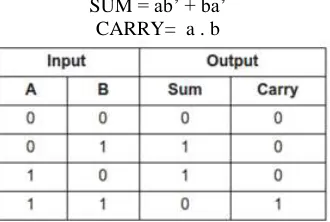
SUM = ab’ + ba’ CARRY= a . b
In Fig 1.3 is a truth table of the half Adder which portrays the output of that logical circuit . A half Adder is a basic arithmetic processor which perform only subtraction its only function is to deduce a single bit binary from the input
III. DELAY FLIP FLOP
A simple flipflop has two stable states. The flipflop maintains its states indefinitely until its input pulse called trigger is received. If a trigger is received, the flipflop outputs change their states according to the defined rules, and remain in that states until another trigger is received. There are different kinds of flipflops are available such as D,T,J-K,S-R flipflops in the form of logic gates. The basic D flipflop has a D(data) input and a clock input and outputs Q and Qbar .Optionally it may also include the Reset and the Clk inputs.
Fig. 2.1: Block diagram of D – Flip Flop
In Fig2.1 we can analyze that a D-FlipFlop consist of one input ‘D’, whereas output ‘Q’and ‘Q`’
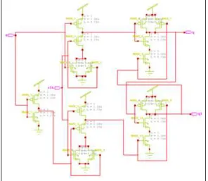
Fig. 2.2: Logic Diagram of D-Flip Flop
In Fig 2.2 When the inputs are given through the respective labels gates present the circuits will process the data and perform the Delay Operation and produce the Respective output ‘Q’and ‘Q`’.
In Fig 2.3The above D - Flip Flop is designed using static cmos algorithm under 125 nm which is quite efficient and the results are same as the currently existing one When the inputs are given through the respective labels gates present the circuits will process the data and perform the delay operation and produce the Respective output ‘Q’and ‘Q`’
IV. RESULTS
Output
Waveform of Logic design of D-Flip Flop:
Waveform of CMOS design of D-Flip flop:
V. CONCLUSION
REFERENCES
[1] N.Weste and K.Eshraghian,--Principles of VLSI Design,A system perspective,Reading,MA:Addison-Wesley,1993.
[2] Shital Baghel, Pranay Kumar Rahi,Nishant Yadav,2015,”(CMOS) Half Adder Design & Simulation Using Different Foundry”, International al Journal
of Innovative Science, Engineering &Technology(IJISET),Vol.2 Issue 3, pp.195-622,Aug.2000.
[3] Ming-Bo Lin, “Introduction to VLSI systems A logic, circuit and system perspective,” Taylor & Fransis group,ch. 7
[4] Neil H.E.Weste, DavidHarris and Ayan Banaerjee,”CMOS VLSI Design”. Pearson Education,Inc.,pp.11,Third edition,2005.
[5] M. Morris Mano, Michael D. Cilleti “Digital Design”,4th edition,pp.143,2012.
[6] Kaushik Roy and S.C.Prasad,”Low power CMOS VLSI circuit design”,Willey,pp.1-129,2000
[7] E.M.M.Poncino,(1996)Power Consumption of Static and Dynamic CMOS circuits, IEEE,2nd International Conference on ASIC,pp.425-427.
[8] P.S.Aswale and S.S.Chopade,(2013) Comparative Study of Different Low Power Design Techniques for reduction of Leakage power in CMOS VLSI
Circuits,IJCA(0975-8887,Volume 70-NO.1
[9] R.L.Geiger, P.E.Allen, N.R.Strander(2013) VLSI Design techniques for Analog and Digital Circuits, McGraw Hill,New Delhi,India,.[page.No.597-ch7
[10] S. Shobana, R. Ramya, K.K. Rashika, G. Naveen Balaji, K. Boopathiraja, “Hamming Window Function based FFT Analysis of Advanced Approximate
Adder design in 125nm CMOS technology using Transmission gates”, International Journal of Science and Innovative Engineering & Technology, Vol. 5, Issue: May 2018.
[11] G.NaveenBalaji,P.Malini,T.Poovika, P.Shanmugavadivu, “14T Full Adder in 125nm CMOS technology for FFT applications using piecewise constant