International Doctorate School in Information and Communication Technologies
DISI - University of Trento
Ultra-low-power
Wireless Camera Network Nodes
Design and Performance Analysis
Leonardo Gasparini
Advisor:
Prof. Dario Petri
Universit`a degli Studi di Trento
Co-Advisor:
Dr. Massimo Gottardi
Fondazione Bruno Kessler
and the Prince
and secretly,
to the lovely being
with whom I share the shelter
A methodology for designing Wireless Camera Network nodes featuring
long lifetime is presented. Wireless Camera Networks may find widespread
application in the fields of security, animal monitoring, elder care and
many others. Unfortunately, their development is currently thwarted by
the lack of nodes capable of operating autonomously for a long period of
time when powered with a couple of AA batteries. In the proposed
ap-proach, the logic elements of a Wireless Camera Network node are clearly
identified along with their requirements in terms of processing capabilities
and power consumption. For each element, strategies leading to
signifi-cant energy savings are proposed. In this context, the employment of a
custom vision sensor and an efficient architecture are crucial. In order to
validate the methodology, a prototype node is presented, mounting a smart
sensor and a flash-based FPGA. The node implements a custom algorithm
for counting people, a non trivial task requiring a considerable amount of
on-board processing. The overall power consumption is limited to less than
5 mW, thus achieving a two orders of magnitude improvement with respect
to the state of the art. By powering the system with two batteries providing
2200 mAh at 3.3 V, the expected lifetime of the system exceeds two months
even in the worst-case scenario.
Keywords
Wireless Sensor Network, ultra-low-power, vision sensor, FPGA, power
1 Introduction 1
2 State of the Art and Related Work 7
2.1 Commercial, Off-the-Shelf Products . . . 9
2.1.1 Image sensors . . . 9
2.1.2 Processing devices . . . 9
2.1.3 Wireless transceivers . . . 14
2.1.4 General purpose motes . . . 16
2.2 Related Work . . . 18
2.2.1 Panoptes . . . 18
2.2.2 Cyclops . . . 20
2.2.3 Philips Smart Camera Mote . . . 21
2.2.4 MeshEye . . . 22
2.2.5 Yale’s AER imager-based node . . . 24
2.2.6 Other nodes . . . 25
3 Designing an Ultra-Low-Power WCN Node 31 3.1 Hardware . . . 31
3.1.1 Control unit . . . 33
3.1.2 Imager . . . 33
3.1.3 Memory . . . 35
3.2 Firmware . . . 41
3.3 Power Consumption Model . . . 47
4 Implemented Node Architecture 53 4.1 Hardware . . . 55
4.1.1 Sensing . . . 55
4.1.2 Control, storage and processing . . . 59
4.1.3 Communication . . . 60
4.2 Firmware . . . 60
4.2.1 An Integrated People Counter . . . 64
4.3 Power Measurements and Lifetime Estimation . . . 85
5 Conclusion 93
2.1 Processing devices - Summary table . . . 13
4.1 Compression ratios . . . 64
4.2 Classification performances (Mothers intervals removed) . . 77
4.3 Classification performances (Mothers intervals included) . . 77
2.1 Three popular COTS motes by Moteiv/Memsic . . . 16
2.2 Examples of WCN nodes present in the literature . . . 18
2.3 More examples of WCN nodes present in the literature . . 23
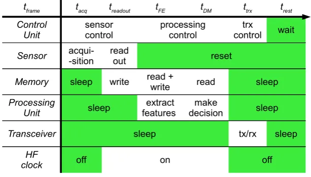
3.1 Control Unit: flowcharts . . . 42
3.2 Idle frame period: status of the node’s elements . . . 43
3.3 Active frame period: status of the node’s elements . . . 45
4.1 Block scheme of the proposed video-node . . . 55
4.2 GrainCam vision sensor . . . 56
4.3 Detecting edges with the employed sensor . . . 58
4.4 Detecting motion with the employed sensor . . . 59
4.5 Sensor-to-FIFO interface . . . 61
4.6 Camera node setup & VIL definition . . . 65
4.7 A sequence of frames of Mout . . . 66
4.8 Insertion of a new node in the multigraph . . . 72
4.9 Node FIFO memory . . . 78
4.10 Segment generation . . . 79
4.11 Calculation of the maximum cost path to node σn+1 . . . . 82
4.12 Edge FIFO memory . . . 84
4.13 Prototype node . . . 86
4.14 Python GUI . . . 87
Introduction
A Wireless Sensor Network (WSN) node (often referred to as just mote) is
an autonomous computing system that is equipped with one or more
sen-sors and that operates in absence of infrastructure, i.e., it is not connected
to the power network and it communicates with other devices through a
wireless channel [1]. Unlike the wired counterpart, with a WSN we can
place the nodes very close to the phenomenon being monitored, without
caring about the nodes positioning as long as the number of sensors
pro-vides enough information to filter out erroneous measurements. The
ac-quired data are then processed on the node before being transmitted to a
data collector which merges the pieces of information for analysis purposes
or to generate an output, typically consisting on an alarm message or a
command for some actuators.
Fields of application include, but are not limited to, the environmental
monitoring (e.g., tracking the movement of animals, or acquiring
informa-tion about the status of the soil for agricultural purposes), health control
(e.g., recording the physiological activity of a living being, which moves
and therefore cannot be connected to the infrastructure through wires),
elder care (e.g., detecting people that fall on the ground and are not able
acquiring information about unexplored terrains).
This thesis deals with Wireless Camera Networks (WCNs), a subclass
of WSNs in which the sensing element is an imager. WCN may find
widespread application in fields such as security, assisted living, road traffic
monitoring, and natural sciences, and offer a number of advantages with
respect to standard wired camera networks [2]. In particular, they are
much easier to deploy and to remove, thus reducing installation time and
costs. This is important for applications that require high density of
place-ment, either to obtain many different views of the scene, or for increased
robustness. Impromptu surveillance installations (for example, to monitor
a building during a special event or animals in their natural habitat) also
require fast installation, re-positioning and removal of a possibly large
num-ber of cameras, and thus would benefit from wireless technology. In-home
elder care and home security may be facilitated by camera monitoring, and
the use of wireless nodes would allow for discreet and unobtrusive
instal-lations at no costs, since the intervention of an operator is not needed [3].
WCNs represent a convenient solution also in those situations in which an
external power source is unavailable or very expensive to provide, such as
in borderlands and dangerous zones. For example, obtaining low voltage
power supply from high-voltage power lines may increase the price of the
wired surveillance system by a factor of 10. Finally, we note that WCNs
are largely immune to failure of the power distribution system, and thus
may support back-up of wired systems in the case of natural or man-made
disasters.
Typically, a WSN node either operates on batteries or extracts the
en-ergy it needs from the environment, thus dictating the employment of
ultra-low-power components to achieve a long lifetime. Of course, the
lim-ited energy resources affect the processing capabilities of the node, but this
acquisitions are performed at low rates. This is the case for temperature,
pressure and humidity measurements, for example. In general, the average
power consumed by the sensing and processing units is limited to less than
a milliwatt and most of the power is spent for wireless communication.
This condition is not true anymore when the sensing unit is a video
sen-sor, which is much more complex and power-demanding than other sensors
such as the ones that measure temperature, pressure or humidity. Not only
the sensing process itself is more expensive (as the imager is composed of an
array of thousands or millions of sensors), but also data buffering,
process-ing and transmission require much more power. At the moment, no feasible
energy scavenging system exists that can provide enough power and the
use of batteries seem the only viable solution. Unfortunately, in this
con-text, batteries have a very limited energy budget, resulting in a trade-off
between the system’s lifetime (typically dictated by the application) and
the desired computational power to process the data. Thus, video nodes
must be designed by carefully selecting the hardware components and by
producing high-efficiency embedded software.
In the past decade, several WCN nodes have been proposed [4,5,6,7,8],
but they have either high power consumption or limited performance.
These systems employ standard imaging sensors, which are typically
de-signed “for humans”, providing high resolution images with several bits
per pixel. Better energy efficiency is achieved by decreasing the sensor
resolution, as long as the resolution is enough for the task at hand [5, 7].
Nevertheless, transmission of the full video stream via IEEE 802.11 or
Bluetooth still requires too much power to be viable. Hence, a certain
amount of on-board processing is necessary, but also data processing is
expensive in terms of power, and it introduces a latency that may reduce
the effective frame rate.
use of standard imagers, which are not necessarily the optimal solution for
a WCN node. In fact, in most cases only particular portions of the image
(such as moving areas, or objects in the foreground) or features (edges,
corners, histograms of brightness or color) are of interest. This suggests
the use of custom imagers that only acquire the data one is interested in,
thus saving energy in the acquisition and in the processing phases. In such
a framework, a new approach to the design of video sensors has been
re-cently proposed by Teixeira et al. [9], one that attempts to limit power
requirements by implementing the processing (or some parts of it) directly
on-chip, thus allowing the entire system to save considerable amount of
power and time. One step further is presented in [10], where the authors
suggest the development of sensors able to perform object detection
au-tonomously, with a very limited external control.
This thesis proposes a design methodology for very low-power WCN
nodes based on this kind of sensors [11]. By pre-processing the images
di-rectly on chip, less data is generated, thus reducing power at multiple levels
(less data to transfer, buffer, and process). Nevertheless, the problem is
still challenging because even running algorithms on already pre-processed
data is a power consuming task. The components present on the node
need to operate with a very limited energy budget and at the same time
to have enough computational capabilities to execute the algorithms in a
short period of time. The solution to the problem is not unique and needs
to be faced from different standpoints. On the one hand, one must identify
which are the components that best fit the case at hand, having clear in
mind how to exploit the resources they provide; on the other hand, one
must implement efficient algorithms on the basis of the images generated
by the sensor and of the available hardware, power and timing resources.
These are concurrent aspects that one has to consider as a whole. We
the characteristics they need to have in order to maximize the network
lifetime, as long as the provided performance suits the application.
Ac-cordingly, we have proposed power-saving strategies that guide the design
process by defining the choices about the hardware components and the
firmware implementation. The key element lays in developing within the
firmware techniques to exploit the low power capabilities offered by the
hardware.
To validate the proposed methodology, we have created a prototype
WCN node. Such prototype exploits an ultra-low-power binary
contrast-based imaging sensor that also features on-chip frame differencing [10].
The node core is represented by a flash-based Field Programmable Gate
Array, which manages the system and processes the data generated by the
sensor. Techniques to limit power consumption have been applied in a
real situation. We have designed the node to operate as a People Counter,
which has been used as a case study. In the end, the prototype’s power
consumption has been analyzed, and we have proved that the node can
operate autonomously for more than a month when powered with a couple
of standard batteries, which is two order of magnitudes longer than the
other camera nodes proposed by the research community.
The proposed approach is suitable for many applications, but we are
aware of its limitations. Of course, we cannot expect an ultra-low-power
node to provide as many details as a standard wired video network.
Nev-ertheless, our solution may play a fundamental role also in an advanced
wireless surveillance system, in which the network is constituted by
hetero-geneous nodes [12]. Such kind of networks are organized hierarchically in
multiple tiers, in which nodes belonging to the lower tiers are in charge of
detecting the presence of some event of interest in the scene and possibly
of localizing it. Such nodes are always active and therefore must consume
is generated for the higher tiers, where nodes equipped with high
resolu-tion imagers process the frames with complex algorithms and, in case the
situation requires the intervention of a human operator, transmit them. In
this way, power is optimized since intensive processing is performed only
when really needed. In this context, the lowest tiers determine the lifetime
of the network, since they operate unceasingly until their power source is
depleted, but, at the moment, no camera node seems to have the
charac-teristics to fill such a role in the network. As a result, WCNs’ lifetime is
limited to few days, thus obstructing the development of this technology,
especially in the commercial sector. We believe that our solution represents
the answer to these needs.
The thesis is organized as follow. In Ch.2we provide the state of the art
about low power WSN systems which are commercially available and about
other hardware solutions which one needs to take into account when
de-signing an ultra-low-power WCN node. We also provide some background
about other existing WCN nodes as reported in the literature, pointing
out their strong and weak points. In Ch. 3, we describe our general design
methodology for an ultra-low-power WCN node, both from the hardware
and the firmware points of view. We provide the detailed power model
for a generic node designed according to our method as well. In Ch. 4 we
describe the architecture of the prototype node that we developed. The
chapter is structured following the design method, getting into the details
of the hardware and firmware aspects. Then, the implemented People
Counter is described firstly from a high level point of view, and then in its
hardware implementation. Power requirement analysis and lifetime
esti-mate of this node are presented in the last part of the chapter. Ch. 5 has
State of the Art and Related Work
This thesis main goal is to provide a method for designing WCN nodes
capable of operating for long periods with a very limited power source. In
pursuing this goal , in this chapter we will concentrate on the system’s
hardware configuration rather than on other aspects such as the network
communication architecture, sensor network topology, energy scavenging
methods, etc. Generally speaking, “a sensor node is made up of four basic
components: a sensing unit, a processing unit, a transceiver unit and a
power unit” [1]. In the following we will consider just the first three of
them, since those are the ones of major interest from the system designer’s
point of view. This is because we expect the system to guarantee proper
functionality continuously for a certain period of time, disregarding what
the power source is, as long as it provides a given (small) capacity.
Several solutions are offered by the market and by the research
commu-nity to develop a wireless node. One may choose to buy a commercial,
off-the-shelf (COTS) node platform (typically including the processing unit,
the transceiver and expansion ports for the sensors), which provides an
in-tegrated environment for fast and easy development. Nevertheless WCNs,
and ultra-low-power WCNs in particular, have critical requirements with
do not provide sufficient processing power to run the algorithms or the
available processor are too expensive in terms of energy to run
continu-ously, clocked at high frequency. Therefore researchers opted for
develop-ing their own custom platform, thus achievdevelop-ing a node highly fitted to the
application. Such platforms may be either stand-alone modules including
all the four basic components, or daughter boards which integrate the
sen-sor and processing units and have to be attached to a COTS host-node,
which takes care of interfacing the sensor with the network. Nevertheless,
we will see that there is a lack of ultra-low-power nodes in the field, and
no WCN node, an therefore no WCN either, seems to be able to operate
on batteries for a long time without replacing the power source.
In this chapter we are going to present a roundup about the state of the
art in individual devices and in host-nodes for WCNs, and discuss about
the related work in the field. This chapter is organized as follows. In the
first part we will briefly introduce the most popular low-power cameras,
field programmable devices and wireless transceivers, and general purpose
WSN host-nodes available in the market. Then we will concentrate on
complete WCN nodes present in the literature that brought original ideas
from the architectural point of view, aiming at lowering power
consump-tion and improving power efficiency, without compromising the network
effectiveness. Since a great variety of hardware platforms were developed
by the research community in the past 10 years, we will concentrate on the
few nodes which in our opinion effectively introduced important
improve-ments in the field. The other relevant nodes will be briefly mentioned at
2.1
Commercial, Off-the-Shelf Products
2.1.1 Image sensors
As we will see later in this chapter, most of WCN nodes employ
OmniVi-sion CMOS camera modules. OmniViOmniVi-sion is a company founded in 1995
and headquartered in Santa Clara (CA, USA), that designs CMOS sensors
and camera modules. Products range from sub-VGA cameras to HD
de-vices. Within the low-range product series, OmniVision cameras provide
low power consumption, around 100 mW at quite high frame rates, 30 to
60 fps. Acquisitions at different resolutions are possible too. Moreover,
their camera modules provide easy interfacing, automatic image control
functions and basic image manipulation inside the module itself. As an
example, the OV6680 [13] includes a CMOS camera providing images at a
resolution that ranges from CIF up to 400×400 pixels, and exhibiting an
active power consumption of 70 mW at 30 fps, CIF format, and a standby
current lower than 20 µA.
Other solutions that suit WCN applications are all those cameras that
can be mounted on mid-range cellphones, such as the old VS6524 [14],
released by ST MicroElectronics in 2004.
2.1.2 Processing devices
The market of processing devices is huge. A great multitude of solutions
from several companies are available to design a camera node. Mainly, we
can distinguish between four classes of processing devices: low-power
mi-crocontrollers, high performance ones/embedded processors, Complex
Pro-grammable Logic Devices and low-power Field ProPro-grammable Gate Arrays.
microprocessor executing a software stored into a ROM. The more
ad-vanced modules often run an Operating System (OS), specifically designed
for embedded systems, that manages the processes on that processor,
in-cluding the access to hardware resources. Lately, multi-core processors
have been introduced in the market, slightly relieving the “one instruction
at a time” limitation introduced by the presence of a single processing core.
A MicroController Unit (MCU) is a single integrated circuit that
con-tains a processor, memory and a set of peripherals such as counters,
watch-dog timers1, multipliers, dividers, ADCs and DACs, and many more. Low
power modes are typically supported, too. The number of available
con-figurations are countless. One may choose a MCU based on a 8-, 16-, or
32-bit architecture and clocked at a speed that ranges from a few kilohertz’s
to hundreds of megahertz’s; MCUs are available with different amounts of
flash ROM to store the program instructions and SRAM for data buffering,
ranging from a few bytes to a few megabytes. Power consumption varies
accordingly, from less than a milliwatt, as in the 8 bit PIC10 series by
Microchip Technologies [15], to hundreds of milliwatts, as in the dual core
32 bit Qorivva device by Freescale Semiconductor [16].
Embedded processors can be seen as high performance MCUs or as
low-power processors, and in fact they represent the boundary between the two
classes. An example is given by Marvell’s PXA3xx family of processors [17],
which can operate at more than 800 MHz clock frequency, include up to
768 Kbytes of internal SRAM and 32 + 32 KB of cache for instructions and
data. Available peripherals include counters, watchdog timers and pulse
width modulators and the chip features all types of interfaces, including
one for a camera. Of course all these properties come at the price of a
higher power consumption with respect to low-power MCUs: at maximum
1A watchdog timer is a timer that generates a system reset every time it overflows. It is used to avoid
speed the processor consumes several hundreds of milliwatts. Even more
powerful devices are considered embedded processors; among these there
is the Intel Atom Processor [18], but in this case consumption increases
significantly, exceeding the watt.
Complex Programmable Logic Devices (CPLDs) and Field
Program-mable Gate Arrays (FPGAs) are two classes of ProgramProgram-mable Logic
De-vices (PLDs) which are typically programmed in Hardware Description
Language (HDL), namely VHDL or Verilog. They contain a matrix of
configurable logic blocks, which in an FPGA typically contain Look-Up
Tables (LUTs), flip-flops, MUltipleXers (MUXs) and other logic. Such
ba-sic elements can be configured and routed “on the field” to carry out the
required task. Since VHDL and Verilog are languages describing hardware
at a lower abstraction lever with respect to programming languages such
as Java, C and even Assembly, writing the code for a CPLD/FPGA is
much more time consuming than a processor. Nevertheless such devices
allow to overcome many of the limitations that processors have, even the
multi-core ones. Consider a simple processor: it has a well defined
ar-chitecture that we cannot change, and the processor core executes all the
instructions sequentially, one after the other. Moreover, only one
periph-eral at a time can write on the bus, since it is shared. As a consequence,
a processor core executes far less than one instruction per clock cycle.
Programmable logic devices are different in the sense that they allow to
configure the internal logic, and it is the programmer’s task to create the
architecture of the processing unit. This allow to write highly optimized
code, and to design processing units which overcome the “one clock-cycle
per instruction” limit imposed by processors, thus boosting the system’s
performance. Furthermore, the manufacturers of PLDs provide tools for
the generation of complex and customizable structures such as First In,
automatic fashion. Since these structures are built exploiting the
config-urable blocks, they are called “soft”-cores, in contrast with the “hard-”,
unchangeable counterparts, printed on silicon.
CPLDs and FPGAs are built on different technologies and their basic
blocks are designed with different goals in mind; from a general, high level
perspective, FPGAs, even the low-power ones, allow for much bigger
de-signs and improved performance with respect to CPLDs, which, on the
other hand, are cheaper and consume less power. Moreover, FPGAs are
typically volatile, therefore they require some additional logic when they
are turned on in order to be programmed, while CPLDs are non-volatile,
thus enabling a significant reduction in system complexity. Lately,
flash-based FPGAs has been introduced in the market, filling the gap between
standard FPGAs and CPLDs.
From the perspective of WCNs, each class has its own pros and cons,
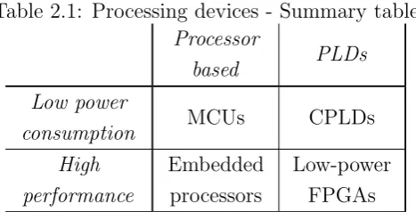
which we try to summarize here and in Tab. 2.1.
Processor based devices are relatively easy to program, especially when there is an OS that manages the resources to avoid conflicts;
on the other side, the presence of a few processing elements and a
sin-gle bus introduces significantly latency delays, which could severely
limit the performance of a WCN node. Another negative aspect is
represented by the limited amount of memory which typically
char-acterizes these devices, thus forcing the employment of an additional,
external element serving both as interface between the sensor and the
processor and as a temporary buffer while processing the data.
PLDs allow to generate an architecture fitted to the application and in which tasks are executed in parallel without the risk of long latency
delays and conflicts among the implemented entities. As a drawback,
Table 2.1: Processing devices - Summary table
Processor
based PLDs
Low power
consumption MCUs CPLDs
High performance
Embedded processors
Low-power FPGAs
writing the code increases exponentially with the complexity of the
design. Nevertheless, manufacturers provide soft-cores which are
be-coming easier and easier to use, thus limiting the difficulties introduced
by the use of HDL.
Low-power MCUs and CPLDs consume very little power, and have been widely used in standard WSNs. Nevertheless, their limited
pro-cessing capabilities may constitute a problem in WCNs, due to the
huge amount of data (represented by the images) that needs to be
processed.
Embedded processors and low-power FPGAs seem to respect the high processing power requirements set by WCNs, but may not be able to
operate for a long period of time due to their elevate power
consump-tion.
Mixed solutions, such as the combination of a low-power MCU and an FPGA, introduce more flexibility and allow to overcome the
limi-tations introduced by the single devices; the disadvantage lays in the
fact that the entire system is more complex to design and power
con-sumption may increase due to the higher activity on input and output
pads.
In conclusion, the choice of the hardware devices responsible for
the complexity of the algorithms that need to be executed by the node, and
by requirements in terms of acquisition rate, latency and lifetime imposed
by the application.
2.1.3 Wireless transceivers
There are mainly four wireless technologies that are considered in the
devel-opment of low-power systems: ZigBee, Bluetooth, Wi-Fi, and Ultra Wide
Band [19]. The ZigBee protocol is universally accepted as the protocol that
best suits for WSNs. This is because it exhibits ultra-low-power
capabil-ities and at the same time enables to build wireless mesh networks, i.e.,
networks in which all devices are actively involved in the network
construc-tion, as “they dynamically join the network, acting as both user terminals
and routers for other devices, consequently further extending network
cov-erage” [20]. The Bluetooth protocol provides higher data rates (1−3 Mbps
vs 250 kbps), but is more oriented towards “short-range and cheap devices
to replace cables for computer peripherals” [19]. This is because Bluetooth
does not support Mesh networks as ZibBee, but piconets and scatternets.
Piconets are networks in which one master device manages the connection
among itself and several slave devices. In this configuration, each slave
de-vice can communicate only with the master. Scatternets are composed by
several interconnected piconets. The rigidity imposed by the master-slave
configuration makes Bluetooth unsuited for WSNs. Wi-Fi and UWB may
be of interest for camera-based SNs. In fact, ZigBee is efficient only when
the amount of transmitted/received data is low, so that the transceiver
is mostly idle. But when we need to transmit images or, even more, to
stream videos, Wi-Fi and UWB are much more power efficient [21, 22],
i.e., they exhibit a lower consumption per bit transmitted. Nevertheless,
these products exhibit a higher absolute power consumption, which makes
The market leader of low-power wireless transceivers, based on the
Zig-Bee/IEEE 802.15.4 standards, is ChipCon. ChipCon is a Norvegian
Com-pany founded in 1996, and acquired by Texas Instruments in 2006, which
became popular for its CC1xxx and CC2xxx families of low-power wireless
transceivers. The CC1xxx family operates in the 300−1000 MHz frequency
range while the CC2xxx one is IEEE 802.15.4 compliant [23], operating at
2.4 GHz. The most popular chips are the CC1000 [24] and the CC2420 [25], which are widely employed in WSN nodes thanks to their low current
con-sumption (7.4/10.4/0.8 mA for the former and 19.7/17.4/0.8 mA for the latter, while receiving, transmitting and being idle respectively), support
for low-power modes, high flexibility in the configuration and small form
factor. The provided data rates are 76.8 kbps for the CC1000 and 256 kbps for the CC2420. Lately, Texas Instruments released the CC2500 [26], an
improved version of the CC2420, achieving higher power efficiency.
Another important player is Nordic Semiconductor. Nordic
Semicon-ductor ASA is a Norwegian company headquartered in Oslo, that operates
in the field of wireless communication and multimedia. This company
pro-poses ultra-low-power solutions that exhibit performance similar to
Chip-Con devices; nevertheless the are not part of the ZigBee Alliance, meaning
that they developed their own technology, still based on the IEEE 802.15.4
standard.
Texas Instruments manufactures Bluetooth devices also, such as the
CC2540 [27]. Power consumption is in the same order of magnitude as the
ZigBee-based solutions; in fact it draws 19.4 mA in reception mode, 24 mA in transmission mode and much less than 1 mA when exploiting one of the
low-power modes. Recently, a new, Bluetooth-based, ultra-low-power
de-vice has been introduced by Nordic Semiconductor: the nRF8001 [28]. This
(a) Tmote Sky/TelosB (b) MicaZ (c) iMote2
Figure 2.1: Three popular COTS motes by Moteiv/Memsic
2.1.4 General purpose motes
Moteiv, from San Francisco (CA, USA), is a company that operates in the
field of WSN. Moteiv main product is the Tmote Sky. Moteiv was founded
by three University of California, Berkeley (UCB) Ph.D. students in 2003.
Since 2006 Moteiv became a subsidiary of Sentilla, a Redwood City (CA,
USA)-based company operating in the field of energy. Memsic is another
company from Andover (MA, USA) founded in 1999, which is currently the
world leading supplier of wireless sensor technology. They provide several
wireless modules as host nodes for WSN: TelosB, MICA2 and MICAz,
and iMote2, which were originally manufactured by CrossBow, another
American company operating in the field of smart-sensor technology.
Tmote Sky [29] is an ultra-low power host-mote, equipped with a Texas Instruments MSP430 Microcontroller [30] and a Chipcon CC2420
RF transceiver. The MSP430 is based on a 16 bit RISC architecture and
is designed to operate at low frequencies, in the order of 1 MHz. It is
widely used in WSNs, since it provides very high flexibility in terms of
power consumption: five different power modes are supported, with a
measurements, and allows to attach other devices through two expansion
connectors. From the firmware point of view, the system runs TinyOS, a
light yet efficient open source operative system, developed at University of
California, Berkeley, USA. TelosB [31] is the same design.
MICA2 [32] and MICAz [33] are slightly more computationally pow-erful then TelosB, at the price of a higher power consumption. An Atmel
ATmega128L [34] represents the core of the node: it is an 8-bit, RISC
based MCU, clocked at up to 8 MHz, and draws no more than 20 mA
in active mode. It supports six different sleep modes, which allow to
re-duce power consumption down to a few micro-Watts, when the resources
are not needed. MICA2 and MICAz provide respectively a 868/916 MHz
multi-channel transceiver (the Chipcon CC1000), and an IEEE 802.15.4
compliant RF one (the Chipcon CC2420), but do not have any sensor
al-ready present on board; access to external devices is achieved through two
expansion connectors. These nodes run a TinyOS based operative system
called MoteWorks.
iMote2 [35, 36] is well above the previous nodes in terms of processing capabilities thanks to a high performance Marvell PXA271 XScale
proces-sor [37], a highly configurable processor supporting an operating frequency
in the 13 − 413 MHz range. It is also equipped with 250 kB of SRAM,
32 MB of SDRAM and 32 MB of flash memory, and has a built in Digital
Signal Co-Processor with MMX instruction set for multimedia applications
enhancement [38]. Power consumption in active mode ranges from 40 mW
to several hundreds of milli-watts, depending on the clocking frequency.
Low power modes are also supported, consuming as little as a few
milli-watts in Idle mode, with the core supply voltage enabled, or even less than
1 mW in deep sleep mode, with the core completely off. The PXA27x
XScale processor family was originally designed by Intel. The node
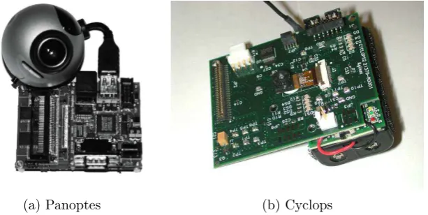
(a) Panoptes (b) Cyclops
Figure 2.2: Examples of WCN nodes present in the literature
interface, etc. A ChipCon CC2420 [25] implements the wireless interface
through the IEEE 802.15.4 standard. iMote2 can run TinyOS, embedded
Linux or University of California, Los Angeles’ SOS [39].
We would like to point out that the presented current consumptions have
been extracted from the datasheets of the chips. Measurement setups are
not known, except in some documents in which the manufacturer declares
that “all current consumption measurements are performed with all I/O
pins configured as inputs and with internal pull-ups enabled” [34]. As we
will see in Sec. 4.3, driving a pin of a peripheral requires lots of energy,
therefore the provided currents have to be considered as lower limits.
2.2
Related Work
2.2.1 Panoptes
The first significant example of a WCN node is Panoptes [40,4], first
devel-oped in 2003 by Fenget al. at the OGI School of Science and Engineering at
Oregon Health & Science University and then improved at the Department
of Computer Science of Portland State University. The first prototype is
MHz embedded processor [41], equipped with a Logitech 3000 USB-based
video camera, which applies some proprietary compression algorithm on
the acquired images, 64 Mbytes of memory, and an 802.11-based
network-ing card. The system runs the Linux 2.4.19 Operatnetwork-ing System (OS) kernel.
The entire system consumes approximately 5.5 W while capturing, com-pressing and delivering the stream of images acquired at 18− 20 frames
per second (fps) with a resolution of 320×240.
The authors moved to the Crossbow Stargate Platform [42] for the
sec-ond prototype. The Stargate Platform features a 400MHz, Intel PXA255
Processor, supported by an Intel StrongARM SA1111, 64 MB of RAM
and 32 MB of flash memory, from which the Linux 2.4.19 OS is loaded at
start-up. A daughter board mounted on the processor board provides USB
connectivity for the camera. In addition to being more powerful in terms
of processing capabilities with respect to the Bitsy Board, the Crossbow
Stargate Platform is also less power demanding (about 4 W).
From the point of view of the firmware, the authors developed a unit
for power management, and a set of blocks for capturing, filtering,
com-pressing and transmitting the images. The power manager is in charge of
determine the best acquisition and wireless transmission policy according
to the energy available, in compliance with the application. Video
cap-turing consists on decompressing the data coming from the USB interface
to allow image manipulation. Then, images are filtered to remove
redun-dant information, e.g. by detecting the only portions in the scene that has
changed with respect to the previous frame. The filtered images are then
compressed, e.g., with JPEG, to reduce the amount of power spent in the
transmission, and then sent to the wireless transceiver, which is in charge
of managing the available bandwidth by selecting the frames to the
trans-mitted according to a priority-based mechanism. The nodes communicate
in-formation for surveillance purposes.
The overall performance strongly depends on the specific
implementa-tion of the video capturing, filtering and compressing blocks. In particular,
the amount of processing load is strictly connected to the resolution of the
acquired images and the routines developed for image compression. The
authors analyzed the power consumed by one board in several
configura-tions (idle, camera on, camera and networking on, etc.), finding out that
1/3 of the power budget is spent for wireless transmission. In order to save power, the system switches components off or sets them to low power modes
whenever possible. In general, this approach partially solves the problem,
as on/off or wake/sleep transitions may require a substantial amount of
energy.
2.2.2 Cyclops
Another important example of WCN is Cyclops [5], an electronic interface
between a camera module and a standard WSN host mote. It was
devel-oped by Rahimi et al. at the Center for Embedded Networked Sensing,
UCLA, Los Angeles, CA, USA in conjunction with the Agilent Technology
Laboratories, in Palo Alto, CA, USA.
Cyclops consists on an Atmel ATmega128L MCU supported by a 64 KB
SRAM and 640 KB of flash memory. The MCU, based on an 8 bit RISC
architecture, is clocked at approximately 8 MHz and interfaces with a
352 × 288 CMOS imager through a CPLD, which is also responsible for
simple but fast image processing while receiving data. The combination of
CMOS imager, an ADCM-1700 from Agilent Technology [43], and a CPLD,
a Xilinx XC2C256 CoolRunner[44], brings several advantages. CMOS
im-agers are cheap and low-power, and at the same time they allow to perform
some control and processing directly on-chip. CPLDs are fast, overcoming
speeds, and power efficient, since negligible energy is consumed when their
clock source is disabled. This can be done as soon as they terminate their
tasks, without the need to turn them off completely. The MCU represents
the core of Cyclops: it is responsible for the management of the entire
node, selecting the power mode of the other elements, determining what
and when to transmit, and interfacing with the host mote. The CPLD
is used as interface between the sensor and the MCU itself, which is too
slow to cope with the sensor output data rate, and as a first level image
processor that operates while grabbing the image.
The firmware in Cyclops consists of a set of drivers required by the
MCU to communicate with the peripherals, a library to perform image
manipulation both at low (e.g., matrix operations) and high level (e.g.,
background subtraction), and a so called “Sensing Application” which
re-ceives commands from a host-PC and executes them, exploiting the
avail-able resources. Tested applications include a simple object detection
al-gorithm, based on background subtraction, and hand postures recognition
for human-computer interaction.
The joint use of a low-power device and of a fast one achieves a
signif-icant (one order of magnitude) improvement in terms of energy
require-ments with respect to Panoptes (the authors declare a power consumption
of less than 100 mW for Cyclops, to be added to the consumption of the
external sensor network host node), but it offers limited processing
capa-bilities and a low acquisition rate (only 5 fps, according to the imager’s
datasheet).
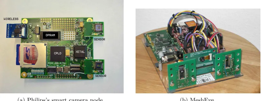
2.2.3 Philips Smart Camera Mote
Kleihorst et al., from the Philips Research Laboratories, Eindhoven, The
Netherlands, proposed a different solution in [6]. In order to minimize
to two VGA color image sensors, the node exploits a Massively-Parallel
Single-Instruction, Multiple-Data (MP-SIMD) processor, the Xetal-II [45].
The architecture of this processor consists on a linear processing array
with 320 processing elements supported by a 10 Mb on-chip memory to
buffer the image. Three further processor are present, managing the input
stream, the output stream and for global control respectively. Everything
is included in one sigle chip, which is clocked at 84 MHz. The rationale
behind this approach is that often, when processing an image, the same
calculations (e.g., convolution) are repeated on relatively small blocks of
neighboring pixels by sliding a “kernel” throughout the image. The SIMD
architecture exploits such intrinsic parallelism of images by elaborating all
the fetched data in parallel with the same instruction, thus providing a
very high throughput and low latency even with high resolution images
and complex image-processing algorithms. As an example, the authors
tested the processor with a 11 × 11 convolution on a 640 × 480 image,
requiring as little as 2 ms to execute. Power efficiency is achieved also,
since the mechanism reduces the number of accesses to the memory and
cuts down the overhead for control and address decoding. Nevertheless,
the absolute power consumption is high, with a peak value on the order
of several hundreds of milli-watts. With such requirements, it would not
be feasible for such a node to run on batteries continuously, acquiring
several frames per second. On the other side, the Xetal-II power efficiency
perfectly suits to camera-based WSNs, enabling many applications which
usually require a pc connected to the power outlet to run. In a multi-tier
network of wireless nodes, this node would lie near the highest tier.
2.2.4 MeshEye
Sensor diversity is the main characteristics of MeshEye [7], developed at
(a) Philips’s smart camera node (b) MeshEye
Figure 2.3: More examples of WCN nodes present in the literature
Hengstler and Aghajan. This node hosts up to eight (but two are
ac-tually used) low-power, low resolution, low color depth imagers and one
VGA camera. In particular, the ADNS-3060 optical mouse sensors [46]
(3030 pixel, 6-bit grayscale), and the ADCM-2700 CMOS camera module
[47](480640 pixel programmable, grayscale or 24-bit color) by Agilent
Tech-nologies are the ones present on the board. A high performance MCU, the
Atmel AT91SAM7S64 [48], represents the node core and is responsible for
both control and data processing. It incorporates an ARM7TDMI ARM
Thumb processor based on a power-efficient 32-bit RISC architecture that
can be clocked up to 55 MHz, a 16 KB SRAM and a 64 KB flash memory,
and is supported by an external MMC/SD 32 MB flash memory card for
temporary frame buffering/image archival. The acquisition policy consists
on performing acquisitions having only one low-power imager on, to
per-form basic motion detection, when the scene is static. If the node detects an
event, it turns on also the second low-power imager to perform stereo-vision
based 3D blob dimensioning and localization, and a high resolution image
is taken with the VGA camera. The output of the two low-power imagers
is used to determine the portion of the high resolution image in which the
data. Then, the ChipCon CC2420 2.4 GHz IEEE 802.15.4/ZigBee-ready RF transceiver allows wireless communication.
The authors claim that, when the frequency of events is low, the lifetime
of the node, powered with two AA batteries (2850 mAh), ranges between
ten and forty days, for an average current of 3 mA in the best case.
How-ever, the frame rate of the system is low (less than 2 fps]); increasing the
acquisition rate significantly reduces the lifetime of the node, with an
incre-ment in power consumption which is almost linear. Nevertheless, a frame
rate of at least 10 fps is often desirable, but such a high acquisition rate
would deplete the batteries in less than two days.
2.2.5 Yale’s AER imager-based node
All of the systems above acquire and process images at full resolution and
full pixel depth. This approach requires substantial memory to store the
images and powerful processing units to process them. A different approach
was taken by Teixeira et al. [9] at Yale University, New Haven, CT, USA.
Their work proposes a non-standard imager in which the concept of frame
is replaced by an Address Event Representation (AER). In practice, every
pixel is uniquely identified by an address and, instead of just measuring
the amount of light impinging on each pixel, it senses a precise property
of the scene, such as temporal and spatial difference. Every time the
mea-sured “amount” of such property exceeds a predefined threshold, the pixel
address is “fired”. The higher the frequency of firings associated to a pixel,
the greater the intensity of the phenomenon for that pixel. No image is
actually generated, at least not in the way we are used to: the concept of
frame is totally missing and the generated data are not directly readable
by humans. Nevertheless, this approach simplifies the detection of the
por-tions of the image in which most of the activity is taking place and might
significant amount of processing inside the sensor, therefore reducing the
overall processing and power requirements. As it will be discussed later in
Sec. 3.1.2, this is a crucial point in the development of low-power WCN
nodes.
With the data generated by this sensor, the authors were able to
de-velop applications for assisted living, including recognition of behaviors
of people in a house. Unfortunately, the sensor node is a standard,
high-performance iMote2, featuring an Intel XScale processor, operating at more
than 100 MHz, supported by a 32 MB SDRAM and a 32 MB flash
mem-ory. Such high processing capabilities have a critical impact on the power
requirements, which are in the order of hundreds of milli-watts. Moreover,
the previously described camera has not been really mounted on the mote,
but just simulated. In the end, it seems that no measurements on a real
prototype have been carried out to prove the effectiveness of the approach.
2.2.6 Other nodes
The previous list of research works does not include many other nodes
that have been proposed in this field. Our selection of works is focused
on power aspects rather then application development, networking or any
other issue. Here in the following we will briefly introduce other popular
nodes which, in our opinion, brought a marginal contribution, but still
important, in our field of investigation.
Cao et al. proposed a mote in [49] in which image acquisition, image processing and data compression are delegated to an FPGA, while sensor
control and RF module management are performed by an embedded 32-bit,
mem-ory and SDRAM are required to store the program and for data buffering.
As RF module, the ChipCon CC1000 has been chosen. Images are
pro-cessed with the aim of detecting unusual events, in which case the acquired
frame is compressed and transmitted. No power consumption analysis has
been provided, but according to the hardware equipment we can expect it
to be in the order of the watt.
WiSN nodes [51], where the “i” stands for “image”, presented by Downes, Rad and Aghajan from the Wireless Sensor Networks Lab of
Stan-ford University (CA, USA) are the very first example of nodes equipped
with heterogeneous imagers, and basically represent the embryonic form of
MeshEye, since they were developed in the same laboratory and are based
on the same processor (please refer to Sec. 2.2.4).
eCam [52] is an “ultra-compact, high data-rate wireless sensor node with a miniature camera”. Basically, it consists on a camera module
inte-grating a multi-resolution camera, the OmniVision OV7640 [53], attached
to the Eco Wireless Sensor platform [54], a tiny (' 1 cm3) host-node,
inte-grating a 2.4GHz RF transceiver with embedded 8051-compatible MCU2
and ADC, the NRF24E1 by Nordic Semiconductor [56], and 3-axial
ac-celeration, temperature and optical sensors. The node can interface with
other modules via a 16 pin expansion connector. The system processing
capabilities are very limited, no image processing is performed. All the
node can do is acquiring images and transmitting them. The low power
characteristics of the node do not seem to fit to camera-based sensor
net-works.
CMUcam3[57] is mainly oriented towards a simple programming inter-face, thanks to its open source framework and C programming. It consists
on an Omnivision camera module, either an OV6620 [58] or an OV7620 [59],
2“The 8051 is an 8 bit MCU originally developed by Intel in 1980. It is the world’s most popular
a NXP LPC2106 microcontroller [60], based on a 32 bit ARM7TDMI-S
pro-cessor, and a Fitst In, First Out (FIFO) memory chip for image buffering,
an Averlogic AL4V8M440 [61]. The presence of the FIFO significantly
re-duces the complexity of the system, but at the same time introre-duces an
important source of power consumption, which is in the order of several
hundreds of milli-watts for the entire node. CMUcam3 has been interfaced
with a Firefly platform [62] in [63] to achieve a complete WCN system.
The Firefly platform is a low-power custom node developed at Carnegie
Mellon University, Pittsburgh, PA, USA, which achieves a tight time
syn-chronization among nodes.
MicrelEye [64] consists of a hybrid architecture System on a Chip (SoC), the Atmel FPSLIC [65], which contains a low power MCU and an
FPGA. A CMOS sensor, 1MB of external SRAM and a Bluetooth
mod-ule complete the mote hardware configuration. The tasks delegated to the
MCU include sensor configuration and part of the object recognition
algo-rithm, while the FPGA performs image capturing, SRAM access and
Blue-tooth management, image processing and the top level control through a
finite state machine. As software application, an Support Vector
Machine-based object-detector has been developed. Power consumption is in the
order of hundreds of milli-watts.
Citric [8] is a daughter board of a Tmote Sky host-node. It integrates an OmniVision OV9655 [66], a low power, multi-resolution (from 40×30,
up to 1280 ×1024 pixels) CMOS camera module with image processing
capabilities, and a Marvell PXA270 embedded processor connected to a
64 MB SDRAM and a 16 MB FLASH for image buffering and code storage
respectively. A microphone is present too. Developed applications include
image compression, target tracking and camera localization. Due to the
In this section we have listed the WCN nodes proposed by researchers
in the past years: most of them offer good processing power, but they
run algorithms on images provided by high resolution, high color depth
sensors. Therefore, the latency delays introduced by image processing and
the power consumed by the entire node are often so high that the “low
power” characteristics are achieved only by reducing the frame rate to one
or two frames per second.
This general condition conflicts with the requirements set by
applica-tions in the fields of security, automotive, animal monitoring, etc., where
the dynamics of the monitored objects is much faster than a second.
Con-sider for example an application in which we want to monitor the speed
of cars on a highway. At the speed of 130 km/h, cars cover more than 36
meters in a second. Many frames are required in order to provide a reliable
measure. At low frame rates, we would need to place the node far away
from the scene to have a view wide enough to take several snapshots of
the same object with the same camera. This may not be feasible and in
general is not desirable.
We think that most of the previously described nodes would fit
through-out the tiers of a multi-tier WCN, but none of them could occupy the lowest
tier, meaning that the whole network would not be able to survive for a
long period of time. Even MeshEye nodes (presented in Sec. 2.2.4), which
try to overcome the problem exploiting both low- and high-resolution
im-agers, do not succeed in achieving a long lifetime. In fact, the presence of
a high performance MCU, which is required to process the high-resolution
images, reduces the advantages brought by the presence of low-resolution
cameras.
There is the need for ultra-low-power nodes that monitor the scene
continuously at high frame rate, even in a coarse way, looking for events of
in particular circumstances. This would guarantee a better usage of the
energy resources, increasing the network lifetime by one, even two orders
of magnitude. Moreover, it would allow even to more powerful nodes to
take part to the system. Within the previous example, the task of the
nodes belonging to the lowest tier would consist on detecting the presence
of cars and possibly determining a rough estimate of their speed. They
would then activate the higher tiers only when they discover the presence
of a fast car. In practice, they would act as a filter that cancels all the
Designing an Ultra-Low-Power WCN
Node
There are several problems underlying the design process of an
ultra-low-power WCN node. We will analyze these problems and suggest a design
method that leads to a node that can work for months powered with a
cou-ple of standard batteries. This chapter is organized as follows. In Sec. 3.1
we will identify the logic elements that make up a WCN node and we will
summarize the characteristics that the hardware embodiments of such
el-ements need to have in order to achieve ultra-low power consumption. In
Sec.3.2 we will discuss about the firmware implementation, describing how
to manage the hardware resources to get the most out of our node, how
to exploit the low-power characteristics of the devices and when to use the
high-processing capabilities present on board. Finally, the power model
corresponding to such a design is described in Sec. 3.3.
3.1
Hardware
Within an embedded system we can always identify a set of logic elements
that make up the system, i.e., a set of entities with specific tasks to carry
will be used by some other entities. Each logic element provides its
con-tribution to accomplish the duty for which the entire system has been
de-signed for. This can be also seen in a hierarchical way, with logic elements
that are divided into smaller elements.
Each logic element has an hardware embodiment in which it is
imple-mented, a device that has been designed or programmed to carry out the
tasks assigned to the logic element itself. The association between logic
elements and hardware embodiment is not necessarily bijective: the
imple-mentation of a logic element could be split into several devices and, at the
same time, one single device may contain more than one logic element.
We conceive a WCN node as made up by four main logic components:
acontrol unit (CU), which manages the whole node, deciding when the other logic components need to be operative and coordinating their
activities, aiming at executing the node’s tasks spending the minimum
amount of power;
a sensor, seen as an entity that transforms the information present in the outside physical world into data that can be processed by a
computing system;
a memory, that acts both as a buffer where to store the data coming from the sensor, waiting to be processed, and as a place where to store
the processing results, which may be needed in the future;
aprocessing unit (PU), which runs algorithms on the acquired images, trying to reduce the amount of data to transmit as much as possible;
a transceiver (TRX), for wireless communication.
We will try now to identify the most suitable hardware embodiment for
3.1.1 Control unit
The CU’s job consists of several simple tasks such as providing timing
signals to the sensor, managing the data transfer from the sensor itself and
the memory, activating/disabling the PU, deciding when to enable wireless
transmission and reception. Such tasks do not typically require high timing
resolution and no high processing capabilities are required too, as long as
most of the processing is carried out by the PU. Therefore, the CU can be
implemented on an ultra-low-power device, clocked at a very low frequency
(low frequency clocks easily exceed the kilohertz, thus achieving a precision
smaller than 1µs, which is sufficient for most sensors). This is the case, for example, of low-power microcontrollers, as the Texas Instruments MSP430
Microcontroller, which is also present in the Tmote Sky and the TelosB
nodes (refer to Sec. 2.1.4). The availability of a well supported embedded
OS such TinyOS is also an important factor, since it provides facilities for
time synchronization among nodes, multi-hop routing, self-management of
the network, etc. An ultra-low-power PLD represents a second option:
it allows to design multiple Finite State Machines (FSMs) operating in
parallel, to disable portions of the system by simply AND-gating their
clock and to employ multiple clock domains. When needed, it can also
generate high accuracy timing signals with a high frequency clock that is
fed to a small portion of the internal logic, with a limited effect on the
overall power consumption.
3.1.2 Imager
The choice of the imager has a strong impact on power consumption. The
higher the resolution and the color depth, the higher is the amount of data
to transfer, buffer, and process. The activity on input and output pins
if the hardware unit responsible for processing does not provide enough
memory to buffer the entire image. In this case, another device such as
a FIFO memory has to be involved in the entire process. Therefore, the
designer should select the imager that provides enough, but not more visual
information than necessary to run the algorithms.
Although standard imagers are mere light sensors, it may be convenient
to use a device that senses specific visual properties of the scene, such as
local contrast, image texture, or motion. We will call such device a “vision
sensor”, as opposite to image sensors. This approach can reduce the power
consumption of the overall node. First of all, the chip generates less data,
thus limiting signal activity and required memory size. Performing
opera-tions on-chip rather than on an external component is also power-efficient.
Processing is inherently parallel, with the same local operator replicated at
each pixel. By performing the initial (and often most computationally
in-tense) operations at the sensor level, subsequent (and more power hungry)
processors only need to deal with selected frames and image areas, with
positive impact in terms of latency, device occupancy and system
com-plexity. For instance, suppose that the application requires to enhance the
edges of the acquired image. Assuming a resolution of 128×64 with 8 bpp,
we have to transfer and buffer 64 Kb of data. Then, edges can be extracted
sliding a 3 ×3 mask throughout the image. This operation requires, for
each pixel, 9 multiplications, 8 additions and 1 division. Thresholding may
be used to reduce the amount of data down to 8 Kb, too. Performing such
operations on a processor running at 10 MHz, assuming only 1 clock cycle
per operation, introduces a latency of 15 ms. Clearly, such memory and
processing requirements are not suitable for an ultra-low-power system. On
the other side, a custom imager can achieve the same goal by performing
the processing task in the analog domain or in the in-pixel digital circuitry,
is reduced by a factor of 8, no latency is introduced and the requirements in
terms of processing capabilities can be relaxed. This comes at the expense
of a more complex sensor design process.
If most of the initial processing is performed at the sensor level, the
sensor itself can communicate whether a frame contains relevant image
data to be further processed. For example, the sensor may produce the
number of “active” (interesting) pixels in a frame; accordingly, the CU
may then decide whether the image data should be further analyzed by
the PU or not. In the first case, we will say that the sensor is in Active
mode, which implies data transfer to the PU. In the second case, the sensor
is inIdle mode, and no data needs to be transferred. Note that, even when
in Idle mode, the sensor still acquires and processes the image, although
data is not transferred to the PU.
In other words, vision sensors merge the sensing unit with part of the
processing unit, moving portions of the whole computation closer to where
data are generated. This turns to be very efficient especially in case of
mask filters, that operate on small groups of neighboring pixels and thus
allow to exploit the spatial proximity of the sensor’s photodiodes. This
helps to save time and energy with respect to a processor which needs to
fetch data located far away in the memory.
3.1.3 Memory
A memory unit is required every time the processing unit is not able to
process the data right away as they become available at the sensor output
pins. This situation occurs most of the times, e.g., when we have no
complete control over the readout process, as in the case in which the
sensor provides output data in a single burst after a “start” trigger. Or
we may need to compare two images, for motion detection or background
algorithm on the same image. Again, we may decide to apply a filter on
the acquired image only in particular circumstances, according to some
parameter extracted from the image itself.
Mainly, the memory component must satisfy the requirements set by
the node in terms of size, speed and power consumption. As usual, these
parameters are conflicting. It is also important that Direct Memory Access
is supported when the burst of data runs at high speed. Other important
parameters include latency and interface modality.
In the light of these consideration, Static RAMs (SRAMs) seem to be
the right solution, since they are faster and consume less power with
re-spect to Dynamic RAMs (DRAMs), which also require data refresh. The
problem with SRAMs lies in their price, which is much higher due to the
higher number of transistors required per memory element, if compared
to DRAMs. Another possibility involves the use of soft memories
imple-mented in a PLD, which, by the way, are usually built on SRAM
tech-nology. This solution allows an easy interface and typically satisfies the
requirements in terms of speed imposed by the sensor. This is optimal
when the CU and/or the PU are implemented on the same PLD, since
system complexity is reduced. In addition, such an architecture allows to
reduce power consumption simply by disabling the soft-memory clock.
3.1.4 Processing unit
Unlike in standard WSNs, where the major source of power consumption
is represented by the only transceiver [67], in camera-based SNs the
contri-bution brought by the PU becomes as much as important. In fact, WCNs
combine the huge amount of data generated by the sensing unit with the
high acquisition rates imposed by the applications. Thus, the PU is
re-sponsible of reducing the entire stream of data to a single, short message
Moreover, this “information synthesis” task needs to be carried out in a
limited amount of time. Therefore, once the right sensor has been
iden-tified, the designer must choose the processing device that allows to meet
the two conflicting requirements set by the application: processing power
and power consumption.
The required processing capabilities depend on the complexity of the
al-gorithms to implement and the rate at which such alal-gorithms are executed.
Basically, the timetproc required for processing has to be much shorter than
the frame period tf rame. We say “much shorter” because we would like to
execute the algorithm in a fraction of the frame period, so that the PU
stays idle for most of the time. Once the algorithm has been designed, and
given the resolution (m×n) of the images provided by the sensor, the value for tproc depends on the clock frequency fclock and the architecture of the
PU itself. In fact, the same instruction can be executed in one clock cycle
by a processor and in several clock cycles by another processor. We can
measure the efficiency of a processor through the average number of
In-structions Per Cycle (IPC) that it performs while executing the algorithm.
Features such as hardware multipliers, availability of floating point
arith-metics and multitasking affect such parameter. From our point of view,
in order to take into account the complexity of the algorithm, we extract
the average number of clock cycles per pixel Ncpp required to process the
images, which is given by the IPC multiplied by the number of instructions
per pixel. In the end, it has to be that:
tproc =
(m×n)×Ncpp
fclock
tf rame. (3.1)
For instance, suppose we equip our node with a 128×64 camera that
acquires images at up to 30 fps, and suppose that the algorithm that we
output. Well, in this case, we would need a processor that can run at:
fclock
(m×n)×Ncpp
tf rame
' 24 MHz. (3.2)
By employing FPGAs instead of processors, we can significantly relax the
requirements. This is due to their intrinsic ability to process data in a
parallel and pipelined fashion, which allows to reduce the Ncpp parameter
by several factors.
Within the given set of devices which fulfill the requirements in terms
of computational capabilities, we need to find the one(s) that satisfies the
power requirement set by the application. Generally speaking, there are
two working modes that we need to take into account. The node can
either monitor the scene just looking for some event of interest to happen or
carefully analyze the full image when a potential event has been discovered.
In the former case, we will apply simple and fast algorithms, so that the PU
spends most of the time in a low-power mode. In the latter case, we need
to produce accurate results about the ongoing events, therefore we would
like to exploit the PU at its full potential. For each of these cases, we define
a selection criterion that applies to the power consumed in low-power and
active mode respectively, whose values are present on the datasheet of each
device. The constraints are given by the capacity C provided by the node’s power source and the minimum expected lifetime L.
Let’s first consider the low-power working mode and determine the
max-imum current ilow−power that is allowed by the constraints. Since the entire
network will succeed in achieving long lifetime only if the PU operates in
this mode in the great majority of the cases, and since we are just defining
“order-of-magnitude” requirements, we can assume that the node always
operates in low power mode. Thus, it has to be that:
C
ilow−power ≫