Volume 3, Issue 2, February 2014
Page 177
ABSTRACT
Gallium doped zinc oxide (GZO) thin film has been deposited by spray pyrolysis technique onto glass substrates. The Effect of annealing temperature on the structural, morphological and optical properties of Ga0.03Zn0.097O thin film has been investigated.
All the films are polycrystalline with a preferential c-axis (002) orientation. It is shown that the full width at half maximum (FWHM) value decreases from 0.4472 to 0.27170 with increasing annealing temperature indicating the improvement of the
crystalline quality of Ga0.03Zn0.097O film. The surface morphology changed with the varying annealing temperatures. It is
observed that, as the annealing temperature increased, the diffusion of atoms on the surface of glass substrate was enhanced, resulting in a flat or less rugged surface with (RMS) roughness 0.929 nm for the sample annealed at 450oC. Therefore it is concluded that the sufficient surface diffusion leads to the improvement of crystalline quality which accompanies the modification modification of the surface morphology. The as-deposited film was less transparent in the visible and IR regions than other annealed films and the transparency of the films improved as the annealing temperature increased up to 450oC and then it decreases for further increasing in annealing temperature at 500oC.
1. INTRODUCTION
ZnO is a II-VI semiconductor with a large band gap (approx. 3.4 eV) at room temperature and has large exciton binding energy (~60 meV) [1]. Wide-band gap oxide semiconductor for optical devices, liquid crystal displays, and solar cells have attracted much attention. ZnO has been a promising material for many different applications such as gas sensors [2], transparent electrodes [3], piezoelectric devices [4], varistors [5], and surface acoustic wave devices [6]. ZnO thin film is fabricated by several methods: sputtering [7], [8], reactive plasma deposition (RPD) [9], [10], pulsed laser deposition (PLD) [11], metal organic vapor phase epitaxy (MOVPE) [12] and spray pyrolysis [13], [14].
While synthesizing transparent conducting oxide (TCO) thin films, it is a common practice to introduce impurities such as In, Al, Ga, N, P, As and F [15], within ZnO thin films in order to enhance the optoelectronic properties. All the transparent conductive doped ZnO films provide excellent UV shielding due to the absorption edge on the short wavelength side (λ~300nm)[16]. Beside, high reflectance in the IR region can make this a good candidate for application as the coating for IR reflecting mirror or heat reflector, as well as in other field of technology [17], [18]. All these applications require films with good uniformity, high electrical conductivity and high electron concentration simultaneously with high transmittance to visible light and high reflectance to near-IR light [19], [20]. From many reported investigations of the doped effect of impurity on ZnO, Ga doped seems to be the most successful and promising due to its advantages, such as the similar atomic radius compared to Zn, which could result in only small lattice deformation even for the case of high Ga concentrations [21], [22]. Also, Ga is less reactive and more resistive to oxidation compared to Al [23], [24]. Therefore, Ga doping can produce higher electron concentration than Al doping, which may be more useful for improving the reflective behavior of transparent conductive ZnO films according to Drude theory.
In this study, we fabricated and characterized Ga0.03Zn0.097O single-layer film as the first step of the application mentioned above. Then, effect of annealing temperature on the several fundamental properties such as structural, morphological and optical properties of the obtained film has been investigated.
2. EXPERIMENTAL
The Ga0.03Zn0.097O thin film was deposited by spray pyrolysis technique under ambient atmosphere. Two kinds of aqueous solutions, Zinc acetate Zn(CH3COO)2.2H2O and Gallium nitrate Ga(NO3)2 ,were chosen as the sources of zinc and gallium respectively. The concentration of the solutions was kept at 0.1M and a few drops of HC1 were added to the solution to increase the solubility of the compounds. The Ga0.03Zn0.097O film was prepared onto ultrasonically cleaned glass substrate held at a substrate temperature of 350oC. The substrate temperature was maintained constant using temperature controller with an accuracy of ±10oC. The solution flow rate was fixed at 6ml/min. The samples were annealed under ambient atmosphere at 400, 450, 500 oC for 1hour.
The crystal structure of Ga0.03Zn0.097O thin films was investigated by X-ray diffraction (XRD) using SHIMADZU X-Ray diffractometer system (XRD - 6000). The surface morphology of Ga0.03Zn0.097O thin film has been examined by using atomic force microscopy (AFM, scanning probe microscope).The optical measurements of Ga0.03Zn0.097O thin film is
Physical properties of Ga
0.03
Zn
0.97
O thin film
prepared by spray pyrolysis: Dependence on
annealing temperature
Salam Amir Yousif1, Sana Juma Ali2
Volume 3, Issue 2, February 2014
Page 178
calculated from the transmittance and absorbance spectrum at normal incidence over the range (300 – 900 nm), by using UV-VIS spectrophotometer type (SHIMADZU) (UV-1600/1700 series).3.
RESULTS AND DISCUSSION
3.1. STRUCTURAL PROPERTIES
The crystal orientation and crystallinity of the film was determined by X-ray diffraction. Figure 1 shows the XRD spectra of Ga0.03Zn0.097O thin film as-deposited and annealed at 400, 450, 500
o
C under ambient atmosphere. At as-deposited and all annealing temperature the films are polycrystalline with a preferential c-axis (002) orientation along with the other (101), (100) reflections that corresponding to the hexagonal wurtzite structure of ZnO. This is because the similar radii between the Zn2+ ions and Ga3+ ions enable the substitution of Ga for Zn without any significant change in the lattice constants of Ga0.03Zn0.097O compared to those in ZnO. The observed d-values are presented in Table 1, and compared with the standard ones from the (JCPDS) data file (36-1451) [25]. This fact also indicates no change of the wurtzite structure, well-consist with other reports [26]-[30].
It is shown that the full width at half maximum (FWHM) value decreases from 0.4472 to 0.27170 with increasing annealing temperature indicating the improvement of the crystalline quality of Ga0.03Zn0.097O film. The crystalline quality of the films depends strongly on the annealing temperature due to the enhanced surface diffusion that comes with increasing annealing temperature, which is consist with the report [31].
Figure 1 XRD pattern of Ga0.03Zn0.097O thin film for different annealing temperature
Table1: XRD parameters of as-deposited and annealed Ga0.03Zn0.097O thin film Annealing Temperature deposited as- 400 450 500 JCPDS for
ZnO
(hkl)
(100)
2θ(deg.) 31.739 31.742 31.751 31.753 31.77 d(Ǻ) 2.8169 2.8167 2.8159 2.8157 2.816
Int. 58 56 40 40 57
(002)
2θ(deg.) 34.437 34.455 34.482 34.485 34.422 d(Ǻ) 2.6021 2.6008 2.5989 2.5986 2.602
Int. 100 100 100 100 44
(101)
2θ(deg.) 36.214 36.214 36.241 36.242 36.253 d(Ǻ) 2.4784 2.4784 2.4766 2.4766 2.476
Int. 88 84 67 65 100
The unit cell parameter (a, c) and the ratio of (c/a) belong to the (002) plane as a preferred orientation of Ga0.03Zn0.097O thin films deposited on glass substrate have been calculated using equation (1) [32]. The calculated values of lattice parameter (a, c) and (c/a) are shown in Figures 2,3 and listed in Table 2, found to be in a good agreement with the standard (JCPDS) values [25].
2 2
2 2 2
2 C
l
3a k hk 4h
d 1
Volume 3, Issue 2, February 2014
Page 179
Table 2: Lattice constants of Ga0.03Zn0.097O thin film
c/a c (Å)
a (Å) annealing temperature
1.5999 5.20434
3.25273 as-deposited (350)
1.5993 5.20172
3.25247 400
1.5985 5.19786
3.25157 450
1.5984 5.19728
3.25137 500
1.6021 5.20661
3.24982 (JCPDS)
Figure 2 a-axis lengths vs. annealing temperature
Figure 3 c-axis length vs. annealing temperature
Volume 3, Issue 2, February 2014
Page 180
inversely proportional with the full width at half maximum. The values of crystallite size of Ga0.03Zn0.097O thin films are shown in Figure 4, and listed in Table 3.
cos
.
D 09 (2)
Where λ is the wavelength of X-ray used (1.5406 Å), β is the full-width at half maximum (FWHM) of the peak which has maximum intensity and θ is the Bragg angle.
Figure 4 Crystallite size vs. annealing temperature
The texture coefficient (Tc) evaluated from equation (3) [33] is used to describe the preferred orientation of
Ga0.03Zn0.097O thin films. It is clear that the deviation of the texture coefficient from unity implies the preferred orientation of growth. The larger the texture coefficient deviates from unity, the higher will be the preferred orientation of
Ga0.03Zn0.097O thin films. The variation of texture coefficient estimated along (002) direction with annealing temperature of Ga0.03Zn0.097O film is shown in Figure 5. It was found that the value of texture coefficient increases with increasing annealing temperature as shown in Table 3.
(hkl) /I N
(hkl) I(hkl)/I (hkl)
T
o kl) I( 1 r
o
C h
(3)
Figure 5 Texture coefficients vs. annealing temperature
Volume 3, Issue 2, February 2014
Page 181
X100% C C C ε ASTM XRD ASTM (4)
The dislocation density(), defined as the length of dislocation lines per unit volume, has been estimated using the following equation [35], [36].
2 1
D
(5)
To derive the film stress (σfilm) parallel to the film surface, the following formula is used, which is valid for a hexagonal lattice [37]. bulk bulk film 13 12 11 33 2 13 film
c
c
c
2c
)
c
(c
c
2c
σ
(6)For the elastic constants cij, the following values for single crystal ZnO are used, C11 = 208.8 GPa, C33 = 213.8 GPa, C12 = 119.7 GPa, C13 = 104.2 GPa, Where: cfilm and cbulk are the lattice constants (c) of ZnO film and bulk (or powder).
Table 3: Structural properties of Ga0.03Zn0.097O film for different annealing temperature Annealing temperature Crystallite Size (nm) Texture Coefficient TC Micro Strain ε % Dislocation Density
(δ) stress Flim
(GPa)
asـdeposited
350 18.6 (101) (100) (002) 0.043 2.890 0.1001
400 21.8 0.633 0.731 1.63 0.093 2.104 0.2165
450 28.2 0.615 0.719 1.66 0.168 1.257 0.3911
500 30.6 0.551 0.577 1.87 0.179 1.067 0.4167
3.2. MORPHOLOGY
Figure 6 shows the AFM images of Ga0.03Zn0.097O samples as-deposited and annealed at 400, 450, 500 o
C . As shown in the figure, the surface morphology changed with the varying annealing temperatures. For the as-deposited film the surface morphology was rough and rugged, and the root mean square (RMS) roughness of this film was 1.29 nm. This is attributed to the fact that the surface diffusion was insufficient due to the low deposition temperature [38].However, after annealing the film at 400, 450, 500 oC under ambient atmosphere, the rough of the surface decreases with increasing annealing temperature up to 450oC and then it is increased for 500oC. The root mean square and grain size of
Ga0.03Zn0.097O as-deposited and annealed have been listed in Table 4.
It is observed that, as the annealing temperature increased; the diffusion of atoms on the surface of glass substrate was enhanced, resulting in a flat or less rugged surface with (RMS) roughness 0.929 nm for the sample annealed at 450oC. Therefore it is concluded that the sufficient surface diffusion leads to the improvement of crystalline quality which accompanies the modification of the surface morphology.
Table 4: RMS roughness, Grain size and peak-peak height of Ga0.03Zn0.097O film annealing temperature
RMS roughness (nm) Grain size (nm) Peak-Peak height (nm)
as-deposited 350 1.29 134.19 12.1
400 1.23 104.61 8.74
450 0.929 78.78 4.4
Volume 3, Issue 2, February 2014
Page 182
Volume 3, Issue 2, February 2014
Page 183
3.3. OPTICAL PROPERTIES
Figure 7 shows the optical transmittance spectra taken at room temperature. The annealed Ga0.03Zn0.097O films were highly transparent in the visible and IR regions from 400 to 900 nm and showed sharp absorption edge in the UV region. For the as-deposited film the transmittance is low compare with those of annealed films and no sharp absorption edge observed in this film. This indicates that the substrate temperature 350oC is not sufficient to arrange Ga and Zn ions sites in the lattice. We suggest that the band gap shift are directly proportional to the Ga ions which are substituted for the Zn ions in the film without changing the wurtzite structure, and at low deposition temperature, it is though that the Ga atoms are not incorporated in the ZnO lattice and are partially located at defect sites such as interstitials in Ga0.03Zn0.097O lattice. Furthermore, the as-deposited film was less transparent in the visible and IR regions than other annealed films and the transparency of the films improved as the annealing temperature increased up to 450oC and then it decreases for further increasing in annealing temperature at 500oC. The decrease in the transmittance for the film annealed at 500oC can be described to the decreasing Ga content as a result of the increasing of re-evaporation rate of Ga atoms from the
Ga0.03Zn0.097O film [31].
Figure 7 Transmittance spectra of Ga0.03Zn0.097O film at different annealing temperature
The absorbance spectra of the Ga0.03Zn0.097O thin film deposited on glass substrate at as-deposited and different annealing temperature that measured at room temperature is shown in Figure 8. In the high energy spectral range, where the film is strongly absorbent, and the absorbance of Ga0.03Zn0.097O films decrease with increasing of annealing temperature from, 350℃(as-deposited) to 450℃, then it goes on increases with increasing substrate temperature from 450℃ to 500℃.
Figure 8 Absorbance spectra of Ga0.03Zn0.097O film at different annealing temperature
Volume 3, Issue 2, February 2014
Page 184
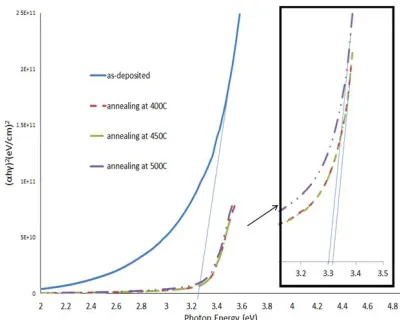
Figure 9 Variation of
(
h
)
2 vs. photon energy(
h
)
of Ga0.03Zn0.097O thin filmThe values of direct band gap are estimated from the extrapolated of the linear portion of the curve to zero absorption and found to be (3.25, 3.32, 3.32, 3.3) eV for the as-deposited and annealed Ga0.03Zn0.097O film at 400,450,500oC respectively, which are in agreement with the report [27] . From Figure 9 we can see that the bandgap of Ga0.03Zn0.097O thin film increases with increasing annealing temperature from (3.25 eV) at as-deposited 350℃ to (3.32 eV) at annealing temperatures 400, 450 ℃ and, then it decreases with increasing annealing temperatures from (3.32 eV) to (3.3 eV) at annealing temperatures 500℃.
4. CONCLUSION
Ga0.03Zn0.097O thin films have been deposited successfully onto glass substrates at 350 oCby spray pyrolysis technique. The full width at half maximum (FWHM) value decreases from 0.4472 to 0.27170 with increasing annealing temperature indicating the improvement of the crystalline quality of Ga0.03Zn0.097O film. The crystalline quality of the films depends strongly on the annealing temperature due to the enhanced surface diffusion that comes with increasing annealing temperature.
The surface morphology changed with the varying annealing temperatures. The surface morphology of as-deposited film was rough and rugged because the surface diffusion was insufficient due to the low deposition temperature. However, after annealing the film, the rough of the surface decreases with increasing annealing temperature up to 450 oC and then it is increased at 500 oC. As the annealing temperature increased, the diffusion of atoms on the surface of glass substrate was enhanced, resulting in a flat or less rugged surface with (RMS) roughness 0.929 nm for the sample annealed at 450oC. Therefore it is concluded that the sufficient surface diffusion leads to the improvement of crystalline quality which accompanies the modification of the surface morphology.
For the as-deposited film the transmittance is low compare with those of annealed films and no sharp absorption edge observed in this film. This indicates that the substrate temperature 350 oC is not sufficient to arrange Ga and Zn ions sites in the lattice. At low deposition temperature, it is though that the Ga atoms are not incorporated in the ZnO lattice and are partially located at defect sites such as interstitials in Ga0.03Zn0.097O lattice. Furthermore, the as-deposited film was less transparent in the visible and IR regions than other annealed films and the transparency of the films improved as the annealing temperature increased up to 450 oC and then it decreases for further increasing in annealing temperature at 500 oC. The decrease in the transmittance for the film annealed a 500 oC can be described to the decreasing Ga content as a result of the increasing of re-evaporation rate of Ga atoms from the film.
References
[1] K. Postava, H. Sueki, M. Aoyama, T. Yamaguchi, C. Ino, Y. Igasaki, M. Morie, J. Appl. Phys. 87 (2000) 7820.
[2] C. Kwon, H. Hong, D. Yun, K. Lee, S. Kim, Y. Roh, B. Lee, Sens. Actuators B. 25 (1995) 610.
[3] S. Major, S. Kumar, M. Bhatnagar, K. Chopra, Appl. Phys. Let. 49 (1986) 394.
[4] M. Ambia, M. Islam, M. Hakim, J. Mater. Sci. 27 (1992) 5169.
[5] K. Mukae, K. Tsuda, I. Nagasawa, Jpn. J. Appl. Phys. 16 (1977) 1361.
[6] S. Chang, Y. Su, Y. Shei, J. Vac. Sci. Technol. A 13 (1995) 385.
[7] T. Minami, T. Miyata, Y. Ohtani, T. Kuboi, Phys. Stat. Sol. (RRL) 1 (2007) R31.
[8] R. Cebulla, R. Wendt, K. Ellmer, J. Appl. Phys. 83 (1998) 1087.
[9] K. Iwata, T. Sakemi, A. Yamada, P. Fons, K. Awai, T. Yamamoto, S. Shirakata, K. Matsubara, H. Tampo, K. Sakurai, S. Niki, Thin Solid Films 480-481 (2005) 199.
Volume 3, Issue 2, February 2014
Page 185
[11]A. Agura, A. Suzuki, T. Matsushita, T. Aoki, M. Okuda, Thin Solid Films 445 (2003) 236.
[12]J. Steinhauser, S. Fay, N. Oliveira, E. Vallat-Sauvain, C. Ballif, Appl. Phys. Let. 90 (2007) 142107.
[13]A. Reddy, P. Prathap, Y. Subbaiah, K. Reddy, J. Yi, Thin Solid Films 516 (2008) 7084-7087.
[14]S. A. Yousif, A. A. Rasheed, N. F. Habubi, Journal of Electron Devices, 16(2012), 1347-1355
[15]S. J. Pearton, D. P. Norton,K.Ip, W.Y. Heo, T. Steine , Prog. Mater.Sci. 50 (2005) 293.
[16]Q. B. Ma, Z. Z.Ye, H. P. He, L. P. Zhu, J. R.Wang B. H. Zhao, Mater.Lett.61 (2007) 2460.
[17]G. Frank, E. Kauer, H. Kostlin, Thin Solid Films 77 (1981) 107.
[18]Q. B. Ma, Z. Z.Ye, H. P. He, L. P. Zhu, J. Y. Huang, Y. Z. Zhang, B. H. Zhao, Scr. Mater 58 (2008) 21.
[19]F. Q. Adurodija, H. Izumi, T. Ishihara, H. Yoshioka, H. Matsui, M. Motoyama, Jpn. J. Appl. 38 (1999) 2710.
[20]R. Das, S. Ray, J. Phys. D: Appl. Phys. 36 (2003) 152.
[21]S. J. Henley, M. N. R. Ashfold, D. Cherns, Surf. Coat.Technol. 177 (2004) 271.
[22]Q. B. Ma, Z. Z.Ye, H. P. He, S. S. Hu, J. R. Wang, L. P. Zhu, Y. Z. Zhang, B. H. Zhao, J. Cryst. Growth.304 (2007) 64.
[23]V. Assuncao, E. Fortunato, A. Marques, H.Aguas, I. Ferreira, M. E. V. Costa, R. Martins, Thin Solid Films 427 (2003) 401.
[24]Q. B. Ma, Z. Z. Ye, H. P. He, L. P. Zhu, Y. Z. Zhang, B. H. Zhao, J. Inorg. Mater.22 (2007) 1113.
[25]Joint Committee on Powder Diffraction Standards, Powder DiffractionFile, International Center for Diffraction Data, Swarthmore,PA(1997) card 36-1451
[26]W.T. Yen, Y.C. Lin, P.C. Yao, J.H. Ke, Y.L. Chen, Thin Solid Films xxx (2009) xxx–xxx
[27]A.R. Babar, P. R.Deshamukh, R. J.Deokate, D.Haranath, C. H.Bhosale, K. Y.Rajpure, J. Phys. D: Appl. Phys. 41 (2008) 135404 (6pp).
[28]A. Ohtomo, M. Kawasaki, T. Koida, K. Masubuchi, H. Koinuma, Y. Sakurai, Y. Yoshida, T. Yasuda, Y. Segawa, Appl. Phys. Lett. 72 (1998) 2466.
[29]W. Park, G. Yi, H. Jang, Appl. Phys. Lett. 79 (2001) 2022.
[30]T. Minemoto, T. Negami, S. Nishiwaki, H. Takakura, Y. Hamakawa, Thin Solid Films 372 (2000) 173.
[31]D. Hwang, M. Jeong, J. Myoung, Appl. Surf. Sci. 225 (2004) 217-222.
[32]A. Goswami, Thin Film Fundamentals, New Age International (P) Ltd. Publishers, New Delhi, (2005) 69.
[33]S. A. Yousif, J. M. Abass, International Letters of Chemistry, Physics and Astronomy13(2013) 90-102.
[34]T. Obata , K. Komeda , T. Nakao , H. Ueba , and C. Tasygama , J. Appl. Phys. , 81 , (1997) , 199 .
[35]V.Bilgin, S.Kose, F.Atay, I.Akyuz, Mater.Chem. Phys. 94 (2005) 103.
[36]S. Prabahar, M. Dhanam, J. Cryst. Growth 285 (2005) 41.
[37]R. Hong, J. Huang, H. He, Z. Fan, J. Shao, Appl. Surf. Sci. 242 (2005) 346-352.