Please cite this article as: A. Goudarzian, A. Khosravi, Voltage Regulation of a Negative Output Luo Converter Using a PD-PI Type Sliding Mode Current Controller, International Journal of Engineering (IJE), IJE TRANSACTIONS B: Applications Vol. 32, No. 2, (February 2019) 277-285
International Journal of Engineering
J o u r n a l H o m e p a g e : w w w . i j e . i rVoltage Regulation of a Negative Output Luo Converter Using a PD-PI Type Sliding
Mode Current Controller
A. Goudarzian*, A. Khosravi
Department of Electrical Engineering, Faculty of Engineering, Shahrekord Branch, Islamic Azad University, Shahrekord, Iran
P A P E R I N F O
Paper history:
Received 19 September 2018
Received in revised form 19 November 2017 Accepted 03 Januray 2019
Keywords:
Switching Converter
Negative Output Luo Converter PD-PI Type Sliding Surface Control Design
A B S T R A C T
This paper describes a new design for direct sliding mode method with a high switching frequency using the PD-PI type sliding surface applied to a negative output Luo converter worked in continuous current mode for applications required constant power source such as aerospace applications, medical equipment and etc. Because of the output power and line changes, the converter model is also nonlinear and time varying. In addition, losses dissipation and voltage drops caused a deviation between the theoretical and actual output voltage of this converter. For improvement of the converter performance along with the current and voltage regulations, a nonlinear controller is required. This suggested controller is proper to inherently variable structure of the converter and can cope with nonlinearities associated with its model. The goal is to ensure a satisfactory response for the converter. The practical results showed that the proposed strategy helps to eliminate the voltage error along with continuous current operation of the converter in very light loads and high switching frequency in different operating points.
doi: 10.5829/ije.2019.32.02b.13
1. INTRODUCTION1
In recent years, power converters are commonly employed in power supplies and industrial applications [1]. Theoretically, conventional topologies such as buck-boost, Sepic, Zeta, Cuk could be employed for voltage increment. However, effects of switches, diodes, and the consequence of resistances of passive elements and losses limit the practical voltage gain of the aforementioned converters. Moreover, duty ratio of the converters will tremendously increase by increment of the output voltage. This terribly large duty ratio leads to relatively high switching losses and severe reverse recovery crisis [2]. In two last decades, the voltage lift method has been well applied for design of power converters [3]. In addition, the super lift technique geometrically enhances the voltage gain, whereas the negative output Luo converter (NOLC) does the same operation. NOLC has a high voltage gain, high power density and high efficiency. For similar conditions, the switching stress of this converter is less than the
*Corresponding Author Email: [email protected] (A. Goudarzian)
switching stress of other conventional converters. It is an extremely useful feature to reduce switching losses. Hence, NOLC is used for this study. In practice, the voltage gain of a NOLC is dependent to parametric resistances of power circuit components and operating point. Hence, a controller is needed for adjustment of the magnitude of the output voltage with respect to its reference signal and guarantee the converter stability. From control viewpoint, the boost converters have a minimum phase and time-varying structure. The non-minimum phase converters have a slow dynamical response and small stability margins [4]. Hence, control of a NOLC is more complicated compared with minimum phase systems.
stability of converters. It may challenge the quality, performance and stability of power systems. Therefore, a voltage regulator is required. Peak current mode method (PCM) is a type of nonlinear methods which is designed for converters [7]. However, the problem of PCM is presence of an exterior ramp signal. Consequently, the current cannot exactly reach to its desired level. An adaptive backstepping controller is proposes for a POESLLC by Abjadi et al.[8]. However, this controller needs to precise knowledge of all parameters of the converter, excepting load. Therefore, the cost increases and productivity is reduced. Also, stability analysis and construction of fuzzy controllers are reported for converters, aiming to enhance large signal characteristics [9]. However, there is no systematic method for selection of coefficients of fuzzy controllers.
In the last decade, sliding mode controller (SMC) has been widely regarded for variable structure systems [10, 11]. Two major methods exist to implement an SMC for a switching power converter, namely the indirect and direct SMC techniques. In indirect method, the control law of a converter is obtained using the equivalent control concept [12]. However, the designed sliding variable is not bounded and the system response will be deteriorated. In direct method, the switching function is directly achieved using instantaneous trajectories of the SMC. One method to generate the pulse signals for the converter is to modulate the sliding plane within a parabolic modulator (PM) with variable bandwidth [13] or a constant bandwidth hysteresis modulator (HM) [14]. However, the proposed approaches in literature [13, 14] are used for minimum phase systems. For stabilization of a non-minimum phase converter, sliding mode current control (SMCC) method should be utilized. Mamarelis et al. [15] proposes a simple SMCC for boost and Sepic converters. Although the main objective is the voltage regulation, but any output feedback was not applied to generate the reference input current. So they are weak against large load uncertainties. Furthermore, switching frequency of power electronics systems with traditional direct SMCC will be constrained, due to time delays of command circuits, analogue to analogue conversions for isolated sensors and also, parametric resistances effects of power circuits, limited bandwidth of analogue devices and etc. For power converters, low switching frequency leads to inductor core saturation, noise, large voltage ripple and etc. In addition, implementation of a simple SMCC is proposed in literature [16, 17] using digital processors. However, digital control has a serious drawbacks, which decreases sampling frequency. By observing the reported data in literature [16, 17], it is found that the converter frequency is about 10 𝐾𝐻𝑧 for all the tests, provided by the authors. However, the frequency must be larger than the audible frequency i.e.
𝑓𝑆> 20 𝐾𝐻𝑧. It is recommended for low power
converters to work in interval of [20 200] 𝐾𝐻𝑧.
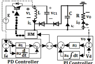
In view of the aforementioned discussions, this research presents a new direct SMCC controller via PD-PI type sliding surface. This solution can resolve the problems discussed in the above associated literature [11-17]. The proposed structure is presented in Figure 1. It is consisted of two loops; i) an inner loop through a proportional-integral (PI) controller. It is used to adjust the voltage and alleviate the voltage error, and ii) an outer loop via a proportional-derivative (PD) controller. It should be used for stabilizing the converter dynamics, minimizing inrush current and enhancing the switching frequency. By employing a PD compensator in the SMCC, derivative of the sliding variable (S) will be dependent to the impulse function. Therefore, the sliding surface derivative will be converged to infinite and high switching frequency operation will be achieved, despite of having a practical large hysteresis bandwidth. Other features of the controller, such as the steady state and dynamic performances are investigated in the paper. Theoretically, it is demonstrated that the utilization of a PD controller effectively enhances the switching frequency and practical tests are performed to confirm the validity of the suggested method
The contents of the paper are as follows. In section 2, a comparison between NOLC and other converters is preformed. design, development and system stability of the proposed PD-PI SMCC for a NOLC are investigated in section 3. The practical results are represented in section 4 and the conclusions are shown in section 5.
2. COMPARISON BETWEEN NOLC AND OTHER CONVERTERS
The NOLC diagram illustrated in Figure 1, and it consists of a semiconductor switch, two diodes, three energy storage elements, resistance and input source. The converter operation investigated in two mode. At the first mode, the switch and diode D1 are turned on and the
diode D2 is off. At the second mode, switch and diode D1
are turned off and diode D2 conducts. The advantages of
NOLC compared with other converters is expressed in the following expression.
The switching stress is defined as follows:
𝑃𝑆= 𝑉𝑇𝐼𝑇 (1)
where PS is switching losses, VT is switch voltage drop in
ON and OFF instants and IT is switch current in ON and
OFF instants. VT and IT are obtained for NOLC as
follows:
𝑉𝑇= v𝑂 (2-a)
𝐼𝑇= 𝐼𝑖𝑛= 𝑃𝑂
𝐸 (2-b)
where Δv𝐶1 is the voltage ripple of the middle capacitor and 𝑃𝑂 is output power. By using Equations (1) and (2), the switching losses of the NOLC can be given as follows:
𝑃𝑆= 𝑉𝑂
𝐸𝑃𝑂= 𝐺𝑃𝑂 (3)
where 𝐺 = 𝑉𝑂/𝐸 is the voltage gain. Similarly, the switching stress of buck-boost (BB), Cuk, SEPIC and Zeta converters can be determined as follows:
𝑃𝑆= (𝐺 + 1)𝑃𝑂 for BB, Cuk, SEPIC and Zeta (4) Comparing the switching stress of NOLC as expressed in Equation (3) with Equation (4). It shows that the switching stress of BB, Zeta, Cuk and SEPIC converters extremely increases in high voltage gains. But, the switching losses of the NOLC is less than others despite of increment of the voltage gain, resulting in low switching losses and high efficiency of the NOLC.
2. SMCC DESIGN
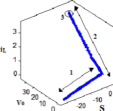
2. 1. Principles The operation of a SMCC depicted in Figure 2 for a NOLC. It provides a three-dimensional phase portrait for the inductor current iL, output voltage
vO and sliding variable S. For any initial operating
condition that the sliding variable doesn’t start from zero, the state trajectory of the sliding plane is constituted by three regions; namely, the reaching mode, the sliding mode, and the steady mode. In the first region, the state variables are enforced to approach to the sliding variable from any initial conditions. As soon as the sliding surface touches the origin, the state space variables of the converter slide along the sliding variable and approach to their equilibrium points in the second region. Finally, the phase trajectories of the sliding variable are maintained at zero, representing the steady region with no error. The operation of a perfect SMC needs an infinite switching frequency performance of the NOLC. However, in practical applications, the sliding motion of the phase trajectories often introduces the chattering problem at vicinity of the origin. For solving this problem, hysteresis modulation is proposed. However, this method reduces the switching frequency to a limited range.
Figure 2. The operation of a SMC. Line1: reaching trajectory; Line 2: sliding trajectory; Line 3: steady state region
Also, time delays restrict the frequency of a SMC. One suitable method to reduce the trajectory chattering is directly use of the PD-PI type of SMC within a constant hysteresis bandwidth.
2. 2. Closed Loop Analysis of the NOLC with the Proposed Pd-Pi SMC A PD-PI SMC for a non-minimum phase NOLC is depicted in Figurte 1. The reduced order averaging model of a NOLC in CCM can be determined as follows:
{
𝑑𝑖𝐿
𝑑𝑡= 𝐸 𝐿−
(1−𝑢)𝑣𝑂
𝐿 𝑑𝑣𝑂
𝑑𝑡 =
(1−𝑢)𝑖𝐿
𝐶 −
𝑣𝑂
𝑅𝐶
(5)
For NOLC, the voltage value of the middle capacitor equals to input voltage for all times. A second order PD-PI type of the sliding variable is chosen as follows:
𝑆 = 𝑎1𝑥1+ 𝑎2𝑥2+ 𝑎3𝑥3+ 𝑎4𝑥4= 𝑎1𝑒1+ 𝑎2𝑒1̇ +
𝑎3𝑒2+ 𝑎4∫ 𝑒2𝑑𝑡 (6)
where 𝑒1= 𝑖𝐿− 𝐼𝑑 and 𝑒2= 𝑣𝑂− 𝑉𝑑 are the current and voltage tracking errors, respectively. Also, a1, a2, a3 and
a4 are the parameters of the controller. For the converter,
the control law of the SMC is as follows:
𝑢 = {
1 𝑓𝑜𝑟 𝑆 < −𝜀 0 𝑓𝑜𝑟 𝑆 > 𝜀 𝑢𝑛𝑐ℎ𝑎𝑛𝑔𝑒𝑑 𝑓𝑜𝑟 − 𝜀 < 𝑆 < 𝜀
(7)
The sliding phase portrait of the controlled system is obtained as follows:
𝑎1𝑥1+ 𝑎2𝑥2+ 𝑎3𝑥3+ 𝑎4𝑥4= 0 (8)
Furthermore, 𝑒1̇, 𝑒1̈, 𝑒2, 𝑒2̇ can be derived as:
{ 𝑒1̇ =
𝐸 𝐿−
(1−𝑢)𝑣𝑂 𝐿
𝑒1̈ = 𝑢̇𝑣𝑂
𝐿 −
(1−𝑢)𝑣𝑂̇
𝐿
𝑒2= 𝑣𝑂− 𝑉𝑑
𝑒2̇ = 𝑣𝑂̇
(9)
u are the inductor current, output voltage, input voltage and switching state of the converter. u is 1 for ON mode and 0 for OFF mode. By using Equations (5)-(9), the time derivative of the designed sliding variable is obtained as follows:
𝑑𝑆
𝑑𝑡= 𝑘1𝐸 − 𝑘1(1 − 𝑢)𝑣𝑂+ 𝑘2𝑢′𝑣𝑂− 𝑘2(1 −
𝑢)𝑣𝑂′ + 𝑎3𝑣𝑂′ + 𝑎4(𝑣𝑂− 𝑉𝑑)
(10)
where
𝑘1=𝑎𝐿1, 𝑘2=𝑎𝐿2 (11)
For analysis of the system stability, the existence and stability conditions are checked. The first condition was investigated using a Lyapunov function. Let us define Equation (12) as a positive function for the described system:
𝐹 =1
2𝑆
2> 0 (12)
Differentiating Equation (12) gives:
𝐹′= 1
2𝐿𝑆(2𝑎1𝐸 − 2𝑎1(1 − 𝑢)𝑣𝑂+ 2𝑎2𝑢̇𝑣𝑂+
[2𝐿𝑎3− 2𝑎2(1 − 𝑢)] ( (1−𝑢)𝑖𝐿
𝐶 −
𝑣𝑂
𝑅𝐶) + 2𝐿𝑎4(𝑣𝑂−
𝑉𝑑))
(13)
when 𝑆 > 𝜀, switch is OFF (u=0, 𝑢̇ = −𝛿(𝑡)) and Equation (13) is simplified as follows:
𝐹′= 1
2𝐿𝑆(2𝑎1𝐸 − 2𝑎1𝑣𝑂− 2𝑎2𝑣𝑂𝛿(𝑡) +
[2𝐿𝑎3− 2𝑎2] (𝑖𝐶𝐿−𝑅𝐶𝑣𝑂) + 2𝐿𝑎4(𝑣𝑂− 𝑉𝑑))
(14)
when 𝑆 < −𝜀, switch is ON (u=1, 𝑢̇ = 𝛿(𝑡)) and Equation (13) is simplified as follows:
𝐹′= 1
2𝐿𝑆(2𝑎1𝐸 + 2𝑎2𝑣𝑂𝛿(𝑡) − 2𝐿𝑎3 𝑣𝑂
𝑅𝐶+
2𝐿𝑎4(𝑣𝑂− 𝑉𝑑))
(15)
By combining Equations (14) and (15), Equation (13) can be expressed as follows:
𝐹′= 1
2𝐿[𝑆 (2𝑎1𝐸 − 2𝐿𝑎3 𝑣𝑂
𝑅𝐶+ 2𝐿𝑎4(𝑣𝑂− 𝑉𝑑) −
𝑎1𝑣𝑂+ [𝐿𝑎3− 𝑎2] 𝑖𝐿
𝐶+ 𝑎2 𝑣𝑂
𝑅𝐶) − |𝑆| (𝑎1𝑣𝑂+
2𝑎2𝑣𝑂𝛿(𝑡) − [𝐿𝑎3− 𝑎2] 𝑖𝐿
𝐶− 𝑎2 𝑣𝑂
𝑅𝐶)]→ 𝐹 ′=
1
2𝐿|𝑆| [𝑠𝑔𝑛(𝑆) (2𝑎1𝐸 − 2𝐿𝑎3 𝑣𝑂
𝑅𝐶+ 2𝐿𝑎4(𝑣𝑂−
𝑉𝑑) − 𝑎1𝑣𝑂+ [𝐿𝑎3− 𝑎2] 𝑖𝐿
𝐶+ 𝑎2 𝑣𝑂
𝑅𝐶) − (𝑎1𝑣𝑂+
2𝑎2𝑣𝑂𝛿(𝑡) − [𝐿𝑎3− 𝑎2]𝑖𝐶𝐿− 𝑎2𝑅𝐶𝑣𝑂)]
(16)
The above equation satisfies the following inequality:
𝐹′< 1
2𝐿|𝑆| [|2𝑎1𝐸 − 2𝐿𝑎3 𝑣𝑂
𝑅𝐶+ 2𝐿𝑎4(𝑣𝑂−
𝑉𝑑) − 𝑎1𝑣𝑂+ [𝐿𝑎3− 𝑎2] 𝑖𝐿
𝐶+ 𝑎2 𝑣𝑂
𝑅𝐶| − 𝑎1𝑣𝑂−
2𝑎2𝑣𝑂𝛿(𝑡) + [𝐿𝑎3− 𝑎2] 𝑖𝐿
𝐶+ 𝑎2 𝑣𝑂
𝑅𝐶]
(17)
The following condition ensures that 𝐹′< 0.
|2𝑎1𝐸 − 2𝐿𝑎3 𝑣𝑂
𝑅𝐶+ 2𝐿𝑎4(𝑣𝑂− 𝑉𝑑) − 𝑎1𝑣𝑂+
[𝐿𝑎3− 𝑎2] 𝑖𝐿
𝐶+ 𝑎2 𝑣𝑂
𝑅𝐶| − 𝑎1𝑣𝑂− 2𝑎2𝑣𝑂𝛿(𝑡) +
[𝐿𝑎3− 𝑎2] 𝑖𝐿
𝐶+ 𝑎2 𝑣𝑂
𝑅𝐶< 0
(18)
(18) leads to:
0 < 𝑎1𝐸 + 𝐿𝑎4(𝑣𝑂− 𝑉𝑑) + 𝑎2𝑣𝑂𝛿(𝑡) − 𝐿𝑎3 𝑣𝑂
𝑅𝐶<
𝑎1𝑣𝑂− [𝐿𝑎3− 𝑎2]𝑖𝐶𝐿− 𝑎2𝑅𝐶𝑣𝑂+ 𝑎2𝑣𝑂𝛿(𝑡)
(19)
If the initial conditions are 𝑣𝑂(0) ≥ 0 and 𝑖𝐿(0) ≥ 0, the existence conditions will be satisfied and the sliding surface will go to the reaching phase at a finite time. After this region, 𝑆′≈ 0 and 𝑆 = 0. Also, 𝑖𝐿≈ 𝐼
𝑑 and 𝑆′=
𝐼𝑑′≈ 0. Since La3 and La4 are very small; thus,
𝐿𝑎4(𝑣𝑂− 𝑉𝑑) ≈ 0 and 𝑎2≫ 𝐿𝑎3> 0. Also, E>0, vO>E
are satisfied for the NOLC, because of its inherent nature; then, if 𝑖𝐿>
𝑣𝑂
𝑅, Equation (19) is satisfied in a wide range of operating conditions. Since the control law (7) doesn’t contain control gain to be adjusted, Equation (19) is predetermined through the controller architecture. For study of the stability condition, the Filippov’s technique is used. After the sliding variable reaches to zero, the discontinuous control law (7) can be replaced by a continuous equivalent control signal ueq which is
obtained by solving 𝑆′= 𝑢′= 0 as:
𝑆′= 𝑘
1𝐸 − 𝑘1(1 − 𝑢)𝑣𝑂+ 𝑘2𝑢′𝑣𝑂− 𝑘2(1 −
𝑢)𝑣𝑂′+ 𝑎3𝑣𝑂′+ 𝑎4(𝑣𝑂− 𝑉𝑑) = 0→ 𝑢′= 𝑘1(1−𝑢)𝑣𝑂+𝑘2(1−𝑢)𝑣𝑂′−𝑘1𝐸−𝑎3𝑣𝑂′−𝑎4(𝑣𝑂−𝑉𝑑)
𝑘2𝑣𝑂 = 0
→ 𝑢𝑒𝑞=
𝑘1𝑣𝑂+𝑘2𝑣𝑂′−𝑘1𝐸−𝑎3𝑣𝑂′−𝑎4(𝑣𝑂−𝑉𝑑)
𝑘1𝑣𝑂+𝑘2𝑣𝑂′
(20)
To show that ueq takes value in the interval of 0 to 1 in
the sliding surface, the inequality of Equation (19) must be used. This is transformed to Equation (21) after reaching time (𝛿(𝑡)|𝑡>0+= 0):
𝐿𝑎3 𝑖𝐿
𝐶< 𝑎1𝐸 + 𝐿𝑎4(𝑣𝑂− 𝑉𝑑) + 𝐿𝑎3 𝑖𝐿
𝐶− 𝐿𝑎3 𝑣𝑂
𝑅𝐶<
𝑎1𝑣𝑂+ 𝑎2𝑖𝐶𝐿− 𝑎2𝑅𝐶 𝑣𝑂→ 0 < 𝐿𝑎3𝑖𝐶𝐿< 𝑎1𝐸 +
𝐿𝑎4(𝑣𝑂− 𝑉𝑑) + 𝐿𝑎3𝑣𝑂′< 𝑎1𝑣𝑂+ 𝑎2𝑣𝑂′
(21)
Dividing both sides of the inequality (21) by 𝐿(𝑎1𝑣𝑂+ 𝑎2𝑣𝑂′) > 0. Then, it is given that 0 < 1 − 𝑢𝑒𝑞< 1 or
0 < 𝑢𝑒𝑞< 1. Replacing ueq into the voltage equation of
(5), it yields:
𝑅𝑖𝐿=
(𝑅𝐶𝑣𝑂′+𝑣𝑂)(𝑘1𝑣𝑂+𝑘2𝑣𝑂′)
𝑘1𝐸+𝑎3𝑣𝑂′+𝑎4(𝑣𝑂−𝑉𝑑)
(22)
𝑖𝐿 contains the time derivative of the current error and integral term of the voltage error. It is obtained from 𝑆 ≈ 0 as:
𝑖𝐿=
𝑎1𝐼𝑑−𝑎3𝑒−𝑎4∫ 𝑒
where 𝑒 = (𝑣𝑂− 𝑉𝑑). With 𝑣𝑂′= 𝑒′, 𝑣𝑂′′ = 𝑒′′ and substituting (23) to (22), yields:
𝑅(𝑎1𝐼𝑑− 𝑎3𝑒 − 𝑎4∫ 𝑒) =
𝑎1
(𝑅𝐶𝑒′+𝑒+𝑉
𝑑)(𝑘1𝑒+𝑘1𝑉𝑑+𝑘2𝑒′)
𝑘1𝐸+𝑎3𝑒′+𝑎4𝑒 + 𝑎2([(𝑅𝐶𝑒
′′+
𝑒′)(𝑘
1𝑒 + 𝑘1𝑉𝑑+ 𝑘2𝑒′) + (𝑅𝐶𝑒′+ 𝑒 +
𝑣𝑑)(𝑘1𝑒′+ 𝑘2𝑒′′)][𝑘1𝐸 + 𝑎3𝑒′+ 𝑎4𝑒] −
(𝑅𝐶𝑒′+ 𝑒 + 𝑉
𝑑)(𝑘1𝑒 + 𝑘1𝑉𝑑+ 𝑘2𝑒′)(𝑎3𝑒′′+
𝑎4𝑒′))/(𝑘1𝐸 + 𝑎3𝑒′+ 𝑎4𝑒)2
(24)
Figure 3. Phase portrait of the closed loop system around origin
(a)
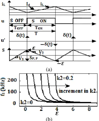
(b)
Figure 4. (a) Waveforms of the inductor current, switching pulse, time derivative of the control law and sliding surface in steady phase during the switching operation of the SMC; (b) Theoretical switching frequency of the designed SMC
TABLE 1. The parameters of the NOLC
Parameter Symbol Value
Input voltage E 12 V
Nominal output voltage VO 36 V
Inductor L 110 μH
Capacitor C1, C2 100 μF
Nominal load resistance R 50 Ω
Consider three state variables be 𝑧1= ∫ 𝑒, 𝑧2= 𝑒, 𝑧3= 𝑒′. Then, 𝑧1′= 𝑓
1(𝑧1, 𝑧2, 𝑧3) = 𝑧2, 𝑧2′= 𝑓2(𝑧1, 𝑧2, 𝑧3) = 𝑧3 and 𝑧3′= 𝑓3(𝑧1, 𝑧2, 𝑧3) = 𝑒′′. The third function can be determined from Equation (24) as follows:
𝑓3(𝑧1, 𝑧2, 𝑧3) = [𝑅(𝑎1𝐼𝑑− 𝑎3𝑧2−
𝑎4𝑧1)(𝑘1𝐸 + 𝑎3𝑧3+ 𝑎4𝑧2)2− 𝑎1(𝑅𝐶𝑧3+
𝑧2+ 𝑉𝑑)(𝑘1𝑧2+ 𝑘1𝑉𝑑+ 𝑘2𝑧3)(𝑘1𝐸 + 𝑎3𝑧3+
𝑎4𝑧2)− 𝑎2([𝑧3(𝑘1𝑧2+ 𝑘1𝑉𝑑+ 𝑘2𝑧3) +
(𝑅𝐶𝑧3+ 𝑧2+ 𝑣𝑑)𝑘1𝑧3][𝑘1𝐸 + 𝑎3𝑧3+ 𝑎4𝑧2] −
(𝑅𝐶𝑧3+ 𝑧2+ 𝑉𝑑)(𝑘1𝑧2+ 𝑘1𝑉𝑑+
𝑘2𝑧3)𝑎4𝑧3)]/(𝑎2[𝑅𝐶(𝑘1𝑧2+ 𝑘1𝑉𝑑+ 𝑘2𝑧3) +
(𝑅𝐶𝑧3+ 𝑧2+ 𝑉𝑑)𝑘2](𝑘1𝐸 + 𝑎3𝑧3+ 𝑎4𝑧2) −
𝑎3(𝑘1𝑧2+ 𝑘1𝑉𝑑+ 𝑘2𝑧3)(𝑅𝐶𝑧3+ 𝑧2+ 𝑉𝑑))
(25)
We define (p1,p2,p3) as the equilibrium point of the
obtained system. At this point, 𝑝1′= 𝑝2′= 𝑝3′= 0, with:
𝑓1(𝑧1, 𝑧2, 𝑧3) = 𝑓2(𝑧1, 𝑧2, 𝑧3) = 𝑓3(𝑧1, 𝑧2, 𝑧3) =
0 (26)
Solving (26), 𝑝2= 𝑝3= 0 and also:
𝑝1=𝑎𝑎1
4(𝐼𝑑−
𝑉𝑑2
𝑅𝐸) (27)
Therefore, there is an equilibrium point (𝑎1 𝑎4(𝐼𝑑− 𝑉𝑑2
𝑅𝐸) , 0,0) for the closed loop error system. If the origin
is a hyperbolic equilibrium point, the trajectories of a nonlinear system in a small region of neighborhood of an equilibrium point is close to the trajectories of its linearization in this region [18]. Proper selection of the PD-PI parameters ensures that the equilibrium point (𝑎1
𝑎4(𝐼𝑑− 𝑉𝑑2
𝑅𝐸) , 0,0) is hyperbolic. The Jacobian matrix
of the system around its equilibrium point is as follows:
𝐴1= [
𝑎11 𝑎12 𝑎13
𝑎21 𝑎22 𝑎23
𝑎31 𝑎32 𝑎33
] , 𝐵1= [
𝑏11 𝑏12
𝑏21 𝑏22
𝑏31 𝑏32
] (28)
where:
𝑎11= 𝑎13= 𝑎21= 𝑎22= 0, 𝑎12= 𝑎23= 1, 𝑎31=
𝑅𝑎4(𝑘1𝐸)2
𝑎3𝑘1𝑉𝑑2−𝑎2[𝑅𝐶𝑘1𝑉𝑑+𝑘2𝑉𝑑]𝑘1𝐸, 𝑎32=
−𝑅𝑎3𝑘12𝐸2+𝑎4𝑘1𝑎1𝑉𝑑2−2𝑎 1𝑘12𝐸𝑉𝑑
𝑎2[𝑅𝐶𝑘1𝑉𝑑+𝑘2𝑉𝑑]𝑘1𝐸−𝑎3𝑘1𝑉𝑑2 . 𝑎33=
2𝑅𝑘1𝑎3𝑎12𝐼𝑑2𝐸−𝑎1𝑅𝐶𝑘12𝐸𝑉𝑑−𝑎1𝑘1𝑘2𝐸𝑉𝑑−𝑎1𝑎3𝑘1𝑉𝑑2−2𝑎2𝑘12𝐸𝑉𝑑2+
𝑎2𝑎4𝑘1𝑉𝑑2
𝑎2[𝑅𝐶𝑘1𝑉𝑑+𝑘2𝑉𝑑]𝑘1𝐸−𝑎3𝑘1𝑉𝑑2
𝑏11= 𝑏12= 𝑏21= 𝑏22= 0, 𝑏31=
𝑅𝑎1(𝑘1𝐸)2
[𝑎2(𝑅𝐶𝑘1𝑉𝑑+𝑘2𝑉𝑑)𝑘1𝐸−𝑎3𝑘1𝑉𝑑2], 𝑏32=
−2𝑎1𝑘12𝐸𝑉𝑑
𝑎2(𝑅𝐶𝑘1𝑉𝑑+𝑘2𝑉𝑑)𝑘1𝐸−𝑎3𝑘1𝑉𝑑2−
𝑎2(𝑅𝐶𝑘1+𝑘2)𝑘1𝐸−2𝑎3𝑘1𝑉𝑑
(𝑎2(𝑅𝐶𝑘1𝑉𝑑+𝑘2𝑉𝑑)𝑘1𝐸−𝑎3𝑘1𝑉𝑑2)2
(29)
and also:
[ 𝑧̃̇1
𝑧̃̇2
𝑧̃̇3
] = 𝐴1[
𝑧̃1
𝑧̃2
𝑧̃3
] + 𝐵1[
𝐼̃𝑑
𝑉̃𝑑
where 𝑧̃1, 𝑧̃2, 𝑧̃3, 𝐼̃𝑑 and 𝑉̃𝑑 are the perturbations of 𝑧1, 𝑧2, 𝑧3, 𝐼𝑑 and 𝑉𝑑. Consider the desired eigenvalues of the proposed system to be λ1*, λ2* and λ3*. By using the pole
placement, it is given:
|
𝑠 − 𝑎11 −𝑎12 −𝑎13
−𝑎21 𝑠 − 𝑎22 −𝑎23
−𝑎31 −𝑎32 𝑠 − 𝑎33
| = (𝑠 − 𝜆1∗)(𝑠 −
𝜆2∗)(𝑠 − 𝜆3∗)
(31)
The system parameters are shown in Table 1. By using (31), the controller parameters can be determined as follows:
𝑎1= 1, 𝑘2= 0.2, 𝑎3= 0.72, 𝑎4= 140 (32) From Equation (25), it is concluded that the system has a discontinuous subspace. It is (𝑧1, −𝑉𝑑, 0) where z1 is any real point. Also, consider 𝐼𝑑=
𝑉𝑑2
𝑅𝐸. Figure 3 shows the phase portrait of the SMCC around (0,0,0). It is obviously understood that the equilibrium point is a stable node and it has a large attraction region. For all the initial points starting at [𝑧1(0), 𝑧2(0), 𝑧3(0)] with
𝑧2(0) > −𝑉𝑑, all the trajectories converge to origin.
Therefore, it is found that the error dynamics of the closed loop system around the origin is at least semi globally stable with a large attraction region, The aforementioned phase portrait is for S = 0. However, in practice, the voltage error will converge to a small layer around the desired output voltage. Therefore, the error variables oscillate around 0.
Due to the property of the integral term, interior term of the integrator should be zero. Therefore, the voltage error approaches to zero. Furthermore, by integrating the voltage error from zero time to settling time, the inductor current reference can be calculated. By reaching the sliding variable and voltage error to zero, the inductor current reaches to its generated reference. It is noticed that the internal dynamic (voltage of the middle capacitor) is limited between 0 V and input voltage. Therefore, this internal dynamic is always bounded.
2. 3. The Switching Frequency Analysis
According to the converter operation, it is supposed that three terms on the right side of Equation (10) are very small compared with other terms. Moreover, u is a step function. Thus, 𝑢′ is the Dirac delta function. When u steps up from 0 to 1, u’= 𝛿(𝑡) and when u steps down from 1 to 0, u′ = −𝛿(𝑡). The time derivative of S during the switch-OFF and switch-ON is:
{
𝑉1=
𝑑𝑆
𝑑𝑡|𝑢=1= 𝑘1𝐸 + 𝑘2𝛿(𝑡)𝑣𝑂− 𝑎3
𝑣𝑂
𝑅𝐶=
𝑆𝑃−𝑃
𝑇𝑜𝑛 > 0
𝑉2=
𝑑𝑆
𝑑𝑡|𝑢=0= 𝑘1𝐸 − 𝑘1𝑣𝑂− 𝑘2𝛿(𝑡)𝑣𝑂+ (
𝑎3
𝐶+ 𝑘2) 𝑖𝐿
−(𝑎3
𝐶+ 𝑘2)
𝑣𝑂
𝑅 =
−𝑆𝑃−𝑃
𝑇𝑜𝑓𝑓 < 0
(33)
where 𝑆𝑃−𝑃 is the hysteresis bandwidth of the controller comparator. Also, 𝑇𝑜𝑛 and 𝑇𝑜𝑓𝑓 are the ON and OFF time
intervals in a time period of the switching operation, respectively. V1 and V2 are the speed of the designed
sliding variable in the two states. The switching operation of the SMC and waveforms of 𝑖𝐿, 𝑢, u′ and S are shown in Figure 4a. S oscillates between – 𝜀 and 𝜀 by a hysteresis controller with speed of V1 in ON state and
speed of V2 in OFF state around zero; i.e.,
𝑆𝑃−𝑃= 2𝛆 (34)
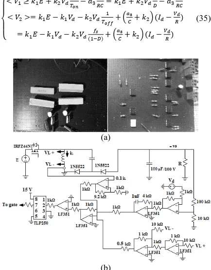
From Equation (33), it is concluded that the speed of S is dependent on the Dirac delta function in both ON and OFF modes. From both theoretical and practical point of view, it is understood that the sliding surface is moved between – 𝜀 and 𝜀 with infinite speed. Therefore, the high frequency operation can be achieved. By using Equation (33), the average value of V1 and V2 are given as follows:
{
< 𝑉1≥ 𝑘1𝐸 + 𝑘2𝑉𝑑
1
𝑇𝑜𝑛− 𝑎3
𝑉𝑑
𝑅𝐶= 𝑘1𝐸 + 𝑘2𝑉𝑑
𝑓𝑠
𝐷− 𝑎3
𝑉𝑑
𝑅𝐶
< 𝑉2>= 𝑘1𝐸 − 𝑘1𝑉𝑑− 𝑘2𝑉𝑑
1
𝑇𝑜𝑓𝑓+ (
𝑎3
𝐶 + 𝑘2) (𝐼𝑑−
𝑉𝑑
𝑅)
= 𝑘1𝐸 − 𝑘1𝑉𝑑− 𝑘2𝑉𝑑
𝑓𝑠
(1−𝐷)+ (
𝑎3
𝐶+ 𝑘2) (𝐼𝑑−
𝑉𝑑
𝑅)
(35)
(a)
(b)
Figure 5. The structure of the developed system; (a) the set-up of the system; (b) schematic diagram of the controller
(a) (b)
Figure 6. The practical switching frequency with the proposed PD-PI SMC and conventional strategy for VO=36V and different input voltages; (a) R=100Ω; (b)
where fS is the switching frequency and D is the duty
cycle of the converter, i.e.:
𝐷 = 𝑇𝑜𝑛
𝑇𝑜𝑛+𝑇𝑜𝑓𝑓=
𝑉𝑑−𝐸
𝑉𝑑 (36)
By using Equations (34)-(36), the switching frequency of the proposed SMC can be obtained as follows:
𝑓𝑠=𝑇 1
𝑜𝑛+𝑇𝑜𝑓𝑓=
1
2𝜀 <𝑉1> −
2𝜀 <𝑉2>
=
1
2𝜀
𝑘1𝐸 +𝑘2𝑉𝑑
2
𝑣𝑑−𝐸𝑓𝑠−𝑎3𝑉𝑑𝑅𝐶
− 2𝜀
𝑘1𝐸 − 𝑘1𝑉𝑑− 𝑘2𝑉𝑑
2
𝐸 𝑓𝑠+(𝑎3𝐶 +𝑘2)(𝐼𝑑−𝑉𝑑𝑅 )
(37)
Here, the switching frequency must be numerically obtained. We define 𝜀𝐶 as a critical hysteresis bandwidth in CCM. If 𝜀 < 𝜺𝑪, the switching frequency converges to infinite. If the frequency largely increases, then 𝑘2𝑣𝑑2
𝑣𝑑−𝐸𝑓𝑠≫ (𝑘1𝐸 − 𝑎3
𝑉𝑑
𝑅𝐶) and
𝑘2𝑣𝑑2
𝐸 𝑓𝑠≫ (𝑘1𝑉𝑑− 𝑘1𝐸 +
(𝑎3
𝐶 + 𝑘2) (𝐼𝑑− 𝑉𝑑
𝑅)). By using Equation (37) and these
assumptions, 𝜀𝐶 can be determined as follows:
𝜀𝐶=𝑘22𝑉𝑑 (38)
The switching frequency is shown in Figure 4. It is obvious that the coefficient k2 largely impacts on the
frequency. If this parameter increases, then 𝜀𝐶 will effectively increase. Therefore, high switching frequency is achieved when there exists a large time delay or hysteresis bandwidth in practice. To construct derivative of the current for the defined sliding variable as shown in Figure 1, this paper uses the following relationship:
𝑎1 𝑑𝑖𝐿
𝑑𝑡 = 𝑘2𝑣𝐿 (39)
4. PRACTICAL RESULTS
An experimental set-up of the developed system was constructed. Figure 5a shows the photograph of the NOLC with the designed PD-PI based SMC. IRFZ44N and MBR20150C are selected as power switch and diodes. Also, three parallel inductors with ferrite cores and the value of 110 μH/9A and two electrolytic capacitors with the value of 100 μF/100 V are used for power converter. The current is measured using the ACS712-20A sensor and voltage measurement is done applying the resistive dividers. The photograph of the NOLC with the controller is shown in Figure 5b. In this work, the low slew rate OP-AMP LF351 is used for the signal amplification and hysteresis modulation to show the efficacy of the proposed controller for the switching frequency enhancement. In order to show the system robustness, the desired inductor current is disabled. Furthermore, the Rigol oscilloscope is used to save the practical tests and WFM Viewer software is used to show the obtained results in computer.
Figures 6a, b show the measured switching frequency with the proposed approach and conventional SMC operated in CCM against line variations for R=100, 50 Ω, respectively. From these figures, it is observed that the practical frequency increases from the interval (7 14) to (170 200) kHz. Also, the ratio of the switching frequency variations to the average value of the switching frequency of the PD-PI based SMC is less than conventional SMC for the aforementioned points.
Consider Vo=36V, R=100 Ω. Figures 7a and b show the steady waveforms of the current and generated control pulse of the NOLC in CCM for E=24 and E=18 V, respectively. It is clear that the converter under the proposed SMCC can works in CCM at low voltage gains and light loads. Furthermore, the sliding variable of the developed SMCC for E=18V, VO=36 V and R=100 Ω is
depicted in Figure 7c. This figure shows that the hysteresis bandwidth is about 8V. This value is so large, because of the large time delays of the circuit components. Hence, the experimental frequency of the conventional SMC effectively decreases. Moreover, the bandwidth is asymmetrical in practice.
Consider 𝑉𝑑= 36 𝑉, 𝐸 = 12 𝑉 and 𝑅 = 50 Ω. The system starts from the initial points of 𝑉𝑂(0) = 0 𝑉 and
𝑖𝐿(0) = 0 𝐴.
(a)
(b)
(c)
Figure 7. The steady performance of the system at low voltage gains; (a) inductor current and gate pulse waveformrs for E=24 V, R=100 Ω and VO=36; (b) nductor
current and gate pulse waveformrs for E=18 V, R=100 Ω and VO=36; (c) the sliding variable for E=18V, VO=36 V and
The practical result for this condition is shown in Figure 8a. In addition, Figure 8b illustrates the system response using the PD_PI type SMCC for 𝑉𝑑= 36 𝑉, 𝐸 =
15 𝑉 and 𝑅 = 50 Ω.
Consider VO=36V. The load resistance steps-down
from 200 to 50Ω and vice versa. Figures 9a and b depicts the system responses agaisnt load variation for E=12 and 18, respectively. In these figures, the voltage well follows its reference after the load change. Figure 10a shows the system response during transient region for R=100Ω, E=12V and the voltage variation from about 35 to 49V. This figure demonstrates that the output variable has a good behavior. Also, the overshoot is 1V with settling time of about 20ms. Figure 10b shows the practical response for R=100Ω, E=12V and the voltage change from about 36 to about 22V. For this test, the voltage overshoot equals to about 6V and settling time of about 30ms. Figure 11c depicts the voltage behavior for E=12V, R=36Ω and voltage reference variation from nearly 36 to about 22V. For this experiment, the settling time is about 40ms.
(a) (b)
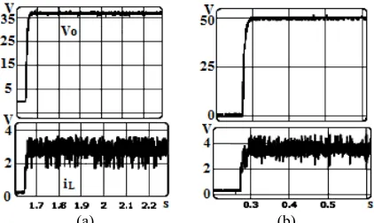
Figure 8. The transient response for R=50 Ω; Ω (a) VO=36
V, E=12 V; (b) VO=50 V, E=18 V
(a) (b)
Figure 9. The practical results for load variation from 200 to 50 (a) E=12 V, 𝑉𝑂= 36 𝑉; (b) E=18 V, 𝑉𝑂= 36 𝑉
5. CONCLUSIONS
This study proposes a PD-PI type sliding mode current controller for a NOLC in CCM operation. A systematic
guideline for designing, developing and analyzing the characteristics of a cascade controller has been provided in the paper which includes proper choice of the sliding variable, investigation of the stability conditions and determination of the theoretical equation for the switching frequency. It is established that utilization of a PD compensator effectively enhances the switching frequency as compared with conventional sliding mode controller. By means of the suggested sliding variable, the minimum and maximum switching frequency increase from 7 and 14kHz to 150 and 200kHz for the aforementioned conditions, respectively. Furthermore, it is experimentally verified that the designed control scheme can well adjust the converter voltage with no steady error in presence of important disturbances in the uncertain parameters. It is said that the abrupt changes do not happen in practical applications at a same time. However, the practical experiments show high-accuracy trajectory tracking of the overall system for a strong system robustness and fast response against these abrupt variations.
6. REFERENCES
1. Prabhakar, M., “High gain dc-dc converter using active clamp circuit (research note)”, International Journal of
Engineering-Transactions A: Basics, Vol. 27, No. 1, (2013), 123-130.
2. Adell, P. C., Witulski, A. F., Schrimpf, R. D., Baronti, F., et al., “Digital control for radiation-Hardened switching converters in space”, IEEE Transactions on Aerospace and Electronic
Systems, Vol. 46, No. 2, (2010), 761-770.
3. Goudarzian, A., Nasiri, H., Abjadi, N., “Design and implementation of a constant frequency sliding mode controller for a Luo converter”, International Journal of
Engineering-Transactions B: Applications, Vol. 29, No. 2, (2016), 202-210.
4. Forouzesh, M., Siwakoti, Y., Gorji, A., Blaabjerg, F., Lehman, B., “Step-up dc/dc converters: a comprehensive review of voltage boosting techniques, topologies, and applications”, IEEE
Transactions on Power Electronics, Vol. 32, No. 12, (2017),
9143-9178.
5. Babu, R., Deepa, S., Jothivel, S., “A closed loop control of quadratic boost converter using PID-controller”, International
Journal of Engineering-Transactions B: Applications, Vol. 27,
No. 11, (2014), 1653-1662
6. Sarvi, M., Derakhshan, M., Sedighi Zade, M., “A new intelligent controller for parallel dc/dc converters”, International Journal of
Engineering-Transactions B: Basics, Vol. 27, No. 1, (2014),
131-142
7. Suntio, T., “On dynamic modeling of PCM-controlled converters-buck converter as an example”, IEEE Transactions on Power
Electronics, Vol. 33, No. 6, (2017), 5502-5518.
8. Abjadi, N. R., Goudarzian, A. R., Arab Markadeh, Gh. R., Valipour, Z., “Reduced-order backstepping controller for POESLL DC/DC converter based on pulse width modulation”, Iranian Journal of Science and Technology, Transactions of
Electrical Engineering, (2018), To be
published:doi.org/10.1007/s40998-018-0096-y(01
of Engineering-Transactions C: Aspects, Vol. 30, No. 12 (2017) 1879-1884
10. Vali, M. H., Rezaie, B., Rahmani, Z., “Designing a neuro-sliding mode controller for networked control systems with packet dropout”, International Journal of Engineering-Transactions
A: Basics, Vol. 29, No. 4, (2016), 490-499.
11. Goudarzian, A., Khosravi, A., “Design, analysis, and implementation of an integral terminal reduced‐order sliding mode controller for a self‐lift positive output Luo converter via Filippov's technique considering the effects of parametric resistances”, International Transactions on Electrical and
Energy Systems, (2018), e2776.
https://doi.org/10.1002/etep.2776.
12. Nasiri, H., Goudarzian, A., Pourbagher, R., Derakhshandeh, S. Y., “PI and PWM sliding mode control of POESLL converter”,
IEEE Transactions on Aerospace and Electronic Systems, Vol.
53, No. 5, (2017), 2167-2177.
13. Qi, W., Li, S., Tan, S. C., Hui, S., “Parabolic-modulated sliding mode voltage control of buck converter”, IEEE Transactions on
Industrial Electronics, Vol. 65, No. 1, (2018), 844-854.
14. Zhao, Y., Qiao, W., Ha, D., “A sliding mode duty ratio controller for dc/dc buck converters with constant power loads”, IEEE
Transactions on Industrial Applications, Vol. 50, No. 2, (2014),
1448-1458.
15. Mamarelis, E., Petrone, G., Spagnuolo, G., “Design of a sliding-mode-controlled SEPIC for PV MPPT applications”, IEEE
Transactions on Industrial Electronics, Vol. 61, No. 7, (2014),
3387-3398.
16. Vidal-Idiarte, E., Carrejo, C. E., Calvente, J., Martínez-Salamero, L., “Two-loop digital sliding mode control of dc/dc power converters based on predictive interpolation”, IEEE
Transactions on Industrial Electronics, Vol. 58, No. 6, (2011),
2491-2501.
17. Bhat, S., Nagaraja, H. N., “DSP based proportional integral sliding mode controller for photo-voltaic system”, International
Journal of Electrical Power & Energy Systems, Vol. 71, (2015),
123-130.
18. Knalil, H. K. Nonlinear Systems. Upper Saddle River, NJ: Prentice-Hall, (2002).
Voltage Regulation of a Negative Output Luo Converter Using a PD-PI Type Sliding
Mode Current Controller
A. Goudarzian, A. Khosravi
Department of Electrical Engineering, Faculty of Engineering, Shahrekord Branch, Islamic Azad University, Shahrekord, Iran
P A P E R I N F O
Paper history:
Received 19 September 2018
Received in revised form 19 November 2017 Accepted 03 Januray 2019
Keywords:
Switching Converter
Negative Output Luo Converter PD-PI Type Sliding Surface Control Design
هدیکچ
عون دیدج یشزغل دم هدننک لرتنک کی هلاقم نیا
PD-PI
لدبم یارب
NOLC
یم هئارا هتسویپ تیاده تلاح رد .دهد
رطاخب
ژاتلو و یدورو نایرج میظنت و لدبم درکلمع دوبهب یارب .تسا یطخریغ تدش هب لدبم کیمانید ،یورو ژاتلو و راب تارییغت لرتنک .تسا زاین یطخریغرلتنک کی ،لدبم یجورخ ناشن یلمع جیاتن .تسا لدبم هدیچیپ تاذ اب بسانتم یداهنشیپ هدننک
دنتسه یداهنشیرلرتنک بوخ رایس درکلمع هدنهد کبس رایسب یاهراب رد ار لدبم ،ژاتلو مئاد یاطخ فذح اب تسا رداق هک
.دنک لرتنک فلتخم یراک طاقن رد لااب ینزدیلک سناکرف و
doi: 10.5829/ije.2019.32.02b.13