Printed in The Islamic Republic of Iran, 2010 © Shiraz University
CONSTANT INPUT POWER CONTROL OF THREE-PHASE
ISOLATED BUCK+BOOST RECTIFIER
*A. MOHAMMADPOUR AND M. R. ZOLGHADRI
**Dept. of Electrical Engineering, Sharif University of Technology, Tehran, I. R. of Iran Email: [email protected]
Abstract– A novel control method is proposed for single-stage three-phase isolated buck+boost rectifier. The control method is based on the conventional cascade two-loop control structure and is modified to achieve constant instantaneous input power. Input voltages, output voltage, and DC-link inductor current are measured to control the power switches to achieve output voltage regulation as well as input power factor correction. In the proposed method, input currents are controlled such that input power is constant, even for unbalanced mains. Thus, for the balanced mains converter it behaves like an ideal rectifier, and for unbalanced mains, low-frequency harmonics of the output voltage are suppressed. The performance of the proposed control structure is verified by the numerical simulation of a 6kW, 380V/48Vdc designed prototype.
Keywords– Three-phase single-stage power supply, buck+boost rectifier, unbalanced mains, power factor correction
1. INTRODUCTION
A typical telecom power supply should provide regulated dc voltage to the load with the following features:
• Low (Total Harmonic Distortion) THD of input currents to meet international standard requirements such as IEC 61000-3-2
• Unity input power factor • Input-output electrical isolation
• High efficiency (more than 90% at full load) • High power density
• Acceptable output for unbalanced mains • Low cost
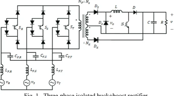
These requirements motivate the design of three-phase single-stage (Power factor Correction) PFC rectifiers compared to conventional two-stage structures. A boost-type AC-DC converter is presented in [1] for both single-phase and three-phase structures. Unity power factor three-switch isolated buck rectifier is proposed in [2] for three-phase AC-DC conversion. This structure is derived from three-phase three-switch buck rectifier [3], where high frequency isolation is achieved by introducing a forward converter. A three-phase single-stage isolated buck+boost rectifier for telecommunication power supply modules is proposed in [4]. The schematic of the proposed circuit and system specifications are shown in Fig. 1 and Table 1. This structure is topologically equivalent to the converter described in [2], and is controlled with the control method of [5], [6] to have a unity power factor, even for unbalanced input voltages. The problem with this control concept is the output voltage low-frequency harmonics for the
unbalanced mains condition. In literature some works are carried out for harmonic elimination in boost-based rectifiers [7-9]. One method for output voltage harmonic suppression is presented in [10] for a six switch buck rectifier which eliminates a limited number of harmonic frequencies.
Fig. 1. Three-phase isolated buck+boost rectifier
Table 1. Operating point for design and simulation
Parameter Value
Input filter inductor Lf 240μH
Input filter capacitor Cf 6.8μF
Output capacitor Co 40mF
Output inductor Lo 200μH : :
p s d
N N N 10:3:1
Magnetizing inductanceLm 4mH
In this paper a new control structure is proposed to eliminate the aforementioned low-frequency harmonics in the case of the unbalanced mains without the performance degradation for the balanced mains condition. The proposed control method utilizes the DC-link current sensor instead of AC current sensors. This control technique is advantageous to the load since the output filter capacitance can be minimized with a minimal output DC voltage ripple.
In section 2, the operation of a converter with resistive input control method is reviewed. The principle of constant input power control is discussed briefly in section 3. The proposed control structure for constant input power is presented in section 4. The numerical simulation results are provided in section 5 to verify the validity of the theoretical concepts. Section 6 summarizes the results of the proposed control method.
2. THREE-PHASE ISOLATED BUCK+BOOST RECTIFIER WITH RESISTIVE INPUT CURRENT METHOD
An optimized space vector modulation method was developed in [11] for non-isolated buck converter considering switching loss, ripple values, and mains current quality. The modulation method of [11] is not directly applicable to the isolated buck rectifier and is modified in [4] to prevent transformer core saturation. One mains period is divided into 12 sectors based on the input phase voltages relation. The switching state sequence for the first sector of the mains is shown in Fig. 2, where j=(s s sR S T)indicates a combination of the three input buck switches, si=1 shows on-state, and si=0 off state of the according switch. The switching states with only one conducting bridge leg cannot be applied in the freewheeling state, and (000) is applied in this case to ensure complete demagnetization of the transformer. For balanced mains, the buck stage modulation index M isdefined as
2
,
(0;1)
3
p o
s VN
N V
M
M
N
=
∈
(1)where VN is the peak value of the phase-to-neutral voltage and Vo is the dc-link voltage. Maximum modulation index, Mmax, is limited such that the transformer is completely demagnetized during the freewheeling state max ,min ,max
1
1.5
1
d Np o
M
V
N
N
V
=
+
(2)The output boost stage has to be activated only for a combination of input and output voltages which results in M >Mmaxin this case
N p
s M V
N N
V0 max
2 3
= (3)
This is smaller than the desired output voltage. Therefore, the duty cycle of the boost switch is determined by o ref ref
V
V
V
δ
=
−
(4)Fig. 2. Switching state sequence for the first mains sector
For unbalanced mains the maximum average value of buck stage output voltage within a switching cycle is defined as
$
,max
3
max2
s
o N
p
N
v
M
v
N
=
(5)$
, , ,
2 2 2
2( )
3 F R F S F T
N C C C
For Vo<vo,max, v$N >VN,min the buck input stage operates at a modulation index smaller than the maximum modulation index, and the boost output stage duty cycle is zero. For M >Mmaxthe boost stage has to be activated with ,max o ref ref v v v
δ
= − (7)Calculation of the relative on-times of the power transistors for the resistive input power method is discussed in [4]. For example, the relative on-times for the first mains sector are given in Eqs. (3) and (4),
,
, , ,
,
101 2 2 2 F T
F R F S F T
p o ref
C
s C C C
v
N
v
N v
v
v
δ
=
+
+
(8),
, , ,
,
110 2 2 2 F S
F R F S F T
p o ref
C
s C C C
v
N
v
N v
v
v
δ
=
+
+
(9)The relative on-time of the freewheeling state is evaluated based on the fact that the sum of the relative on-times during a switching period has to be equal to one.
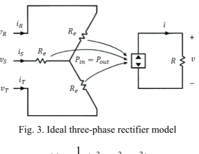
With the resistive input currents method, the converter is similar to the ideal three-phase rectifier as depicted in Fig. 3. Total instantaneous input power is
Fig. 3. Ideal three-phase rectifier model
2 2 2
1
( ) ( )
in R S T
e
p t v v v
R
= + + (10)
For balanced mains, the second harmonic of the input power is added to zero and the rectifier can supply constant instantaneous input power to a DC load. For unbalanced mains the input power has a second harmonic term which results in output voltage ripple.
3. CONSTANT INPUT POWER METHOD PRINCIPLES
( v) ( v)
j t j t
in
Vuur =Vuuur uuur++V− =V e+ ω θ+ + +V e− − +ω θ− (11)
( i ) ( i )
j t j t
in
I =uur uurI++I−=I e+ ω θ+ + +I e− − +ω θ−
ur
(12)
where ,V V I Iuur uur uur uur+ −, ,+ − are input positive and negative sequence voltage and current vectors. V V I I+, −, ,+ − are the magnitude of the positive and negative sequence voltage and current vectors. θ θ θ θv+, v−, i+, i− are
the phase angle of the positive and negative sequence voltage and current vectors. Thus the input apparent power is
* ( ) ( ) (2 ) ( 2 )
v i v i v i v i
j j j t j t
in
in in in in
S
=
P
+
jQ
=
V I
=
V I e
+ + θ θ+− ++
V I e
− − θ θ−− −+
V I e
+ − ω θ θ+ +− −+
V I e
− + −ω θ θ+ −− +ur uur ur
(13)
In order to make input power constant and eliminate the low-frequency ripples of the output voltage, Eqs. (14) and (15) must be satisfied [8], [9]:
V
I
V
I
+ +
−
=
− (14)v i i v
θ
+ −θ
+ =θ
−−θ
−−π
(15)An additional condition is imposed to have a unity power factor for balanced mains [8],
v i
θ
+ =θ
+ (16)If Eqs. (13), (14) and (15) are satisfied, the active and reactive input powers are
in
P =V I+ + −V I− − (17)
( )sin(2 )
in v i
Q = V I+ −+V I− +
ω θ
t+ +−θ
− (18)It can be seen that the instantaneous input power is constant and low-frequency harmonics are eliminated for unbalanced mains. Furthermore, for balanced mains, constant input power is equivalent to the unity power factor operation [7].
4. CONSTANT INPUT POWER CONTROL METHOD FOR THREE-PHASE ISOLATED BUCK+BOOST RECTIFIER
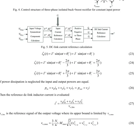
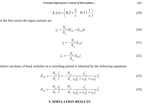
The proposed control structure is depicted in Fig. 4. This control structure is similar to the resistive input control structure [4], [5]. The main difference is in the link current reference calculation. In [5] a dc-current shaping block was used to control the dc-link inductor dc-current to achieve the sinusoidal mains currents in-phase with the input voltages for unbalanced mains. For the constant input power method, the dc-current shaping block is replaced with the harmonic elimination block. Details of the harmonic elimination block for reference dc-link current evaluation in constant input power method is depicted in Fig. 5. Output voltage controller is a single-input multi-output system with two outputs. These outputs are used to regulate the magnitude and phase of input current sequence components. The magnitudes of the positive and negative sequence components of the input currents are given by
*
,1 ( )
C ref
I+=i V V+ −V (19)
*
,1 ( )
C ref
I− =i V V− −V (20)
where * ,1 C
*
,2( )
i v iC Vref V
θ
+ =θ
+− − (21)
*
,2( )
i v iC Vref V
θ
−=θ
−+ +π
− (22)where * ,2 C
i is the second output of the voltage controller. Using the reference values of magnitude and the phase of positive and negative sequence input currents, the reference values of three phase input currents are calculated.
Fig. 4. Control structure of three-phase isolated buck+boost rectifier for constant input power
Fig. 5. DC-link current reference calculation
*
( )
sin(
)
sin(
)
i i
R
i t
=
I
+ω θ
t
+
++
I
−ω θ
t
+
− (23)*( ) sin( 2 ) sin( 2 )
3 3
i i
S
i t =I+
ω θ
t+ +−π
+I−ω θ
t+ −+π
(24)*( ) sin( 2 ) sin( 2 )
3 3
i i
T
i t =I+
ω θ
t+ ++π
+I−ω θ
t+ −−π
(25)If power dissipation is neglected the input and output powers are equal.
in R R S S T T out o
p =v i +v i +v i = p =v i (26)
Then the reference dc-link inductor current is evaluated
* * *
*
,lim
R R S S T T
o
v i v i v i
i
v
+ +
= (27)
,lim o
v is the reference signal of the output voltage where its upper bound is limited by vo,max
, , ,
2 2 2
,max max
3
2
(
)
2
3
F R F S F T so C C C
p
N
v
M
v
v
v
N
=
+
+
(28)2
1
( )
0.2
0.1
v
k s
s
s
⎛
⎞
⎜
⎟
⎝
⎠
=
+
+
(29)For the first sector the input currents are
101 110 ( ) s R p N i i
N
δ
δ
= + (30)
110 s S p
N
i
i
N
δ
= −
(31)101 s T p N i i N
δ
= − (32)
Relative on-times of buck switches in a switching period is obtained by the following equations
* *
*
110 * * * *
p s p o
S
s s R R S S T T
N
i
N
v
i
N i
N v i
v i
v i
δ
= −
= −
+
+
(33)* *
*
101 * * * *
p T p o
T
s s R R S S T T
N
i
N
v
i
N i
N v i
v i
v i
δ
= −
= −
+
+
(34)5. SIMULATION RESULTS
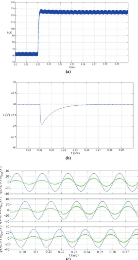
In this section the simulation results of a converter are presented to verify the validity of the proposed control method. For balanced mains condition the converter behavior is similar to an ideal three phase rectifier. DC-link inductor current and the output voltage of the converter for load change from a half-load to a full-load condition are displayed in Figs. 6a and 6b. It can be seen that the current loop shows a fast dynamic response, but the voltage loop is slower. However, the voltage decrease for this load change is smaller than 1 V and response time is 0.04 seconds. From Fig. 6c the input currents are in-phase and proportional to the input voltage in both cases.
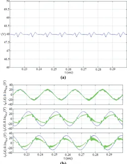
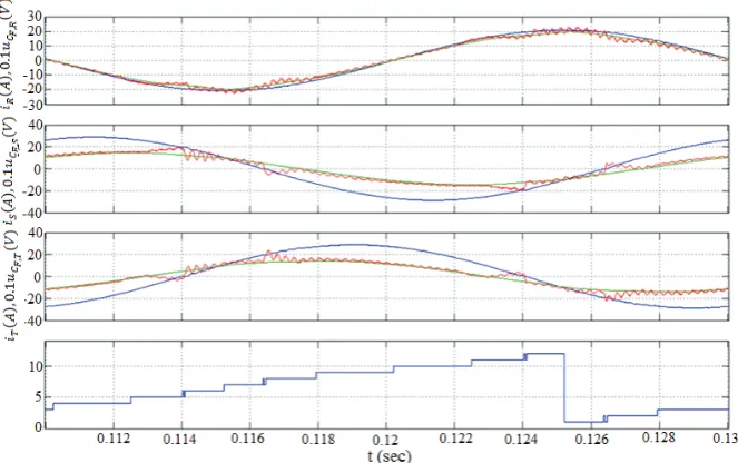
In order to investigate the performance of the control structure for the unbalanced mains condition, the simulation results are presented for 5% and 50% voltage reduction in one phase voltage. If the power loss of the converter is neglected, the input power is proportional to the square of the output voltage for a resistive load. So the output voltage ripple is used as an indicator of output and input power oscillations. The output voltage of the converter for 5% decrease in the voltage of phase R (equivalent to 1.7% voltage unbalance factor according to IEC definition [12]) is shown in Fig. 7a. The peak-to-peak ripple value is 0.02V and average THD of the input currents is 4.5%. Input currents are sinusoidal and in-phase with corresponding input voltages as depicted in Fig. 7b. The performance of the system for heavily unbalanced mains condition is analyzed with 50% voltage reduction in phase R voltage (equivalent to 17% voltage unbalance factor according to IEC definition). The simulation results for this case are displayed in Fig. 8. The peak-to-peak output voltage ripple is 0.2V and the average THD of the input the currents is 15%. Since the input currents must have the same polarity as the corresponding input voltages, they do not track the input voltages in the proximity of their zero crossings (Fig. 9). This results in waveform distortion in the input and output of the converter.
in one phase voltage also shows that output voltage ripple is considerably lower for constant input power method. For unbalanced mains condition, input current THD is high for constant input power method compared to resistive input method. This is not important because the unbalanced condition is temporary. It is noteworthy that the proposed method cannot eliminate low-frequency ripple of the output voltage for two-phase operation (loss of one phase). In this case instantaneous input power is pulsating, which will result in the output voltage second harmonic ripple.
(a)
(b)
(c)
(a)
(b)
Fig. 7. Simulation result for 5% decrease in the voltage of phase R, (a) output voltage, (b) input voltage and current
(a)
(b)
Fig. 9. Input voltages, input currents, input currents references and sector number for an input line period for 50% decrease in the voltage of phase
Table 2. Comparison of output voltage ripple value in the proposed control method with 2 other methods
Resistive Input characteristic Constant input power
Voltage decrease in Phase R (%)
0.28 0.01
5
1.7 0.05
25
3.8 0.2
50
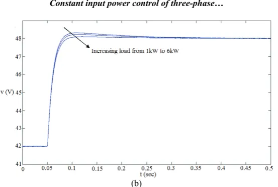
Based on the equations for small-signal modeling of the system, the dynamic behavior of the system depends on the power stage component values, input and output voltages, and load value [5]. Finally, in order to verify the robustness of the control system against these uncertainties, the dynamic response for different operating points is investigated by simulation. Fig 10a shows the output voltage for load change from half-load to full-load for three values of the input voltage. It can be seen that the dynamic response of the output voltage does not depend on the input voltage value except for a small difference in the output voltage decrease. Output voltage of the converter, when reference voltage changes from 42 V to 48 V is shown in Fig. 10(b) for three load values (1kW, 3kW, 6kW). The results of simulation demonstrate the negligible effect of these uncertainties on system stability and transient response.
(a)
(b)
Fig. 10. Robustness of control system against (a), input voltage variations, (b) load variations
6. CONCLUSION
A new control structure is proposed for three-phase isolated buck+boost rectifier. This control method offers good dynamic response and shows a resistive characteristic in the input for balanced input voltages. In this case the input currents are in-phase and proportional to the corresponding input voltages. Furthermore, with this control strategy low-frequency harmonics from the input and output of the converter are eliminated for unbalanced mains. Only DC-link inductor current is measured instead of AC input currents. It is apparent that due to the single-stage structure of the converter, constant input power method is not realizable for two-phase operation.
REFERENCES
1. Khoei, A. & Yuvarajan, S. (2000). Application of rectified-voltage PWM for power factor correction. Iranian Journal of Science and Technology, Transaction B: Enginnering, Vol. 24, No. B1.
2. Greff, D. & Barbi, I. (2006). A single-stage high-frequency isolated three-phase AC/DC converter. IEEE IECON’06, The 32nd Annual Conference of the IEEE Industrial Electronics Society.
3. Malesani, L. & Tenti, P. (1987). Three-phase AC/DC converter with sinusoidal ac currents and minimum filter requirements. IEEE Trans. Ind. Appl., Vol. IA-23, No.1, pp. 71-77.
4. Mohammadpour, A. & Zolghadri, M. R. (2009). Control of three-phase single-stage isolated buck+boost unity power factor rectifier for unbalanced input voltages. Proceedings of the 4th IEEE International Conference on
Electric Power and Energy Conversion Systems (EPECS), Sharjah, UAE.
5. Nussbaumer, T., Guanghai, G., Heldwein, M. L. & Kolar, J. W. (2008). Modeling and robust control of a three-phase Buck+Boost PWM rectifier (VRX-4). IEEE Trans. Ind. Appl., Vol. 44, No. 2, pp. 650 – 662.
6. Baumann, M. & Kolar, J. W. (2007). A novel control concept for reliable operation of a phase three-switch buck-type unity-power-factor rectifier with integrated boost output stage under heavily unbalanced mains condition. IEEE Trans. Ind. Electron., Vol. 52, No. 2, pp. 399–409.
7. Jin, A., Li, H. & Li, S. (2006). A flexible input currents control strategy for three-phase PFC rectifier under unbalanced system. Proc. 1st IEEE Industrial Electronics and Applications, pp. 1-6.
8. Stankovic, A.V. & Lipo, T. A. (2001). A novel control method for input output harmonic elimination of the PWM boost type rectifier under unbalanced operating conditions. IEEE Trans. Power Electron, Vol. 16, No. 5, pp. 603 – 611.
10. Enjeti, P. N. & Choudhury, S. A. (1993). New control strategy to improve the performance of a PWM AC to DC converter under unbalanced operating conditions. IEEE Trans. Power Electron, Vol. 8, No. 4, pp. 493–500. 11. Nussbaumer, T., Baumann, M. & Kolar, J. W. (2007). Comprehensive design of a three-phase three-switch
buck-type PWM rectifier. IEEE Trans. Power Electron, Vol. 22, No. 2, pp. 551-562.