International Journal of Engineering
J o u r n a l H o m e p a g e : w w w . i j e . i r
T. Sarkar*, S. Nath Pradhan
Department of ECE, National Institute of Technology, Agartala. Agartala, India
P A P E R I N F O
Paper history: Received 17 March 2017
Received in revised form 13 January 2018 Accepted 08 March 2018
Keywords: Testing Don’t Care Run Time Leakage Fault Coverage Genetic Algorithm Test Pattern Ordering Pattern Dependency
A B S T R A C T
Estimating and minimizing the maximum power dissipation during testing is an important task in VLSI circuit realization since the power value affects the reliability of the circuits. Therefore during testing suitable methodologies should be adopted to minimize power consumption. Test patterns generated with –D 1 option of ATALANTA contains don’t care X bits. By suitable filling of don’t cares can minimize the number of switching activity between two successive patterns. The switching power dissipation of the Circuit under Test (CUT) also depends on the order of patterns applied for testing. If consecutive pattern application time is sufficiently large then leakage power dissipation does not alter on the ordering of the patterns. So under this circumstances leakage power does not change but if the pattern application time is small leakage power depends on the ordering of the pattern applied to the CUT. Previous works concern only about don’t care filling or pattern ordering or first filling of don’t care and then ordering for low power circuit testing. Ordering after filling of don’t care may change the benefits of X-filling. The advantage of test power reduction of both the methods - don’t care filling and ordering may be obtained if they are considered together. In this work an approach based on Genetic Algorithm (GA) is used to solve the integrated problem for X-filling and reordering of test patterns considering pattern dependency to minimize the switching activity throughout testing without changing the fault coverage. Effectiveness of the proposed GA based approach compared to existing approach considering test patterns for ISCAS’85 benchmark circuits is shown in the result section.
doi: 10.5829/ije.2018.31.05b.10
1. INTRODUCTION1
Reduction of power consumption at the time of circuit testing becomes a challenging issue as the design consumes more power in test mode compared to functional mode of operation [1]. At present, testing is one of the most vital issues in the development process of an integrated circuit. The issues that depends on testing are manufacturing yield, test cost and product quality [2-4].
It was shown that test power is much higher than the power consumption in normal functional mode due to several reasons such as (i) Automatic test pattern generation (ATPG) tools generate test patterns that have high toggle rate in order to reduce pattern count and test application time. Therefore the switching activity of the circuit in test mode is often several times higher compared to normal mode of operation. (ii) To reduce
*Corresponding Author Email: [email protected](T. Sarkar)
test application time parallel testing is also used, mainly for System-on-Chip (SOC) devices. This parallelism increases power dissipation during test. (iii) The Design-for-Testability (DFT) circuitry is inserted in the circuit under test to improve testing issues. DFT circuit remains idle at normal operation but is used in test mode. These additional active elements further increase power dissipation. In this work single stuck-at fault model is considered. In this fault model the value on the faulty signal line appears to be stuck either at logic ‘0’ or logic ‘1’, referred to as stuck-at-0 or stuck-at-1 respectively. Test patterns are generated using ATALANTA tool. CAD tool- ATALANTA generates test patterns targeting stuck-at fault.
Most of the works related to power reduction in the literature describes about dynamic power minimization. But as the technology shrinks down below 65nm leakage power dominates over dynamic power. So, minimizing
Test Power Reduction by Simultaneous Do
n
o
t Care Filling and Ordering of
Test Patterns Considering Pattern Dependency
leakage power has become an important task in overall power minimization of the circuit. It is considered that leakage power depends only on the current input pattern applied to the circuit. But runtime leakage power [5] depends on both the previous and present input pattern applied to circuit [6] and this runtime leakage power also changes with the change of test application time. So, leakage power depends not only on the order of test patterns applied to the circuit but also on the applied time period. Also dynamic power depends on the switching activity between test patterns fed to the test circuit. So, dynamic power depends on the ordering of test patterns applied to the circuit. In this paper a method has been proposed based on Genetic Algorithm (GA) to solve the integrated problem for don’t care filling of test patterns and to reorder the applied test vectors so that the transition density between the consecutive test vectors are minimum which further decreases the leakage power consumption without compromising the fault coverage.
This paper is structured as follows. Section 2 deals with the related work on power minimization and gives an insight to the calculation of runtime leakage power. Section 3 describes proposed algorithm for don’t care filling. Section 4 enumerates the experimental results. Conclusion is given in section 5.
2. RELATED WORK
Badereddine et al. [7] proposed a method in which the X-bits of test patterns are assigned such that it reduces the number of bit transitions in consecutive test patterns which lowers scan cell transitions. The X bits of the pattern assigned with adjacent 0 or 1 heuristics so that the peak power is reduced. Here only the peak power is taken into consideration. But as the technology reduces it becomes necessary to reduce the leakage power consumption.
Kumar et al. [8] studied that if the specific bits generated by ATPG tool and which are a part of the deterministic set of test vectors are identified first, they will detect the targeted fault models. The remaining bits are used as don’t care (X) bits to transform the original vector to a power aware vector. The knowledge of fault propagation path and fault activation path are also utilized here. PSO (Particle Swarm Optimization) based approach is used for vector reordering which uses Travelling Salesman Problem (TSP) concept. This proposed technique reduces both runtime leakage power and dynamic power without any change of fault coverage. The drawbacks in literature [8] have been addressed in this paper. Here PSO based technique is used to reorder the power aware vector. But runtime leakage power depends on the time period applied to the circuit which has not been considered here.
Chattopadhyay and Choudhary [9] proposed a technique based on genetic algorithm to generate a set of test patterns that minimize power dissipation at the time of testing. It also optimizes the order of selected patterns applied to CUT to reduce the switching activity of individual circuit gates under a zero gate delay model.
In the literature the authors suggested several methods for power aware X-filling of test patterns and reordering the patterns to minimize the total power consumption. But reordering the filled up pattern will disturb the optimum results obtained by don’t care filling of test vectors. Also none of the above techniques consider the runtime leakage power which depends on previous patterns and time period applied to the circuit under test for ordering of test patterns. In this work an approach based on GA is used to fill up the don’t care present in the set of test patterns and to reorder the patterns simultaneously considering leakage power dependency on previous patterns and time period such that when these patterns are applied to CUT the total power consumption is low.
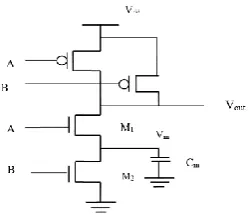
2.1. Calculation of Runtime Leakage Power A
technique has been suggested in literature [10] to calculate runtime leakage power. The leakage of logic gate depends on previous pattern and as well as on the time period. For example, the effect of leakage power on previous pattern at different time period for 2-input NAND gate (Figure 1) is shown in Table 1. When the previous pattern is 01, the internal node capacitor of capacitance Cm is totally discharged. After 10ns the when
the pattern is changed to 00 from 01, a small leakage current begins to charge node capacitor. Due to staking effect the leakage current through M1 drops as Vm rises.
The large turn on current through M1 starts charging Cm
and leakage current continues to charge Cm even when M1
turns off. If M1 turns on by the change of input from 00
to 01 Cm discharge quickly and leakage transition is
spontaneous.
Tables 1, 2 and 3 represents the runtime leakage power for 2 input NAND gate, 2 input NOR gate and NOT gate for all the possible combinations of input patterns.
TABLE 1. Runtime leakage power of 2 input NAND gate
TABLE 2. Runtime leakage power of 2 input NOR gate
Previous Pattern
Current
Pattern 10ns (nW) 20ns(nW)
40ns (nW)
00 01 80.94 78.40 77.60
00 10 80.39 75.50 73.38
00 11 70.80 68.02 66.84
01 00 79.58 77.69 77.15
01 10 49.87 46.69 45.07
01 11 0.006478 0.00522 0.004673
10 00 72.77 71.31 71.18
10 01 39.15 40.88 42
10 11 0.002972 0.002818 0.002779
11 00 65.57 64.86 65.68
11 01 0.6356 0.004057 0.2007
11 10 1.773 0.009718 0.5243
TABLE 3. Runtime leakage power of NOT gate
Previous Pattern
Current
Pattern 10ns(nW) 20ns(nW) 40ns(nW)
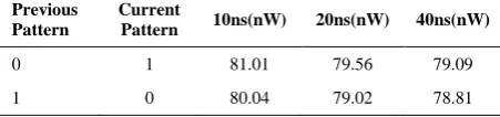
0 1 81.01 79.56 79.09
1 0 80.04 79.02 78.81
It is observed from the table that leakage power depends on previous pattern applied to the circuit and also changes with time period of simulation. Here leakage power is considered for three different time periods (10ns, 20ns and 40ns).
3. PROPOSED APPROACH FOR DON’T CARE FILLING AND ORDERING OF TEST PATTERNS
An approach based on Genetic Algorithm (GA) is used to fill up don’t cares present in test patterns and to reorder
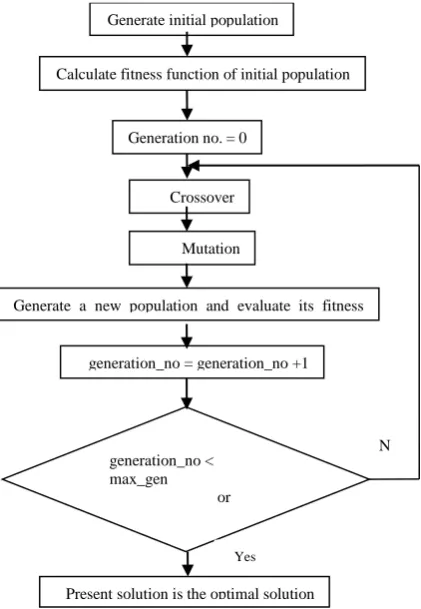
the patterns at a time so that the total power consumption is minimum. GA is used to create an initial population. Each population is encoded as a chromosome and fitness function of each chromosome is evaluated. The fitness of a chromosome determines its capability to survive and to create offspring. The population size is kept uniform throughout the generations.
Chromosome structure- Let the test patterns generated by –D 1 option of ATALANTA for C17.bench circuit are ‘100xx11’ (1st pattern), ‘00xxx1x’ (2nd
pattern), ‘xx101xx’ (3rd pattern), ‘0x1xx11’ (4th pattern),
‘1xx10111’ (5th pattern), ‘00x1x10’(6th pattern) and
‘001xx01’(7th pattern). Here, ‘x’ represents don’t care.
The number of don’t cares present in the set of test pattern is 19 and total number of test patterns generated is 7. The chromosome consists of two parts. One is ‘don’t care filling’ part which contains all the don’t cares that exists in the generated test patterns. The other part of chromosome is the ‘ordering of test patterns’ part which contains the number of test patterns generated by ATALANTA. Therefore the chromosome will look like:
1 0 0 1 1 0 1 0 1 1 0 1 0 0 0 1 0 1 1 5 4 2 7 1 6 3
Here the 5th pattern is applied first followed by 4th pattern,
2nd pattern and so on as seen in the chromosome structure.
Step 1: Generation of initial population- The first don’t care of the 5th pattern is substituted by the first bit
of chromosome. Correspondingly the next bit of the chromosome will replace the next X-bit of the next pattern and this continues until it reaches the last bit of chromosome.
Step 2: Calculation of fitness- Each chromosome represents one set of test pattern. As, we are targeting to minimize power without effecting fault coverage the cost function or fitness will consists of leakage and dynamic power.
Cost = Ptotal= Pdynamic + Pleakage
= αCLVdd2f + IlekVdd
where, supply voltage is Vdd, CL represents load
capacitance, α is the switching activity, f is the frequency of operation which is the inverse of critical delay of the circuit.
Value of CL and Ilek for all the gates are stored in
Look-up-Table (LUT) after simulation in CADENCE tool at 45nm technology and using supply voltage of 1V.
Step 3: Genetic operator-Here genetic operators are used to generate populations for next generation. The three operators of GA are selection, crossover and mutation.
A. Chromosome Selection - The chromosomes are
selected from the population based on fitness value for crossover, mutation and to produce offspring.
B. Crossover - It combines two chromosomes to produce
a new chromosome (offspring). The main idea of
Previous Pattern
Current
Pattern 10ns(nW) 20ns(nW) 40ns(nW)
00 01 0.54 0.002636 0.1296
00 10 2.059 1.102 0.5846
00 11 65.26 63.57 63.29
01 00 0.006477 0.00541 0.004932
01 10 54.32 51.52 50.10
01 11 81.84 79.09 78.16
10 00 0.003301 0.003087 0.003033
10 01 45.27 46.63 47.51
10 11 73.23 71.01 70.45
11 00 68.59 65.72 64.55
11 01 80.40 78.33 77.78
11 10 78.37 73.78 71.91
crossover is to get a new chromosome which may be better than both of the parents if it takes the best characteristics from each of the parents. Here we are using two point crossover. Consider the following crossover operation.
Parent 1:
Parent 2:
After crossover the offspring produced will be Offspring 1:
Offspring 2:
0 0 1 1 1 0 1 0 1 1 0 1 0 1 0 1 1 1 0 3 5 2 7 1 4 6
C. Mutation- 10% of the chromosomes gets mutated randomly and populate in the next generation. For mutation two sets of numbers s1, s2 (for ‘don’t care filling of test patterns’ part) and r1, r2 (for ‘ordering of test patterns’ part) are randomly generated. For ‘don’t care filling of test patterns’ part all the bits between s1 and s2 and changed 1 to 0 and from 0 to 1. For ‘ordering of test patterns’ part all the individual operand (oi) within r1 and r2 get changed with the (N-oi+1), where N is the number of patterns generated.
Here N is equal to 7. Therefore the operand 4 will be (7-4+1=4). So the operand 4 remains same. The next operand 7 will be (7-7+1=1). In this case 7 is replaced by 1. After mutation the chromosome becomes
Step 4: Termination- The steps for GA are repeated until there is no improvement in fitness function after 10 iterations
The steps for finding low power dissipation pattern considering integrated approach for don’t care filling and
ordering taking into account the previous pattern dependency using GA is summarized below:
a) An initial population is generated whose size is equal to the number of don’t care present in the test patterns and the number of test patterns generated.
b) The fitness function, of initial population is calculated according to leakage value in the LUT in Tables 1, 2 and 3.
c) For crossover a pair of parent chromosome is taken from current population based on the method described in literature [11].
d) Crossover is done by randomly chosen point to form two unique don’t care bits and test pattern ordering. e) Mutation is done for each bit of the chromosome and a unique filled don’t care bits and test pattern ordering is generated.
f) 80% of the newly generated test patterns and 20% of the existing test pattern are put in a new population. Now fitness function for new population is calculated. g) Repeat steps (c) to (f) for a number of generations till there is no improvement in values over last 40 generations.
i) Terminate the process and return the optimal solution. All the steps from a to i are repeated for different simulation time.
The flowchart of proposed algorithm is given in Figure 2.
4. EXPERIMENTAL RESULTS
Here we have considered ISCAS’85 benchmark circuits for our experiments. Test patterns with maximum fault coverage are generated with –D 1 option of ATALANTA. The existing don’t cares in the test patterns are filled and reordered simultaneously using GA considering runtime leakage power dependency on previous patterns and time period without effecting fault coverage. Runtime leakage power for 2 input NAND gate, 2 input NOR gate and NOT gate is calculated considering pattern dependency in ‘Cadence Virtuoso Analog Design Environment’ at 45 nm technology using supply voltage (Vdd) of 1 volt. The proposed method is
coded in C language. To reduce the size and complexity of the Look up Table (LUT) all the circuits are mapped into 2-input NAND gate, NOT gate and 2-input NOR gate using ABC tool. Table 4 shows the leakage power (cumulative) consumption for test patterns with don’t care filling and with default ordering, ordered test patterns (don’t care filling and then ordering of the filled patterns) and integrated approach for don’t care filling and ordering of test patterns considering different ISCAS’85 benchmark circuits. Table 4 consists of 5 columns. The first column shows the name of the benchmark circuits and the other columns show results for simulation at 10ns, 20ns, 40ns and 100ns time period. 1 0 0 1 1 0 1 0 1 1 0 1 0 0 0 1 0 1 1 5 4 2 7 1 6 3
0 0 1 1 1 0 1 0 0 1 0 1 0 1 0 1 1 1 0 3 5 7 2 1 4 6
1 0 0 1 1 0 1 0 0 1 0 1 0 0 0 1 0 1 1 5 4 7 2 1 6 3
1 0 0 1 1 1 0 1 1 0 1 0 1 0 0 1 0 1 1 5 4 1 6 7 2 3
1 0 0 1 1 0 1 0 0 1 0 1 0 0 0 1 0 1 1 5 4 7 2 1 6 3
D1 E1 F1
A1 B1 C1
A2 B2 C2 D2 E2 F2
A1 B2 C1 D1 E2 F1
A2 B1 C2 D2 E1 F2
r1 r2
S2 S1
Figure 2. Flowchart of the proposed algorithm
Except the first column the other column consists of three sub columns. The leakage power consumption for test patterns after don’t care filling and with default ordering is shown in the first sub column. The second sub column represents the results for test patterns after don’t care filing followed by ordering. The third sub column shows the results of proposed method for simultaneous don’t care filling and ordering of test patterns. Table 5 shows the % of leakage power savings after simultaneous don’t care filling and ordering of test patterns using GA compared to test patterns with default ordering. For C432 circuit the savings is 66.40% at 40ns and 66.36% at
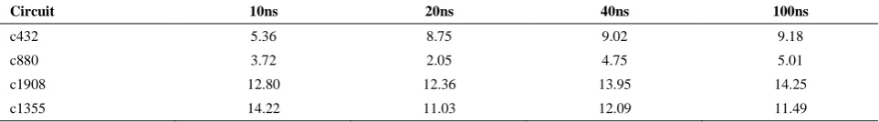
100ns. Table 6 shows the percentage of leakage power savings after simultaneous don’t care filling and ordering of test patterns at different time period compared to test patterns with don’t care filling followed by ordering. The cumulative power savings is 7.32% at 40ns and 7.39% at 100ns for C432 circuit. Table 7 shows the dynamic power for simultaneous ordering and filling of test patterns at different time period. It is observed that dynamic power also decreases using the proposed method. Table 8 shows the total power (dynamic and leakage power) consumption for test patterns after don’t care filling with ordering and after application of the integrated approach for don’t care filling and ordering of test patterns at four different time period. From Table 9 it can be seen that for C432 circuit the total power (dynamic and leakage power) savings is 9.02% at 40ns and 9.18% at 100ns. From the results the following observations can be made.
1. From Table 4 it is observed that test patterns with don’t care filling and with default ordering consumes maximum leakage power and as the time period increases this leakage power dependency on the ordering of the patterns gradually decreases. Also in general it is observed that as the time period increases the difference in the leakage power consumption compared to the previous time period decreases.
2. From Table 5 it is seen that compared to default ordering the leakage power savings is maximum for C432 circuit which is 66.40% at 40ns.
3. From Table 6 the maximum leakage power savings takes place for C1908 circuit at 100ns compared to don’t care filling followed by ordering of test patterns.
4. From Table 9 it is observed that the maximum savings in total power consumption is 14.25% for C1908 circuit at 100ns.
From the above observations it can be concluded that the integrated approach for don’t care filling and ordering of test patterns gives better results compared to don’t care filling with default ordering of test patterns and don’t care filling followed by ordering of test patterns.
TABLE 4. Cumulative leakage power for simultaneous ordering and filling of test patterns at different time period
10ns 20ns 40ns 100ns
Circuit
before ordering
of test patterns
(nW)
with ordering
of test patterns
(nW)
Proposed simultaneou
s ordering and filling of test patterns
(nW)
before ordering
of test patterns
(nW)
with ordering
of test patterns
(nW)
Proposed simultaneous ordering and filling of test patterns
(nW)
before ordering
of test patterns
(nW)
with ordering
of test patterns
(nW)
Proposed simultaneous ordering and filling of test patterns
(nW)
before ordering
of test patterns
(nW)
with ordering
of test patterns
(nW)
Proposed simultaneou
s ordering and filling of test patterns
(nW)
c432 7735.7 2770.8 2610.8 7353.7 2654.9 2589.5 7201.3 2610.3 2419.1 7133.1 2590.8 2399.1
c880 193749.9 105312.1 103171.0 185979.4 101101.4 100109.4 183156.3 99601.9 97511.8 181674.3 98808.4 96108.1
c1908 44229.3 34447.1 30176.2 43148.4 33630.6 29779.3 42837.1 33411.4 29114.9 42695.7 33313.7 28662.9
c1355 276229.6 198527.3 175652.4 268712.6 192109.6 174759.7 266518.4 190534.7 171964.5 265971.5 190187.8 169097.2 Generate initial population
Calculate fitness function of initial population
Generation no. = 0
Crossover
Mutation
Generate a new population and evaluate its fitness function
generation_no = generation_no +1
generation_no < max_gen
or no change of fitness
Present solution is the optimal solution
Yes
TABLE 5. Percentage of leakage saving after simultaneous don’t care filling and ordering of test patterns at different time period compared to default ordering of test patterns
Circuit 10ns 20ns 40ns 100ns
c432 66.25 64.78 66.40 66.36
c880 46.75 46.17 46.76 47.09
c1908 31.77 30.98 32.03 32.86
c1355 36.41 48.90 35.47 36.42
TABLE 6. Percentage of leakage saving after simultaneous ordering and filling of test patterns compared to reordering of test patterns
at different time period
Circuit 10ns 20ns 40ns 100ns
c432 5.77 2.46 7.32 7.39
c880 2.03 1.00 2.09 2.73
c1908 12.39 11.45 12.85 13.96
c1355 11.52 9.03 9.74 11.08
TABLE 7. Dynamic power for simultaneous ordering and filling of test patterns at different time period
10ns 20ns 40ns 100ns
Circuit
Dynamic power for don’t care filling and ordering
(nW)
Dynamic power for proposed method
(nW)
Dynamic power for don’t care filling and ordering
(nW)
Dynamic power for proposed method
(nW)
Dynamic power for don’t care filling and ordering
(nW)
Dynamic power for proposed method
(nW)
Dynamic power for don’t care filling and ordering
(nW)
Dynamic l power for proposed method
(nW)
c432 5512.68 5216.66 5878.27 5363.87 5298.89 4820.42 4990.42 4532.04
c880 211604.04 203720.08 199508.54 195398.67 194748.01 185497.47 191252.49 181670.74
c1908 69142.04 60286.03 59507.47 52152.34 58212.12 50091.52 57557.98 49355.96
c1355 406959.94 354502.80 345482.59 307378.86 341945.88 300604.62 333998.55 295622.11
TABLE 8. Total power consumption for proposed method
10ns 20ns 40ns 100ns
Circuit
Total power for don’t care filling and ordering
(nW)
Total power for proposed
method (nW)
Total power for don’t care filling and ordering
(nW)
Total power for proposed
method (nW)
Total power for don’t care filling and ordering
(nW)
Total power for proposed
method (nW)
Total power for don’t care filling and ordering
(nW)
Total power for proposed
method (nW)
c432 5512.68 5216.66 5878.27 5363.87 5298.89 4820.42 4990.42 4532.04
c880 211604.04 203720.08 199508.54 195398.67 194748.01 185497.47 191252.49 181670.74
c1908 69142.04 60286.03 59507.47 52152.34 58212.12 50091.52 57557.98 49355.96
c1355 406959.94 354502.80 345482.59 307378.86 341945.88 300604.62 333998.55 295622.11
TABLE 9. Percentage of total power savings after simultaneous ordering and filling of test patterns compared to don’t care filling and
ordering of test patterns at different time period
Circuit 10ns 20ns 40ns 100ns
c432 5.36 8.75 9.02 9.18
c880 3.72 2.05 4.75 5.01
c1908 12.80 12.36 13.95 14.25
5. CONCLUSION
In this paper an integrated approach based on genetic algorithm is used for don’t care filling and for ordering of test patterns considering pattern dependency. For our experiments we have considered ISCAS 85 benchmark circuits. Previous works on low power consumption concerns mainly about don’t care filling of test patterns or with don’t care filling and then ordering of test patterns. If reordering is done after don’t care filling then it will affect the optimum results obtained after don’t care filling. Considering the above issue we have proposed a method based on GA in which the chromosome consists of don’t care filling and ordering part. Considering the proposed method a maximum savings of 66.36% is obtained for C432 circuit compared to previous method.
6. ACKNOWLEDGEMENT
This work was supported by SMDP-C2SD project, sponsored by Deity, Govt. of India.
7. REFERENCES
1. Wang, S., "A bist tpg for low power dissipation and high fault coverage", IEEE Transactions on Very Large Scale Integration (VLSI) Systems, Vol. 15, No. 7, (2007), 777-789.
2. Wilson, L., "International technology roadmap for semiconductors (ITRS)", Semiconductor Industry Association, (2005).
3. Bushnell, M. and Agrawal, V., "Essentials of electronic testing for
digital, memory and mixed-signal vlsi circuits, Springer Science & Business Media, Vol. 17, (2000).
4. Shi, C. and Kapur, R., "How power-aware test improves reliability and yield", IEEDesign. com, September, Vol. 15, No., (2004).
5. Lin, Y.-S. and Sylvester, D., "Runtime leakage power estimation technique for combinational circuits", in Proceedings of the 2007 Asia and South Pacific Design Automation Conference, IEEE Computer Society., (2007), 660-665.
6. Kumar, S.K., Kaundinya, S., Kundu, S. and Chattopadhyay, S., "Particle swarm optimization based vector reordering for low power testing", in Computing Communication and Networking Technologies (ICCCNT), 2010 International Conference on, IEEE., (2010), 1-5.
7. Badereddine, N., Girard, P., Pravossoudovitch, S., Landrault, C., Virazel, A. and Wunderlich, H.-J., "Minimizing peak power consumption during scan testing: Test pattern modification with x filling heuristics", in Design and Test of Integrated Systems in Nanoscale Technology. DTIS 2006. International Conference on, IEEE., (2006), 359-364.
8. Kumar, S.K., Kaundinya, S., Kundu, S. and Chattopadhyay, S., "Customizing pattern set for test power reduction via improved x-identification and reordering", in Proceedings of the 16th ACM/IEEE international symposium on Low power electronics and design, ACM., (2010), 177-182.
9. Chattopadhyay, S. and Choudhary, N., "Genetic algorithm based approach for low power combinational circuit testing", in VLSI Design, 2003. Proceedings. 16th International Conference on, DOI: 10.1109/ICVD.2003.1183192, IEEE., (2003), 552-557. 10. Seomun, J., Shin, I. and Shin, Y., "Synthesis of active-mode
power-gating circuits", IEEE Transactions on Computer-Aided Design of Integrated Circuits and Systems, Vol. 31, No. 3, (2012), 391-403.
11. Choudhury, P. and Pradhan, S.N., "An approach for low power design of power gated finite state machines considering partitioning and state encoding together", Journal of Low Power Electronics, Vol. 8, No. 4, (2012), 452-463.
T. Sarkar*, S. Nath Pradhan
Department of ECE, National Institute of Technology, Agartala. Agartala, India
P A P E R I N F O
Paper history: Received 17 March 2017
Received in revised form 13 January 2018 Accepted 08 March 2018
Keywords: Testing Don’t Care Run Time Leakage Fault Coverage Genetic Algorithm Test Pattern Ordering Pattern Dependency
هديكچ
رادم ققحت رد یمهم راک ،شیامزآ نیح رد تردق للاحنا رثکادح ندناسر لقادح هب و دروآرب
VLSI
ریثأت اهرادم نانیمطا تیلباق رب تردق رادقم اریز ،تسا
اب هدش دیلوت تست یاهوگلا .دوش ذاختا قرب فرصم ندناسر لقادح هب یارب بسانم یاه شور دیاب شیامزآ نیح رد نیاربانب .دراذگ یم هنیزگ
-D 1
زا
ATALANTA
یواح
x
نیب زا .دناسرب لقادح هب ار یلاوتم یوگلا ود نیب ضیوعت یاه تیلاعف دادعت دناوت یمن تبقارم بسانم ندرک رپ اب .تسین مهم تیب
( نومزآ تحت رادم گنیچیئوس تردق نتفر
CUT
د نامز رگا .دراد یگتسب شیامزآ یارب هدافتسا دروم یاهوگلا بیترت هب زین ) هزادنا هب یلاوتم یوگلا تساوخر
گا اما ،دنک یمن رییغت تشن تردق طیارش نیا رد نیاربانب .دنک یمن رییغت اهوگلا یزاس بترم رد یتشن تردق نتفر نیب زا ،دشاب گرزب یفاک تساوخرد نامز ر
هب طوبرم لمعلاروتسد هب یگتسب ،دشاب کچوک یتشن یوگلا
CUT
دروم رد اهنت یلبق یاهراک .دراد زا سپ و دوش یمن ماجنا لوا ندرک رپ ای یوگلا ندرک رپ
ندرک رپ یایازم هک تسین مهم ،شرافس ندرک رپ زا سپ .دریگ یمن رارق هجوت دروم تردق مک رادم تست یارب نآ
X
تردق شهاک تست تیزم .دیهد رییغت ار
شور ود ره یجیردت
-کمه تروص رد دناوت یم یزاس بترم و ندرک رپ هک تسین مهم کیتنژ متیروگلا رب ینتبم یشور راک نیا رد .دوش هتفرگ رظن رد یرا
(
GA
ندرک رپ یارب لکشم هچراپکی لح یارب )
X
تیلاعف ندناسر لقادح هب روظنم هب یوگلا یگتسباو هب هجوت اب شیامزآ یاهوگلا هرابود یزاس بترم و
برثا .دوش یم هدافتسا اطخ ششوپ رییغت نودب تست رسارس رد گنیچیئوس رب ینتبم درکیور یشخ
GA
یشیامزآ یاهوگلا هب هجوت اب دوجوم درکیور اب هسیاقم رد
نومزآ یاهرادم
ISCAS'85
.تسا هدش هداد ناشن هجیتن شخب رد doi: 10.5829/ije.2018.31.05b.10