Low Power and Area EfficientALU Design
A.Sowmya, Dr.B.K.Madhavi
ABSTRACT:
This project work undertaken, aims at designing 8-bit ALU with carry select adder. An arithmetic logic unit acts as the basic building block or cell of a central processing unit of a computer. It is a digital circuit, compressed of the basic electronic components, which is used to perform various arithmetic, logic and integral operations. To design the power and area proficient fast speed data path logic systems, the field of very large scale integration (VLSI) is the generally significant area of research where minimize the area and power is the more difficult task. The carry select adder is the most suitable adder among the various adders.Most of the VLSI applications, such as DSP, image and video processing, and microprocessors use carry select adder (CSLA) for arithmetic functions. One of the existing solutions used in SQRT CSLA is replacement of second level RCA by BEC. Though increases the performance, very less percentage of improvement in reduction of area and power dissipation. An 8-bit ALU consists of carry select adders to reduce the ripple in design, and square root carry select adder is used in place of linear carry select adder to reduce propagation delay. The final 8 bit ALU can be designed with carry select adder.
(Keywords: Arithmetic Logic Unit(ALU), square root carry select adder(SQRT CSLA), ripple carry adder
(RCA).
I.INTRODUCTION
Design of any Low power VLSI circuit with less area and high speed has become a main concern for digital designers. Building low power VLSI systems has emerged as highly in demand because of the fast growing technology in mobile communications and computation. The battery technology does not advance at the same rate as microelectronics technology. There is a limited amount of power available for the mobile systems. So designers are faced with more constraints such as high speed, high throughput, small silicon area, and at the same time,
low power consumption. So building low power, high performance adder cells are of great interest.
The CSLA is used in many computational systems to alleviate the problem of carry propagation delay by independently generating multiple carries and then select a carry to generate the sum. However, the CSLA is not area efficient because it uses multiple pairs of Ripple Carry Adders (RCA) to generate partial sum and carry by considering carry input cin=0 and cin=1, then the final sum and carry are selected by the multiplexers (mux).
The basic idea of this work is to use Binary to Excess-1 Converter (BEC) instead of RCA with cin=1 in the regular CSLA to achieve lower area and power consumption. The main advantage of this BEC logic comes from the lesser number of logic gates than the n-bit Full Adder (FA) structure.
II. Regular 16-Bit SQRT CSLA
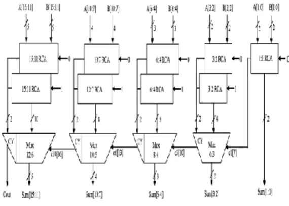
In digital adders, for speed up the operation Ripple Carry Adder (RCA) is modified as CSLA. To achieve more speed CSLA is replaced by SQRT CSLA. The CSLA is used in many computational systems to alleviate the problem of carry propagation delay by independently generating multiple carries and then select a carry to generate the sum. However, the CSLA is not area efficient because it uses multiple pairs of Ripple Carry Adders (RCA) to generate partial sum and carry input Cin=0 and Cin=1, the final sum and carry are selected by the multiplexers (mux).The structure of the 16-b regular SQRT CSLA is shown in Fig8. In general the complete SQRT CSLA is divided into different blocks. Block size and the number of blocks depend upon the size of SQRT CSLA according to the SQRT technique. From second block onwards, each block contains three different levels, first level is ripple carry adder with input carry zero, second level is ripple carry adder with input carry one and the third level is multiplexer which is used to select one of the ripple carry adders output according to the previous block carries. The disadvantage in SQRT CSLA is more area requirement as it uses two levels of RCAs.
Fig1.Regular 16-Bit SQRT CSLA
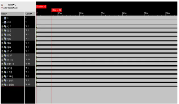
Simulation Results of Regular 16-bit
SQRT CSLA
Fig2. shows the regular 16-bit SQRT CSLA Simulation Results Respectively.
Fig 2 output waveform of regular 16-bit CSLA
II. Modified 16-bit SQRT CSLA
For achieving better area efficiency Binary to Excess-1 Converter (BEC instead of the RCA with cin =Excess-1 in order to reduce the area and power consumption of the regular CSLA. To replace the n bit RCA, an (n+1)-bit BEC is required. Second block of 16-bit SQRT CSLA with BEC logic.
One input of third level multiplexers is the output of first level RCA and another input is BEC output. This produces the two possible partial results in parallel and the multiplexer is used to select either the BEC output or the direct inputs according to the control signal cin.
Fig3.Modified 16-b SQRT CSLA. The parallel RCA with cin=1 is replaced with BEC.
Simulation Results of modified 16-bit
SQRT CSLA
Fig 4.shows the regular 16-bit SQRT CSLA Simulation Results Respectively.
Fig 4 output waveform of modified 16-bit CSLA
Comparison of Regular and Modified
SQRT CSLA
III.ALU with Carry Select Adder
1) Basic Concepts of ALU design
ALUs are implemented using lower-level components such as logic gates, including and, or,
not gates and multiplexers. These building blocks
work with individual bits, but the actual ALU works with 32-bit registers to perform a variety of tasks such as arithmetic and shift operations.In principle, an ALU is built from separate 1-bit ALUs. Typically, one constructs separate hardware blocks for each task (e.g., arithmetic and logical operations), where each operation is applied to the bits registers in parallel, and the selection of an operation is controlled by a multiplexer.
The advantage of this approach is that it is easy to add new operations to the instruction set, simply by associating an operation with a multiplexer control code. This can be done provided that the mux has sufficient capacity. Otherwise, new data lines must
be added to the mux (es), and the CPU must be modified to accommodate these changes.
2)Operation of ALU
The inputs of the circuit are: a = operand1
b = operand2
cin = carry in (we need that to do addition) The outputs of the circuit are:
result = outcome of the operation
cout = carry out (we need that to do addition). The circuit first computes all the possible outcomes: a+b, NOT(a), (a AND b), and (a OR b).
The desired result is then selected using a
multiplexor; the control signal of the multiplexor will be the operation code in the computer instruction.
Fig5. 1-bit ALU
We can construct a 4-bit ALU - an ALU that operates on 4 bit operands:
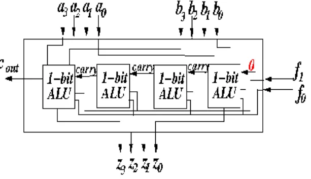
Fig6. 4-bit ALU
3) Carry Ripple ALU
Fig7 shows the 4 bit carry ripple ALU design, which is used for the design of 8 bit ALU CSLA and fig8 shows output of carry ripple ALU.
Fig7. 4-bit carry ripple ALU
Fig8.Output of carry ripple ALU
4) 8-Bit ALU with CSLA
Fig9. Shows 8bit ALU with 4bit CSLA. Here, 4 bit carry select refer to the size of the carry ripple units. An 8bit carry select would use 8 bit carry ripple units.
Fig9. 8bit ALU with 4bit CSLA Bits 7…4 Are Computed In Two Ways:
1) As if the carry in is a 0 2) As if the carry in is a 1
When actual carry in is known the correct result is selected.
Simulation Results of 8bit ALU with
CSLA
Fig 10 and fig 11 shows the 8bit ALU with CSLA schematicand simulation results respectively.
Fig11. Simulation output of 8-bit ALU with CSLA
Power report of 8bit ALU with CSLA:
Area(µm) Power(µw) 11832 29.015
IV.CONCLUSION
The existing ALU with carry select adder and its designing method in the VLSI design has been explained. Though these various designing method which explained in current work shows more proficient carry select adder having less area and lower power utilization than the other adders. Newer modification can focus on achieving more improved area-power-delay carry select adder for data processing processor in very large scale integration design.
References
[1] B. Ramkumar and Harish M Kittur, ―“Low
Power and Area-Efficient Carry Select Adder”
IEEE Transactions on Very Large Scale Integration (VLSI) Systems, VOL. 20, NO. 2, February 2012. [2] O. J. Bedrij, “Carry-select adder,” IRE Trans.
Electron. Comput., pp.340–344, 1962.
[3] B. Ramkumar, H.M. Kittur, and P. M. Kannan, “ASIC implementation of modified faster carry
save adder,” Eur. J. Sci. Res., vol. 42, no. 1, pp. 53–
58, 2010.
[4] T. Y. Ceiang and M. J. Hsiao, “Carry-select
adder using single ripple carry adder,” Electron.
Lett., vol. 34, no. 2o2, pp. 2101–2103, Oct. 1998.
[5] Y. Kim and L.-S. Kim,“64-bit carry-select adder
with reduced area,” Electron. Lett., vol. 37, no. 10,
pp. 614–615, May 2001.
[6] J. M. Rabaey,Digtal Integrated Circuits—A
Design Perspective. Upper Saddle River, NJ:
Prentice-Hall, 2001.
[7] Y. He, C. H. Chang, and J. Gu, “An area
efficient 64-bit square root carry-select adder for low power applications,” in Proc. IEEE Int.
Symp.Circuits Syst., 2005, vol. 4, pp. 4082–4085.
[8] Cadence, “Encounter user guide,” Version 6.2.4, March 2008.