Reliability Study of GaN-on-SiC HEMT RF Power Amplifiers
M. Bakowski
4,*, J. Lang
1, J-K. Lim
4, J. Hellén
3, T. M. J. Nilsson
3, B. Schodt
5,
R. Poder
5, I. Belov
2, P. Leisner
11
SP Technical Research Institute of Sweden, Box 857, 501 15 Borås, Sweden.
2
Jönköping University, School of Engineering, Box 1026, 551 11 Jönköping, Sweden.
3
Saab AB, Solhusgatan 10, 412 76 Gothenburg, Sweden.
4
RISE Acreo AB, Box 1070, 164 25 Kista, Sweden.
5
SP Technical Research Institute of Sweden, A.C. Meyers V. 15, 2450 Copenhagen, Denmark.
Received 21 July 2017; received in revised form 13 September 2017; accepted 19 September 2017
Abstract
The RF power amplifier demonstrators containing each one GaN-on-SiC, HEMT, CHZ015A-QEG, from UMS
in SMD quad-flat no-leads package (QFN) were subjected to thermal cycles (TC) and power cycles (PC) and
evaluated electrically, thermally and structurally. Two types of solders, Sn63Pb36Ag2 and lead-free SnAgCu
(SAC305), and two types of TIM materials, NanoTIM and TgonTM 805, for PCB attachment to the liquid cold plate
were tested for thermo-mechanical reliability. Changes in the electrical performance of the devices, namely the
reduction of the current saturation value, threshold voltage shift, increase of the leakage current and degradation of
the HF performance were observed as a result of an accumulated current stress during PC. No significant changes in
the investigated solder or TIM materials were observed.
Keywords: GaN-on SiC, HEMT, RF power amplifier, thermo-mechanical and electrical reliability
1.
Introduction
Radio frequency (RF) power amplifiers are used to convert a low-power signal into a higher power signal that drives the
antenna of a transmitter. There are two trends in the RF amplifier applications. The first is replacing silicon-based transistors,
such as LDMOS FETs, with GaN high electron-mobility power transistors (HEMT). This trend is observed, for example, in
telecom applications. The second trend is a transition from GaAs devices to GaN-on-SiC HEMTs, which is observed in the
applications with higher demands on output power and reliable high temperature operation, such as military applications. The
motivation for this study is the replacement of GaAs transistors with GaN-on-SiC devices in RF power amplifiers in order to
satisfy demands for higher output power, higher operating temperature (<200C) and higher system efficiency [1].
Reliability of WBG semiconductors and especially of GaN HEMTs is of primary importance and a subject of increasing
number of investigations [2-6]. The subject of investigations is most often devices themselves. The objectives of this
investigation are to experimentally investigate thermo-mechanical robustness of RF power amplifiers including packaged
HEMT devices assembled on PCB boards and exposed to power cycling (PC) and thermal cycling (TC) and to evaluate
prospective thermal management methods including thermal interface materials (TIM) by experiment and simulation. To
satisfy environmental demands, there is also need for investigation of thermo-mechanical behavior of modern lead-free solder
alloys in harsh environments.
*Corresponding author. E-mail address: [email protected]
2.
Experimental
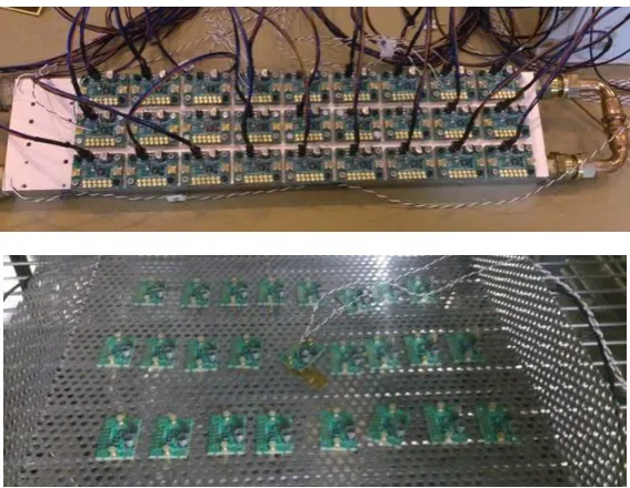
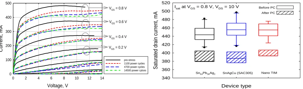
In total 50 RF amplifier demonstrators were assembled for the study. They consisted each of an 8 Cu-layer PCB board
with a simplified HF design containing one GaN-on-SiC, HEMT, CHZ015A-QEG, from UMS in SMD quad-flat no-leads
package (QFN). Two types of solders, Sn63Pb36Ag2 and lead-free SnAgCu (SAC305), and two types of TIM materials,
NanoTIM and TgonTM 805, for PCB attachment to the liquid cold plate were tested for thermo-mechanical reliability. In 8
Cu-layer PCB (25x35 mm) layers 2 and 7 contain solid Cu while layers 3 to 6 contain a 25% symmetrical Cu-layers with Daisy
Chains. The outer material is Ro4350 and material in-between Cu-layers is FR4. The transistor area (3.5x3.5 mm) is covered
by 0.3 wide Cu-plated vias distributed with 0.5 mm spacing center to center (Fig. 1). 24 demonstrators were subjected to
thermal stress by 2300 thermal cycles (TC) between -20°C and 80°C and remaining 26 were subjected to the electrical and
thermal stress by power cycling (PC) with drain current of 100 mA at a drain voltage of 45 V and cycle time of 2 min. HF
characterization of all the boards was done before subjecting them to the thermal and electrical stresses. All the devices were
also subjected to static electrical characterization by measuring threshold voltage and output and voltage blocking
characteristics. The static electrical and HF characterizations were performed again after 2300 cycles of TC stress and after
1100, 4700 and 14500 cycles of PC stress. In addition, failure analysis was performed on the TC and PC stressed
demonstrators by using optical microscopy and 2D X-ray microscopy.
(a) Cross-section (b) Top view
Fig. 1 RF amplifier demonstrators
The main reason for the TC tests was to test the reliability of the solder joints. The suggested tests were based on standard
IPC 785, treating HEMT devices and solder. One thermal cycle took 113 min. One month of the accelerated test is equal to
about one year of use in field conditions. The temperature in the chamber and the temperature on at least one board were
recorded during the whole test.
The main reason for the PC tests was to investigate degradation of the transistor package, including the die, solder joints
and TIM during cyclic heating and cooling. The temperature distribution on the HEMT package and PCB was measured
several times during the test by thermal imaging and by thermocouples. Power cycling was performed at room temperature
with demonstrator boards mounted on a liquid cold plate. The cycle time was set to 2 min and total number of cycles
corresponds to 20 years of use.
The boards were ID labeled and underwent a screening procedure under which some were visually inspected, powered up
and investigated with X-ray. After finishing TC and PC tests selected boards were visually inspected in white light, X-rayed
and a couple of boards were subjected to cross-section investigations for failure analysis.
3.
Results
The results of electrical and HF characterization show clearly changes and degradation in device performance as a
function of the number of the PC cycles and accumulated current stress time. An increase of the leakage current is observed
also after TC tests. No significant differences between the boards equipped with different solder and TIM materials were
observed which means that the observed changes in performance are due to the degradation of the HEMT devices.
3.1. PC tests
26 boards were mounted on a cold plate (water cooling with a flow of 0.015 l/s) with thermal paste between the Al-plate
of the demonstrator and the cold plate. The transistors were exposed to drain voltage of 45 V and a varying gate voltage of -1.9
V to – 3.0 V. At -1.9V the gate was opened yielding a drain current of ~100 mA. An equal on/off sequence of total 2 min was
repeated in total 14 500 times to correspond to 20 years of use. The 26 boards were divided into two groups connected in
parallel and run with one power supply per group. The experimental set-up is shown in Fig. 2.
3.1.1. Output characteristics
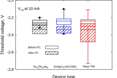
Typical output characteristics of the investigated devices are shown in Fig. 3 after various numbers of PC cycles. The
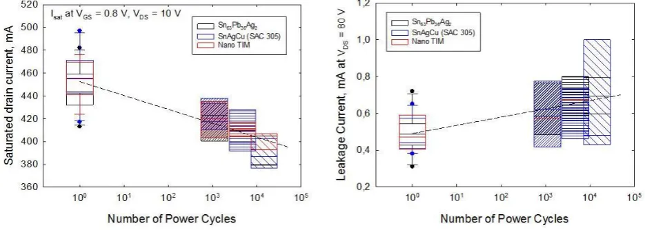
summary of values of saturated drain current before and after 14500 cycles of PC is shown in Fig. 4 for three groups of boards
having different solder and TIM materials (Sn63Pb36Ag2&Tgon805, SAC305&Tgon805 and SAC305&NanoTIM). The
saturated drain current values were taken for therain voltage VDS=10 V and gate voltage VGS=0.8 V. A reduction in value of the
saturation current is about 16 %, regardless of the type of the solder or TIM material used. The observed reduction in the value
of saturation current (VDS=10 V, VGS=0.8 V) is about 5, 12 and 16 % after 1100, 4700 and 14500 cycles of PC stress,
respectively.
Voltage, V
0 2 4 6 8 10 12 14
Cu rre n t, mA 0 100 200 300 400 500 pre-stress 1100 power cycles 4700 power cycles 14500 power cylces
VGS = 0.8 V
VGS = 0.6 V
VGS = 0.4 V
VGS = 0.2 V
Isat at VGS = 0.8 V, VDS = 10 V
Device type Sa tur ate d d rain c ur ren t, mA 340 360 380 400 420 440 460 480 500 520
Sn63Pb36Ag2 SnAgCu (SAC305) Nano TIM
Before PC After PC
Fig. 3 Typical output characteristics measured on the same device after various numbers of power cycles
The time dependence of the saturation current values is attributed to the degradation of the HEMT characteristics and is
discussed further in the discussion section below.
3.1.2. Threshold voltage shift
The threshold voltage was measured at VDS=45 V by sweeping gate voltage, VGS, from -7 V to 0 V. The threshold voltage
value was taken as a gate voltage corresponding to drain current IDS=10 mA. There is a clear tendency of the threshold voltage
shift towards more negative values showed by devices from different groups (Sn63Pb36Ag2&Tgon805, SAC305&Tgon805 and
SAC305&NanoTIM) as shown in Fig. 5. The shift is by -0.1 to -0.15 V from the typical value of about -2.25 V.
VTH at 10 mA
Device type
T
h
re
sho
ld vo
lt
a
g
e
, V
-2,8 -2,6 -2,4 -2,2 -2,0
Before PC After PC
Sn63Pb36Ag2 SnAgCu (SAC305) Nano TIM
Fig. 5 Threshold voltage values measured before and after 14500 cycles of PC stress
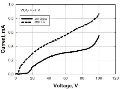
3.1.2. Leakage current
The leakage current is less well behaved. There are devices with relatively small change in leakage current but also
devices which show an increase in leakage current by a factor larger than 2, as a result of the PC stress. The typical forward
blocking characteristics of the devices after varying numbers of power cycles are shown in Fig. 6. The measurements were
done sweeping drain voltage, VDS, up to 100 V with gate voltage VGS=-7 V. The devices display high values of leakage current
with the relatively strong dependence on the drain voltage.
Fig. 6 Typical forward blocking characteristics of the investigated HEMT devices after consecutive series of power cycles (VGS=-7 V)
The summary of the leakage current data as a function of a number of power cycles is discussed in the discussion section
below.
3.2. TC tests
24 boards were exposed to 2300 temperature cycles of ∆T=100 °C between -20 °C to +80 °C in a temperature chamber.
boards had lead free solder material. The two kinds of boards (lead & lead free) were evenly mixed over the grid in the
chamber as shown in Fig. 2. The boards were electrically characterized before and after the thermal cycles.
3.2.1. Saturation current and threshold voltage
Figure 7 shows summary of saturated drain current and threshold voltage values for the boards with lead free solder.
Results show only minor changes after TC stress. The data for the reference boards with lead solder are very similar. These
changes could be possibly related to the deterioration of the solder joints, however, no change in the joints was observed when
performing material analysis. Visual inspection as well as 2D X-ray imaging was performed on all the thermally cycled
demonstrators. No failures related to the soldering were revealed during both TC and PC experiments.
Fig. 7 Saturated drain current value and threshold voltage value before and after TC stress
3.2.2. Leakage current
A significant increase of leakage current was observed in almost all the devices after the TC test as shown in Figs 8 and 9.
The mechanism behind this behavior is not clear.
Fig. 8 Typical blocking characteristics of the investigated HEMT devices before and after 2300 thermal cycles of TC
Fig. 9 Leakage current before and after 2300 cycles of TC stress
3.3. HF performance
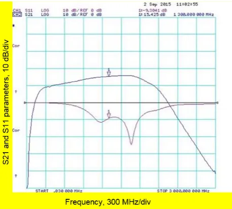
The RF measurements were performed using a Network Analyzer and registering S parameter values corresponding to
the frequency of 1.3 GHz as shown in Fig. 10. Results of HF measurements show a slight decrease in S11 (return loss) and S21
(gain) parameters from -10.91±0.23 to -10.0±0.21 and from 16.04±0.24 to 15.51±0.28, respectively, after PC stress
(measurement conditions VDS=45 V, IDS=100 mA, power level 5 dBm, 1.3 GHz). The summary of forward gain results (S21)
is presented in Fig. 11 and the summary of forward gain and return loss for SAC305 boards is shown in Fig. 12. Overall, the
high frequency measurements show a slight performance degradation of the power cycled boards and the same trend is
Fig. 10 Measurement of S21 (upper curve) and S11 (lower curve) parameters in the frequency range 30 kHz to 3 GHz
Fig. 11 Forward gain (S21) of boards with standard and lead-free solder before and after 14500 cycles of PC stress
Fig. 12 Forward gain (S21) and return loss (S11) of all boards with led-free solder before and after PC stress
3.4. Thermal modeling
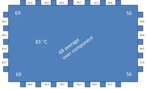
Temperature distribution measured with IR camera and result of CFD calculation are shown in Fig. 13 for dissipated
power of 7.2 W (steady state) with Tcoolant=11 °C, Tamb=21 °C. A good qualitative agreement has been obtained between
measurements and simulations. The coolant flow of 0.15-0.19 m/s is optimal for the set-up. Other simulation results are that
influence of using different solder materials is less than 1°C and that the newly developed NanoTIM results in 7°C lower
temperature compared to commercially available Tgon 805.
Validation of the transient CFD model is demonstrated in Fig. 14 and Fig. 15.
Fig. 14 Test board with attached thermocouples
Fig. 15 Simulated and measured temperature on chip and on PCB board (b) under TC pulse
The significant finding shown in Fig. 16 is that temperatures at different soldering locations of QFN HEMT package are
very different. It is important to take that into consideration when establishing and modeling reliability of soldered joints.
Fig. 16 Temperature at the QFN package and at PCB obtained from IR measurements
3.5. Material analysis
To reveal possible failures in solder joints, the packages were inspected with SEM and 2D X-ray, Fig. 17 and Fig. 18. No
obvious visual damage to the test PCBs was identified and no significant failure modes for the solder joints or component cases
Fig. 17 SEM images of a cross section of failed power cycled and thermally cycled devices with SAC 305
Fig. 18 2DX-ray images of a cross section of failed power cycled and thermally cycled devices with SAC 305
4.
Discussion
The electrical parameters that are clearly influenced by the PC are the saturation value of the drain current and leakage
current. The drain saturation and leakage currents of all the devices show logarithmic dependence on the stress time (number of
pulses), as can be seen in Figs 19 and 20. This is an indication that the changes are most probably related to charge trapping at
the near interfacial trapping sites located in the AlGaN layer or in the passivation layer. Assuming trapping sites are distributed
in distance from the specific interface and that charging is governed by the tunneling mechanism leads to the logarithmic
dependence of the accumulated charge on charging time [6]. This is because the charge transfer to the trapping sites becomes
less efficient, as trapping sites closest to the interface become occupied, due to exponentially decaying tunneling probability
with distance. The same time dependence is then reproduced by drain saturation current and leakage current given relatively
linear dependence of these two parameters on the interface charge.
Fig. 19 Saturated drain current value versus number of power cycles
Also TC has influence on leakage current as can be seen in Figs. 8 and 9. However no significant influence of the TC on
the remaining parameters was registered (Fig. 7). Investigated devices show high leakage currents and soft blocking
characteristics that seem to be easily influenced by thermal and electrical stress. Some of the experienced device failures are
most probably related to the device voltage blocking properties. In total 11 boards failed during the tests, 10 out of 26 tested
boards failed during the PC runs and 1 out of 24 tested boards failed during the TC run.
5.
Conclusions
Changes in electrical performance of the devices namely reduction of the drain current saturation value, threshold voltage
shift, increase of the leakage current and degradation of the HF performance were observed as result of an accumulated current
stress during PC tests. The most significant changes were observed in the drain saturation current and in the leakage current of
the devices. The changes in these two parameters seem to be logarithmic in time and indicate that the mechanism behind them
is charging of near interface states either in the AlGaN layer or in the passivation by tunneling.
A high rate of failures (40%) was observed in the PC tests. The failures are predominantly related to the same mechanism
that governs the increase of the leakage current. Also thermo-mechanical stress due to TC resulted in the increase of the
leakage current of the devices. No significant visual damages in the investigated solder or TIM materials were visually
observed in electron microscopy and 2D X-ray microscopy after PC and TC tests.
Acknowledgments
The support of Vinnova, Sweden´s innovation agency, and Sweden Energy Authority of this project with number
2014-05667, is acknowledged.
References
[1] U. K. Mishra, L. Shen, T. E. Kazior, and Y. F. Wu, “GaN-based RF power devices and amplifiers,” Proc. the IEEE, vol. 96, no. 2, pp. 287-305, February 2008.
[2] H. Kim, V. Tilak, B. M. Green, J. A. Smart, W. J. Schaff, J. R. Shealy, and L. F. Eastman, “Reliability evaluation of high power AlGaN/GaN HEMTs on SiC substrate,” Physica Status Solidi (a), vol. 188, no. 1, pp. 203-206, November 2001. [3] Y. C. Chou, D. Leung, I. Smorchkova, M. Wojtowicz, R. Grunbacher, L. Callejo, Q. Kan, R. Lai, P. H. Liu, D. Eng, and
A. Oki, “Degradation of AlGaN/GaN HEMTs under elevated temperature lifetesting,” Microelectronics Reliability, vol. 44, no. 7, pp. 1033-1038, July 2004.
[4] E. Zanoni, G. Meneghesso, M. Meneghini, A. Stocco, F. Rampazzo, R. Silvestri, I. Rossetto, and N. Ronchi, “Electric-field and thermally-activated failure mechanisms of AlGaN/GaN high electron mobility transistors,” ECS Transactions, vol. 41, no. 8, pp. 237-249, 2011.
[5] G. Meneghesso, M. Meneghini, D. Bisi, R. Silvestri, A. Zanandrea, O. Hilt, E. Bahat-Treidel, F. Brunner, A. Knauer, J. Wuerfl, and E. Zanoni, “GaN-based power HEMTs: parasitic, reliability and high field issues,” ECS Transactions, vol. 58, no. 4, pp. 187-198, 2013.
[6] A. Barnes, ESCCON 2013, 12-14 March 2013, ESA/ESTEC, Holland.