Adv. Radio Sci., 10, 327–332, 2012 www.adv-radio-sci.net/10/327/2012/ doi:10.5194/ars-10-327-2012
© Author(s) 2012. CC Attribution 3.0 License.
Advances in
Radio Science
Differential Algebraic Equations of MOS Circuits and Jump
Behavior
P. Sarangapani1, T. Thiessen2, and W. Mathis2 1Indian Institute of Technology, Madras, India
2Institute of Theoretical Electrical Engineering, Leibniz University of Hannover, Germany Correspondence to: T. Thiessen ([email protected])
Abstract. Many nonlinear electronic circuits showing fast switching behavior exhibit jump effects which occurs when the state space of the electronic system contains a fold. This leads to difficulties during the simulation of these systems with standard circuit simulators. A method to overcome these problems is by regularization, where parasitic inductors and capacitors are added at the suitable locations. However, the transient solution will not be reliable if this regulariza-tion is not done in accordance with Tikhonov’s Theorem. A geometric approach is taken to overcome these problems by explicitly computing the state space and jump points of the circuit. Until now, work has been done in analyzing exam-ple circuits exhibiting this behavior for BJT transistors. In this work we apply these methods to MOS circuits (Schmitt trigger, flip flop and multivibrator) and present the numerical results. To analyze the circuits we use the EKV drain current model as equivalent circuit model for the MOS transistors.
1 Introduction
In this work our focus lies on circuits which exhibit fast switching behavior (Schmitt Trigger, flip flop and multivi-brator). It is known that the derivative of the capacitor volt-ages and inductor currents govern the dynamics of an elec-tronic circuit. Also, the differential equations of elecelec-tronic circuits can be viewed as a flow on the state space mani-fold, which is represented by the algebraic constraints of the circuit. These circuits with discontinuous changes in states, which are called “jumps in state space”, contain a fold in their state space manifold. The simulation of these circuits leads to a simulation failure as the circuit can adopt multiple operating points at the same time. A method to overcome
this problem is to regularize the system by adding capaci-tors and induccapaci-tors at appropriate nodes, in accordance with Tikhonov’s theorem (Tikhonov et al., 1985). When the net-work is-regularized (Ihrig, 1975), the jump behavior can be viewed as the limit→0 of the solutions of the singularly perturbed system (Sastry and Desoer, 1981). This method can regularize the system, but it gives erroneous transient so-lutions by choosing wrongly located L’s and C’s. Another problem is due to the widely spaced time-constants, which appear because the dynamics of a regularized circuit can be divided into a slow and a fast part, leading to the so-called “time-constant problem” of circuit simulation (Sandberg and Shichman, 1968). Hence, we adopt a geometric approach and calculate the jump points and state space explicitly. This approach has been succesfully applied to example transistor circuits involving BJTs. In this work, we apply the method to MOS circuits and calculate the state space and jump points for Schmitt Trigger, flip flop and multivibrator and show that the results confirm with the simulation results. To efficiently model the MOS circuits, the EKV drain current model has been used (Enz et al., 1995).
2 Geometric interpretation of jump behavior
The state spaceS of an electronic circuit can be interpreted as a differentiable manifold and is given by the intersection of the OhmianOand the KirchhoffianKspaceS:=K∩O (Smale, 1972; Desoer and Wu, 1972; Chua, 1980). The dy-namics of an electronic circuit then is defined onS(Mathis, 1992). This implies that we need to satisfy the following conditions: (1)Sis a smooth manifold and (2) the dynamics can be created onS. The first is a typical or so-called generic condition (for a detailed discussion, see Mathis, 1992), and
in the following we assumeSto be a smooth manifold. The second condition requires the construction of a vector field
Xon the smooth manifoldS. Based on fundamental physi-cal laws, the relationships between currents and voltages of capacitors and inductors are given by means of differential relations. Therefore these differential equations are formu-lated iniLanduCcoordinate planes. Now, one has to “lift” or “pull-back” the dynamics on the state space S. There-fore, the vector field ceases to exist if the pull-back or the dynamics is degenerated, which leads to jumps inS. This degeneracy occurs ifScontains a fold. A detailed discussion of degeneracy can be found in Thiessen and Mathis (2011) and Mathis (1992).
If the circuit is characterized by the following algebro-differential equations (DAEs) in a semi explicit form:
˙
x=g(x,y,z) g:Rk→Rn (1)
0=f(x,y,z) f:Rk→Rm (2)
then the set of all jump points (jump-set) is characterized by J=det ∂yf(x,y,z)=0 wheref(x,y,z)=0. (3)
(see also Nielsen and Willson Jr. (1980), Tchizawa (1984), Ichiraku (1979),Thiessen et al. (2012)). The vectorx∈Rn corresponds to the capacitor voltages and inductor currents andy∈Rmis a vector of additional voltages and currents. Since there are circuits which exhibit a fold respectively their input voltages, we assign an additional vectorz∈Rη to dependent voltage or current input sources. We treat the in-dependent input sources as norators and assumezto be an-other variable in our system of equations. Therefore, the state spaceS of the circuit has to be extended by the number of independent sourcesη. Now, the dimensionkof the embed-ding spaceE∈Rk can be determined byk=n+m+ηand the dimension ofS bydim(S)=l=n+η. The state space Scan be defined as a subspace of theEand is represented by the solution set of the algebraic equations (2). The dynam-ical beahvior of the circuit is represented by the differential equations (1).
The jump takes place in a subspace parallel to the space spanned byy, whereyis the vector of all coordinates which are not fixed and do not conserve energy Thiessen and Mathis (2011), Thiessen et al. (2012). The corresponding “hit-set” is the intersection of the “bundle” of all jump spaces at points of the jump-set and the state spaceS.
To solve the equivalent circuits of the Schmitt Trigger, flip flop and multivibrator, we take this approach where we nu-merically calculate the jump points. For the determination of S, we interpretzas variables and by specifyinglcomponents ofy, we can calculateSThiessen et al. (2012).
3 Modelling the MOS equivalent circuit
It is known that the MOS drain current follows a square law and is a function of the gate-source and the drain-source
volt-ages and goes to zero belowVth. It is seen, that below the threshold voltage the current-voltage characteristic is expo-nential and is called as sub-threshold current and the behav-ior is as follows
Id=IS W
Lexp κV
gs UT
1−exp −V
ds UT
, (4)
whereUT is the thermal voltage, κ the non-ideality factor andIS is the saturation current. Since we are dealing with circuits that are switching from cutoff to saturation, we need a model that holds good for all regions of operation and does not exhibit the jump in the current function itself, as seen in the square law case. Hence, we use the EKV drain current equation, which is valid in all regimes. The following equa-tion shows the EKV current characteristic.
Id=2µnCox W
LU 2 Tln2
1+exp
V gs−Vt
2κUT
, (5)
whereκ is a variable and is adjusted according to the MOS under consideration. We can see that whenVgsis a significant value, the exponent dominates inside the logarithm and hence we can approximate ln(1+ex)uln(ex)=x. Upon using this
approximation we get
Id=
µnCox 2κ2
W
L Vgs−Vt 2
. (6)
If the gate source potential is a value comparable or less than
Vt, then we can approximate ln(1+ex)uex. With this
ap-proximation we get
Id=2µnCox W
LU 2 Texp
V gs−Vt
κUT
. (7)
Figure 1 illustrates how the EKV equation closely resembles the square law curve as well as the sub-threshold current in their respective regimes. The threshold voltage used for the analysis isVth=1.6 V. We compare the EKV model with the actual MOS (BSS123) that is going to be used for the sub-sequent analysis. From the parameters of the BSS123 MOS, we calculate the constants that need to be used in the EKV model. It gives us the following empirical drain current equa-tion, which can be used to simulate the circuits.
f (v)=a·ln2(1+exp(b(Vgs−1.6))) , (8) wherea=0.0013 andb=10.7250. Figure 2 shows the drain current versus the gate source voltage characteristic of the EKV approximation and the BSS123 forκ=1.8.
4 Example 1: Schmitt Trigger circuit
In this section we analyze the Schmitt Trigger circuit from a geometric point of view. The design parameters of the cir-cuit areRc1=2.5 k,Rc2=1 k,R1=10 k,R2=12 k,
P. Sarangapani et al.: DAEs of MOS Circuits and Jump Behavior
P. Sarangapani, T. Thiessen: Fast Switching Behaviour in MOS Circuits: A Geometric Approach
3293
1.4 1.42 1.44 1.46 1.48 1.5
0 0.5 1 1.5 2 2.5
3x 10
−5
Gate−Source Voltage (V)
Drain Current (A)
EKV model Sub−threshold current
(a) Sub-Threshold Case
1.4 1.6 1.8 2 2.2 2.4 2.6 2.8 3 0.1
0.2 0.3 0.4 0.5 0.6 0.7 0.8 0.9
Gate−Source Voltage (V)
Drain Current (A)
EKV model Square law
(b) Square-Law Case
Fig. 1: Comparison of the EKV model with the square
law and sub-threshold current
following empirical drain current equation, which can
be used to simulate the circuits.
f
(
v
) =
a
·
ln
2(
1
+
exp
(
b
(
V
gs−
1.6
)))
,
(8)
where
a
=
0.0013 and
b
=
10.7250. Fig.2 shows the drain
current versus the gate source voltage characteristic of
the EKV approximation and the BSS123 for
κ
=
1.8.
4
Example 1: Schmitt Trigger Circuit
In this section we analyze the Schmitt Trigger circuit
from a geometric point of view. The design parameters
of the circuit are
R
c1=
2.5
k
Ω
,
R
c2=
1
k
Ω
,
R
1=
10
k
Ω
,
R
2=
12
k
Ω
,
R
e=
300
Ω
,
U
o=
9
V
and
V
T=
1.6
V
. We
ne-glect the gate source capacitance during the calculation
of the jump points. These capacitances are used to
over-come the singular points and they aid in the
simula-tion of circuits with circuit simulators. In our approach,
addition of these regularization capacitances
C
Tis not
necessary. Eq.9 gives us the state space description of
the system.
U
inis the input and
U
gs1and
U
gs2are the
gate source voltages and are set as the state variables.
1.6 1.8 2 2.2 2.4 2.6 2.8 3 3.2 0
0.05 0.1 0.15 0.2 0.25 0.3 0.35 0.4 0.45 0.5
Gate−Source Voltage (V)
Drain Current (A)
BSS123 Model EKV Model
Fig. 2: Comparison of the EKV model with the BSS123
MOS
f
(
.
)
is the EKV equation as described in eq.8. The
out-put voltages are then found out as a function of
U
gs1,
U
gs2. The state space of the circuit is given by the
in-tersection of the solution sets of these two equations:
RC2
U0
RC1
R2
R1
UGS2
UGS1
I(UGS2)
I(UGS1)
Uout2
Uout1
Uin Re
Fig. 3: Schmitt Trigger Circuit
0
=
U
in1
R
e−
k
+
U
gs1k
−
1
R
e−
U
gs2k
+
f
(
U
gs1)
1
pR
1−
1
−
f
(
U
gs2)
−
pR
U
oc1
R
10
=
U
ink
−
U
gs1k
+
U
gs2k
−
f
(
U
gs1)
pR
1+
U
opR
c1R
1(9)
where the constants
p
and
k
are
p
=
1
R
c1+
1
R
1(10)
k
=
1
pR
21−
1
R
1−
1
R
2(11)
Fig. 1. Comparison of the EKV model with the square law and
sub-threshold current.
Re=300,Uo=9 V and VT=1.6 V. We neglect the gate source capacitance during the calculation of the jump points. These capacitances are used to regularize the circuit and therefore enable the simulation of the circuits with a common circuit simulator. In our approach, addition of these regular-ization capacitancesCTis not necessary. Equation (9) gives us the state space description of the system.Uinis the input andUgs1andUgs2are the gate source voltages and are set as the state variables.f (.)is the EKV equation as described in Eq. (8). The output voltages are then found out as a function ofUgs1,Ugs2. The state space of the circuit is given by the intersection of the solution sets of these two equations:
P. Sarangapani, T. Thiessen: Fast Switching Behaviour in MOS Circuits: A Geometric Approach
3
1.4 1.42 1.44 1.46 1.48 1.5
0 0.5 1 1.5 2 2.5
3x 10 −5
Gate−Source Voltage (V)
Drain Current (A)
EKV model Sub−threshold current
(a) Sub-Threshold Case
1.4 1.6 1.8 2 2.2 2.4 2.6 2.8 3
0.1 0.2 0.3 0.4 0.5 0.6 0.7 0.8 0.9
Gate−Source Voltage (V)
Drain Current (A)
EKV model Square law
(b) Square-Law Case
Fig. 1: Comparison of the EKV model with the square
law and sub-threshold current
following empirical drain current equation, which can
be used to simulate the circuits.
f
(
v
) =
a
·
ln
2(
1
+
exp
(
b
(
V
gs−
1.6
)))
,
(8)
where
a
=
0.0013 and
b
=
10.7250. Fig.2 shows the drain
current versus the gate source voltage characteristic of
the EKV approximation and the BSS123 for
κ
=
1.8.
4
Example 1: Schmitt Trigger Circuit
In this section we analyze the Schmitt Trigger circuit
from a geometric point of view. The design parameters
of the circuit are
R
c1=
2.5
k
Ω
,
R
c2=
1
k
Ω
,
R
1=
10
k
Ω
,
R
2=
12
k
Ω
,
R
e=
300
Ω
,
U
o=
9
V
and
V
T=
1.6
V
. We
ne-glect the gate source capacitance during the calculation
of the jump points. These capacitances are used to
over-come the singular points and they aid in the
simula-tion of circuits with circuit simulators. In our approach,
addition of these regularization capacitances
C
Tis not
necessary. Eq.9 gives us the state space description of
the system.
U
inis the input and
U
gs1and
U
gs2are the
gate source voltages and are set as the state variables.
1.6 1.8 2 2.2 2.4 2.6 2.8 3 3.2 0
0.05 0.1 0.15 0.2 0.25 0.3 0.35 0.4 0.45 0.5
Gate−Source Voltage (V)
Drain Current (A)
BSS123 Model EKV Model
Fig. 2: Comparison of the EKV model with the BSS123
MOS
f
(
.
)
is the EKV equation as described in eq.8. The
out-put voltages are then found out as a function of
U
gs1,
U
gs2. The state space of the circuit is given by the
in-tersection of the solution sets of these two equations:
RC2
U0 RC1
R2 R1
UGS2
UGS1
I(UGS2) I(UGS1)
Uout2 Uout1
Uin Re
Fig. 3: Schmitt Trigger Circuit
0
=
U
in1
R
e−
k
+
U
gs1k
−
1
R
e−
U
gs2k
+
f
(
U
gs1)
1
pR
1−
1
−
f
(
U
gs2)
−
pR
U
oc1
R
10
=
U
ink
−
U
gs1k
+
U
gs2k
−
f
(
U
gs1)
pR
1+
U
opR
c1R
1(9)
where the constants
p
and
k
are
p
=
1
R
c1+
1
R
1(10)
k
=
1
pR
21−
1
R
1−
1
R
2(11)
Fig. 2. Comparison of the EKV model with the BSS123 MOS.
P. Sarangapani, T. Thiessen: Fast Switching Behaviour in MOS Circuits: A Geometric Approach 3
1.4 1.42 1.44 1.46 1.48 1.5 0
0.5 1 1.5 2 2.5
3x 10
−5
Gate−Source Voltage (V)
Drain Current (A)
EKV model Sub−threshold current
(a) Sub-Threshold Case
1.4 1.6 1.8 2 2.2 2.4 2.6 2.8 3 0.1
0.2 0.3 0.4 0.5 0.6 0.7 0.8 0.9
Gate−Source Voltage (V)
Drain Current (A)
EKV model Square law
(b) Square-Law Case
Fig. 1: Comparison of the EKV model with the square law and sub-threshold current
following empirical drain current equation, which can be used to simulate the circuits.
f(v) =a·ln2(1+exp(b(Vgs−1.6))), (8)
wherea=0.0013 andb=10.7250. Fig.2 shows the drain current versus the gate source voltage characteristic of the EKV approximation and the BSS123 forκ=1.8.
4 Example 1: Schmitt Trigger Circuit
In this section we analyze the Schmitt Trigger circuit from a geometric point of view. The design parameters of the circuit are Rc1=2.5kΩ, Rc2=1kΩ, R1=10kΩ,
R2=12kΩ,Re=300Ω,Uo=9VandVT=1.6V. We
ne-glect the gate source capacitance during the calculation of the jump points. These capacitances are used to over-come the singular points and they aid in the simula-tion of circuits with circuit simulators. In our approach, addition of these regularization capacitancesCTis not
necessary. Eq.9 gives us the state space description of the system. Uinis the input andUgs1andUgs2are the
gate source voltages and are set as the state variables.
1.6 1.8 2 2.2 2.4 2.6 2.8 3 3.2
0 0.05 0.1 0.15 0.2 0.25 0.3 0.35 0.4 0.45 0.5
Gate−Source Voltage (V)
Drain Current (A)
BSS123 Model EKV Model
Fig. 2: Comparison of the EKV model with the BSS123 MOS
f(.)is the EKV equation as described in eq.8. The out-put voltages are then found out as a function ofUgs1,
Ugs2. The state space of the circuit is given by the
in-tersection of the solution sets of these two equations:
RC2
U0
RC1
R2
R1
UGS2
UGS1
I(UGS2)
I(UGS1)
Uout2
Uout1
Uin Re
Fig. 3: Schmitt Trigger Circuit
0=Uin
1 Re−k
+Ugs1
k− 1
Re
−Ugs2k
+f(Ugs1)
1
pR1−1
−f(Ugs2)−pRUo
c1R1
0=Uink−Ugs1k+Ugs2k−
f(Ugs1)
pR1 +
Uo
pRc1R1
(9)
where the constantspandkare
p= 1 Rc1
+ 1 R1
(10)
k= 1 pR21−
1
R1
− 1
R2 (11)
Fig. 3. Schmitt Trigger Circuit.
0=Uin 1
Re−k
+Ugs1
k− 1
Re
−Ugs2k +f (Ugs1)
1 pR1
−1−f (Ugs2)−pRUo c1R1 0=Uink−Ugs1k+Ugs2k−
f (Ugs1) pR1
+ Uo
pRc1R1
(9)
where the constantspandkare
p= 1
Rc1 + 1
R1
(10)
k= 1
pR12
− 1
R1 − 1
R2
(11) The system of equations is solved using Newton-Raphson method where the range ofUgs1is defined. To find the fold in the state space we need to choose a proper coordinate sys-tem. SinceUinis fixed, this state cannot jump. This implies that we need to look at theUin−Uout2curve for a fold. Fig-ure 4 indeed shows a fold and as expected, there are multiple
330 P. Sarangapani et al.: DAEs of MOS Circuits and Jump Behavior
4
P. Sarangapani, T. Thiessen: Fast Switching Behaviour in MOS Circuits: A Geometric Approach
The system of equations is solved using
Newton-Raphson method where the range of
U
gs1is defined.
To find the fold in the state space we need to choose
a proper coordinate system. Since
U
inis fixed, this
state cannot jump. This implies that we need to look
at the
U
in−
U
out2curve for a fold. Fig.4 indeed shows
a fold and as expected, there are multiple outputs for
the same input indicating singularity. To calculate the
point where the output transition occurs, we calculate
the jump points using the method as stated in eq.3. This
gives us
k
(
k
−
1
) +
f
0(
U
gs1)
1
pR
1−
1
−
k
+
f
0(
U
gs2)
k
+
f
0(
U
gs1)
pR
1=
0
(12)
To solve this equation we assume that
U
gs1varies
be-tween two predefined values and find
U
gs2. The points
intersecting with the solution set of the jump condition
and the state space, are defined as the jump points. The
jump points of the output are shown in Fig.4.
2 2.5 3 3.5 4 4.5 5 −2 0 2 4 6 8 10 Uin Uout2 Uout Uout−Jump
Fig. 4: Output vs. Input - Schmitt Trigger
5
Example 2: Flip Flop Circuit
This circuit is analyzed similar to the previous case.
This circuit is analytically similar to the Schmitt
Trig-ger, hence the results should be similar to the ones
ob-tained there. The following are the design parameters
of the circuit:
U
o=
9
V
,
V
T=
1.6
V
,
R
c1=
10
Ω
,
R
c2=
10
Ω
,
R
b1=
10
k
Ω
,
R
b2=
10
k
Ω
,
R
x=
10
k
Ω
,
R
y=
10
k
Ω
and
R
v=
5
k
Ω
. The equations governing the circuit are
0
=
U
0qR
b1R
c2−
k
−
1qR2
b1
U
gs1−
f
(
U
gs2)
qR
b1+
U
inR
v0
=
U
0pR
c1R
b2+
1
pR
2b2−
1
R
b2−
1
R
x!
U
gs2−
f
(
U
gs1)
pR
b2(13)
RC2 U0 RC1 Uin Rx Ry Rb2 Rb1 RV UGS2 UGS1I(UGS2) I(UGS1)
Uout2 Uout1
Fig. 5: Flip Flop Circuit
where the constants
k
,
p
,
q
are
k
=
1
R
b1+
1
R
v+
1
R
y(14)
p
=
1
R
c1+
1
R
b2(15)
q
=
1
R
c2+
1
R
b1(16)
where
U
inis the input,
U
out2is the output and
U
gs1,
U
gs2are the gate source voltages of the MOS. The phase
space and the jump points are obtained by declaring
U
gs1between two predefined values and solving for
U
gs2for that corresponding value of
U
gs1. The jump
condition here turns out to be
1
R
2b1q
−
k
!
1
pR
2b2−
1
R
b2−
1
R
x−
f
0(
U
gs1
)
f
0(
U
gs2)
pqR
b1R
b2=
0
(17)
The jump points of the output are shown in Fig.6.
6
Example 3: Multivibrator
In the earlier sections the systems of equations were
only algebraic ones. Here, for the multivibrator, we
get a semi explicit DAE system. The device parameters
chosen for this circuit are:
U
o=
5
V
,
V
T=
1.6
V
,
R
1=
5
k
Ω
,
R
2=
100
k
Ω
,
C
=
33
nF
,
I
o=
0.26
mA
. The
equa-tions governing this circuit are:
0
=
U
0R
1−
U
gs1R
1+
R
22
+
U
gs2R
22
R
1(
R
1+
R
2)
+
I
0R
1R
2−
U
c(
R
1+
R
2)
2
R
1(
R
1+
R
2)
−
f
(
U
gs2)
Fig. 4. Output vs. Input – Schmitt Trigger.
outputs for the same input indicating singularity. To calculate the point where the output transition occurs, we calculate the jump points using the method as stated in Eq. (3). This gives us
k(k−1)+f0(Ugs1) 1
pR1 −1
− k+f0(Ugs2)
k+f 0
(Ugs1) pR1
=0
(12)
To solve this equation we assume thatUgs1 varies between two predefined values and findUgs2. The intersections of the solution set of Eq. (12) and the state space are defined as the jump points. The jump points of the output are shown in Fig. 4 as the intersection of both curves.
5 Example 2: Flip Flop circuit
The flip flop circuit is analyzed similar to the previous case. This circuit is analytically similar to the Schmitt Trigger, hence the results should be similar to the ones obtained there. The following are the design parameters of the circuit:
Uo=9 V,VT=1.6 V,Rc1=10,Rc2=10,Rb1=10 k, Rb2=10 k,Rx=10 k,Ry=10 kandRv=5 k. The
equations governing the circuit are 0= U0
qRb1Rc2 −
k− 1
qRb12
Ugs1−
f (Ugs2) qRb1
+Uin
Rv
0= U0
pRc1Rb2
+ 1
pRb22
− 1
Rb2 − 1
Rx
! Ugs2−
f (Ugs1) pRb2
(13) where the constantsk,p,q are
k= 1
Rb1 + 1 Rv + 1 Ry (14)
p= 1
Rc1 + 1
Rb2
(15)
4 P. Sarangapani, T. Thiessen: Fast Switching Behaviour in MOS Circuits: A Geometric Approach
The system of equations is solved using Newton-Raphson method where the range of Ugs1 is defined.
To find the fold in the state space we need to choose a proper coordinate system. Since Uin is fixed, this
state cannot jump. This implies that we need to look at theUin
−
Uout2curve for a fold. Fig.4 indeed showsa fold and as expected, there are multiple outputs for the same input indicating singularity. To calculate the point where the output transition occurs, we calculate the jump points using the method as stated in eq.3. This gives us
k
(
k−
1) +
f0(
Ugs1)
1 pR1
−
1
−
k+
f0(
Ugs2)
k
+
f0
(
Ugs1)
pR1
=
0(12)
To solve this equation we assume thatUgs1 varies
be-tween two predefined values and findUgs2. The points
intersecting with the solution set of the jump condition and the state space, are defined as the jump points. The jump points of the output are shown in Fig.4.
2 2.5 3 3.5 4 4.5 5 −2 0 2 4 6 8 10 Uin Uout2 Uout Uout−Jump
Fig. 4: Output vs. Input - Schmitt Trigger
5 Example 2: Flip Flop Circuit
This circuit is analyzed similar to the previous case. This circuit is analytically similar to the Schmitt Trig-ger, hence the results should be similar to the ones ob-tained there. The following are the design parameters of the circuit: Uo
=
9V,VT=
1.6V, Rc1=
10Ω, Rc2=
10Ω, Rb1
=
10kΩ,Rb2=
10kΩ,Rx=
10kΩ,Ry=
10kΩandRv
=
5kΩ. The equations governing the circuit are0
=
U0qRb1Rc2
−
k
−
1qR2
b1
Ugs1
−
f
(
Ugs2)
qRb1
+
UinRv
0
=
U0pRc1Rb2
+
1pR2b2
−
1 Rb2−
1 Rx!
Ugs2
−
f
(
Ugs1)
pRb2
(13) RC2 U0 RC1 Uin Rx Ry Rb2 Rb1 RV UGS2 UGS1
I(UGS2)
I(UGS1)
Uout2
Uout1
Fig. 5: Flip Flop Circuit
where the constantsk,p,qare
k
=
1Rb1
+
1Rv
+
1Ry (14)
p
=
1Rc1
+
1Rb2
(15)
q
=
1Rc2
+
1Rb1
(16)
whereUinis the input,Uout2is the output andUgs1,Ugs2
are the gate source voltages of the MOS. The phase space and the jump points are obtained by declaring Ugs1 between two predefined values and solving for
Ugs2 for that corresponding value of Ugs1. The jump
condition here turns out to be
1 R2b1q
−
k!
1 pR2b2
−
1 Rb2
−
1 Rx
−
f 0(
Ugs1
)
f0(
Ugs2)
pqRb1Rb2
=
0(17)
The jump points of the output are shown in Fig.6.
6 Example 3: Multivibrator
In the earlier sections the systems of equations were only algebraic ones. Here, for the multivibrator, we get a semi explicit DAE system. The device parameters chosen for this circuit are: Uo
=
5V,VT=
1.6V,R1=
5kΩ,R2
=
100kΩ,C=
33nF,Io=
0.26mA. Theequa-tions governing this circuit are:
0
=
U0R1
−
Ugs1
R1
+
R22
+
Ugs2R22 R1
(
R1+
R2)
+
I0R1R2
−
Uc(
R1+
R2)
2
R1
(
R1+
R2)
−
f(
Ugs2)
Fig. 5. Flip Flop Circuit.q= 1
Rc2 + 1
Rb1
. (16)
Uinis the independent input voltage,Uout2is the output and Ugs1,Ugs2are the gate source voltages of the MOS. The state space and the jump points are obtained by declaring Ugs1 between two predefined values and solving forUgs2for that corresponding value ofUgs1. The determinant criterion here turns out to be
1
R2b1q−k !
1
pR2b2−
1
Rb2− 1
Rx
−f 0(U
gs1)f0(Ugs2) pqRb1Rb2
=0
(17)
The jump points of the output are shown in Fig. 6 as the intersection of both curves.
6 Example 3: multivibrator
In the earlier sections the systems of equations were only algebraic ones. Here, for the multivibrator, we get a semi explicit DAE system. The device parameters chosen for this circuit are: Uo=5 V,VT=1.6 V,R1=5 k,R2=100 k, C=33 nF,Io=0.26 mA. The equations governing this cir-cuit are:
0=
U0R1−Ugs1
R1+ R2
2
+Ugs2R2 2
R1(R1+R2) +
I0R1R2−
Uc(R1+R2) 2
R1(R1+R2)
−f (Ugs2)
0=
U0R1+ Ugs1R2
2 −Ugs2
R1+ R2
2
R1(R1+R2) +
Uc(R1+R2)
2 +I0R1R2
R1(R1+R2)
−f (Ugs1)
P. Sarangapani et al.: DAEs of MOS Circuits and Jump Behavior 331
P. Sarangapani, T. Thiessen: Fast Switching Behaviour in MOS Circuits: A Geometric Approach
5
−2 0 2 4 6 8 10
−4 −2 0 2 4 6 8
Uin
Uout2
Uout2 Uout2−Jump
Fig. 6: Output vs. Input - Flip Flop
R
1R
1U
0C
I(U
GS1)
I(U
GS2)
R
2R
2I
0I
0U
GS1U
GS2Fig. 7: Multivibrator Circuit Diagram
0
=
U
0R
1+
U
gs1R
22
−
U
gs2R
1+
R
22
R
1(
R
1+
R
2)
+
U
c(
R
1+
R
2)
2
+
I
0R
1R
2R
1(
R
1+
R
2)
−
f
(
U
gs1)
˙
U
c=
−
U
c2
−
R
2f
(
U
gs1) +
R
2f
(
U
gs2)
CR
2−
R
2
U
gs12
−
R
2U
gs22
+
R
2U
c2
CR
1R
2(18)
The above equations can be written in a matrix form as
0
0
˙
U
c
=
g
(
U
gs1,
U
gs2,
U
c)
(19)
The state space of the circuit is given by the
intersec-tion of the surfaces
S
1and
S
2, where
S
1is the solution
set of
g
1(
U
gs1,
U
gs2,
U
c) =
0 and
S
2is the solution set
of
g
2(
U
gs1,
U
gs2,
U
c) =
0. Fig.8 shows the intersection
of the two surfaces. The intersection curve (in blue)
is the state space of the circuit. The state space has
to be plotted in a coordinate system, where one of the
quantity does not jump whereas the other two show
jump behavior. Hence the state space was plotted in
U
gs1−
U
gs2−
U
ccoordinate system. The jump criterion
for this circuit is given as
R
1+
R
22
2R
1(
R
1+
R
2)
−
R
22
R
1(
R
1+
R
2)
−
f
0(
U
gs1
)
·
·
R
22
R
1(
R
1+
R
2)
−
f
0
(
U
gs2
)
=
0
(20)
Upon solving this with Newton-Raphson method we
Fig. 8: State space of multivibrator circuit
get the jump points as shown in Fig.9. The jump points
are shown in the
U
gs1−
U
gs2coordinate system as jump
occurs only for these two voltages. Fig.10, on the other
hand shows the jump behaviour in the
U
gs1−
U
gs2−
U
ccoordinate system. We can see that jump occurs in
the direction where the capacitance potential
U
cis
con-served. This happens as the capacitance potential
can-not jump instantaneously.
7
Conclusion
Analysis of electronic circuits that contain a fold in
their state space with common circuit simulators like
SPICE sometimes gives errors due to time constant
problems. The analysis of these circuits require
regu-larization, which is achieved by adding capacitors and
inductors at appropriate nodes. If the regularization is
not done in accordance with Tikhonov’s theorem, the
transient solutions will not be reliable. With our
ap-proach regularization is no longer necessary as it is
pos-Fig. 6. Output vs. Input – Flip Flop.
P. Sarangapani, T. Thiessen: Fast Switching Behaviour in MOS Circuits: A Geometric Approach 5
−2 0 2 4 6 8 10 −4
−2 0 2 4 6 8
Uin
Uout2
Uout2 Uout2−Jump
Fig. 6: Output vs. Input - Flip Flop
R1 R1
U0
C
I(UGS1) I(UGS2)
R2 R2
I0 I0
UGS1 UGS2
Fig. 7: Multivibrator Circuit Diagram
0= U0R1+
Ugs1R2
2 −Ugs2
R1+
R2
2
R1(R1+R2)
+
Uc(R1+R2)
2 +I0R1R2
R1(R1+R2)
−f(Ugs1)
˙
Uc=−
U
c
2 −R2f(Ugs1) +R2f(Ugs2)
CR2
−
R
2Ugs1
2 −
R2Ugs2
2 +
R2Uc
2
CR1R2
(18)
The above equations can be written in a matrix form as
0 0 ˙
Uc
=g(Ugs1,Ugs2,Uc) (19)
The state space of the circuit is given by the intersec-tion of the surfacesS1andS2, whereS1is the solution
set ofg1(Ugs1,Ugs2,Uc) =0 andS2 is the solution set
ofg2(Ugs1,Ugs2,Uc) =0. Fig.8 shows the intersection
of the two surfaces. The intersection curve (in blue) is the state space of the circuit. The state space has to be plotted in a coordinate system, where one of the quantity does not jump whereas the other two show jump behavior. Hence the state space was plotted in
Ugs1−Ugs2−Uccoordinate system. The jump criterion
for this circuit is given as
R1+
R2
2
2
R1(R1+R2)−
R2
2R1(R1+R2)−f
0(Ugs
1)
·
·
R2
2R1(R1+R2)
−f0(Ugs2)
=0
(20)
Upon solving this with Newton-Raphson method we
Fig. 8: State space of multivibrator circuit
get the jump points as shown in Fig.9. The jump points are shown in theUgs1−Ugs2coordinate system as jump
occurs only for these two voltages. Fig.10, on the other hand shows the jump behaviour in theUgs1−Ugs2−Uc
coordinate system. We can see that jump occurs in the direction where the capacitance potentialUcis con-served. This happens as the capacitance potential can-not jump instantaneously.
7 Conclusion
Analysis of electronic circuits that contain a fold in their state space with common circuit simulators like SPICE sometimes gives errors due to time constant problems. The analysis of these circuits require regu-larization, which is achieved by adding capacitors and inductors at appropriate nodes. If the regularization is not done in accordance with Tikhonov’s theorem, the transient solutions will not be reliable. With our ap-proach regularization is no longer necessary as it is
pos-Fig. 7. Multivibrator Circuit Diagram.
˙
Uc= − U
c
2 −R2f (Ugs1)+R2f (Ugs2)
CR2
− R
2Ugs1
2 −
R2Ugs2
2 +
R2Uc 2
CR1R2
(18)
The above equations can be written in a matrix form as
0 0 ˙
Uc
=h(Ugs1,Ugs2,Uc) (19)
The state space of the circuit is given by the intersec-tion of the surfaces S1 and S2, where S1 is the solution set of h1(Ugs1,Ugs2,Uc)=0 and S2 is the solution set of h2(Ugs1,Ugs2,Uc)=0. Figure 8 shows the intersection of the two surfaces. The intersection curve (in blue) is the state space of the circuit. The state space has to be plotted in a coordinate system, where one of the quantity does not jump whereas the other two show jump behavior. Hence the state
P. Sarangapani, T. Thiessen: Fast Switching Behaviour in MOS Circuits: A Geometric Approach
5
−2 0 2 4 6 8 10
−4 −2 0 2 4 6 8
Uin
Uout2
Uout2 Uout2−Jump
Fig. 6: Output vs. Input - Flip Flop
R
1R
1U
0C
I(U
GS1)
I(U
GS2)
R
2R
2I
0I
0U
GS1U
GS2Fig. 7: Multivibrator Circuit Diagram
0
=
U
0R
1+
U
gs1R
22
−
U
gs2R
1+
R
22
R
1(
R
1+
R
2)
+
U
c(
R
1+
R
2)
2
+
I
0R
1R
2R
1(
R
1+
R
2)
−
f
(
U
gs1)
˙
U
c=
−
U
c2
−
R
2f
(
U
gs1) +
R
2f
(
U
gs2)
CR
2−
R
2
U
gs12
−
R
2U
gs22
+
R
2U
c2
CR
1R
2(18)
The above equations can be written in a matrix form as
0
0
˙
U
c
=
g
(
U
gs1,
U
gs2,
U
c)
(19)
The state space of the circuit is given by the
intersec-tion of the surfaces
S
1and
S
2, where
S
1is the solution
set of
g
1(
U
gs1,
U
gs2,
U
c) =
0 and
S
2is the solution set
of
g
2(
U
gs1,
U
gs2,
U
c) =
0. Fig.8 shows the intersection
of the two surfaces. The intersection curve (in blue)
is the state space of the circuit. The state space has
to be plotted in a coordinate system, where one of the
quantity does not jump whereas the other two show
jump behavior. Hence the state space was plotted in
U
gs1−
U
gs2−
U
ccoordinate system. The jump criterion
for this circuit is given as
R
1+
R
22
2R
1(
R
1+
R
2)
−
R
22
R
1(
R
1+
R
2)
−
f
0(
U
gs1)
·
·
R
22
R
1(
R
1+
R
2)
−
f
0
(
U
gs2
)
=
0
(20)
Upon solving this with Newton-Raphson method we
Fig. 8: State space of multivibrator circuit
get the jump points as shown in Fig.9. The jump points
are shown in the
U
gs1−
U
gs2coordinate system as jump
occurs only for these two voltages. Fig.10, on the other
hand shows the jump behaviour in the
U
gs1−
U
gs2−
U
ccoordinate system. We can see that jump occurs in
the direction where the capacitance potential
U
cis
con-served. This happens as the capacitance potential
can-not jump instantaneously.
7
Conclusion
Analysis of electronic circuits that contain a fold in
their state space with common circuit simulators like
SPICE sometimes gives errors due to time constant
problems. The analysis of these circuits require
regu-larization, which is achieved by adding capacitors and
inductors at appropriate nodes. If the regularization is
not done in accordance with Tikhonov’s theorem, the
transient solutions will not be reliable. With our
ap-proach regularization is no longer necessary as it is
pos-Fig. 8. State space as intersection ofS1andS2.
space was plotted inUgs1−Ugs2−Uccoordinate system. The determinant criterion for this circuit is given as
R1+
R2 2
2 R1(R1+R2)
− R2
2R1(R1+R2)
−f0(Ugs1)
·
·
R
2 2R1(R1+R2)
−f0(Ugs2)
=0
(20)
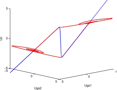
Upon solving this with Newton-Raphson method we get the jump points as shown in Fig. 9. The jump points are shown in theUgs1−Ugs2coordinate system as the intersection of both curves. For verifying our results we regularized the system of equations by adding regularization capacitances parallel toUgs1andUgs2. The transient behavior of this regularized circuit can be seen in Fig. 10 (red line). We can see that the fast transition occurs in theUgs1andUgs2space, where the capacitance potentialUcis hold mostly constant.
7 Conclusions
The simulation of electronic circuits that contain a fold in their state space with common circuit simulators like SPICE sometimes gives errors due to time constant problems. The analysis of these circuits require regularization, which is achieved by adding capacitors and inductors at appropriate nodes. If the regularization is not done in accordance with Tikhonov’s Theorem, the transient solutions will not be re-liable. With our approach, regularization is no longer nec-essary, as it is possible to detect whether the manifold of the circuit’s state space has a fold beforehand. The jump points, therefore help us to identify the points of transition easily. We have shown numerical results of applying the geometric concepts to three MOS circuits. Therefore, the MOS drain current was modelled using the EKV equation for robust results.
3326 P. Sarangapani, T. Thiessen: Fast Switching Behaviour in MOS Circuits: A Geometric ApproachP. Sarangapani et al.: DAEs of MOS Circuits and Jump Behavior
1.35 1.4 1.45 1.5 1.55 1.6 1.65 1.25
1.3 1.35 1.4 1.45 1.5 1.55 1.6
Ugs1
Ugs2
Ugs2 Ugs2−JP
Fig. 9: Jump points inUgs1−Ugs2coordinate system
−5 0
5 −5
0
5 −5
0 5
Ugs1 Ugs2
Uc
Fig. 10: Jump Behaviour inUgs1−Ugs2−Uccoordinate
system
sible to detect whether the manifold of the circuit’s state space has a fold beforehand. The jump points, there-fore help us to identify the points of transition easily. We have shown numerical results of applying the geo-metric concepts to three MOS circuits. The MOS drain current is modeled using the EKV equation for robust results.
Acknowledgment
The authors would like to thank the German Re-search Foundation (DFG) and the German Academic Exchange Service (DAAD) for the financial support.
References
Chua, L.: Dynamic nonlinear networks: State-of-the-art, IEEE Transactions on Circuits and Systems, CAS-27, 1059–1087,
1980.
Desoer, C. and Wu, F.: Trajectories of nonlinear RLC net-works: A geometric approach, IEEE Transactions on Cir-cuit Theory, 19, 562 – 571, 1972.
Enz, C. C., Krummenacher, F., and Vittoz, E. A.: An analyt-ical MOS transistor model valid in all regions of opera-tion and dedicated to low-voltage and low-current appli-cations, Analog Integr. Circuits Signal Process., 8, 83–114, 1995.
Ichiraku, S.: Connecting Electrical Circuits: Transversality and Well-Posedness, Yokohama mathematical Journal, 27, 111–126, 1979.
Ihrig, E.: The Regularization of Nonlinear Electrical Circuits, Proceedings of the American Mathematical Society, 47, pp. 179–183, 1975.
Mathis, W.: Geometric theory of nonlinear dynamical net-works, in: Computer Aided Systems Theory EUROCAST – ’91, edited by Pichler, F. and Díaz, R., vol. 585 ofLecture Notes in Computer Science, pp. 52–65, Springer Berlin / Hei-delberg, 1992.
Nielsen, R.O. and Willson, A.N., Jr.: A fundamental result concerning the topology of transistor circuits with multiple equilibria, Proc. of the IEEE, 68, 196 – 208, 1980.
Sandberg, I. W. and Shichman, H.: Numerical integration of systems of stiff nonlinear differential equations, Bell Syst. Tech. J., 47, 511–527, 1968.
Sastry, S. and Desoer, C.: Jump behavior of circuits and sys-tems, Circuits and Syssys-tems, IEEE Transactions on, 28, 1109 – 1124, doi:10.1109/TCS.1981.1084943, 1981.
Smale, S.: On the mathematical foundation of electrical circuit theory, Journ. Differential Geometry, 7, 193–210, 1972. Tchizawa, K.: An Analysis of Nonlinear Systems with
Re-spect to Jump, Yokohama mathematical Journal, 32, 203– 214, 1984.
Thiessen, T. and Mathis: Geometric Dynamics of Nonlinear Circuits and Jump Effects, International Journal of Com-putations & Mathematics in Electrical & Electronic Engi-neering (Compel 2011), 30, 1307–1318, 2011.
Thiessen, T., Gutschke, M., Blanke, P., Mathis, W., and Wolter, F.-E.: A Numerical Approach for Nonlinear Dynamical Circuits with Jumps, in: 20th European Conference on Cir-cuit Theory and Design (ECCTD 2011), 2011.
Thiessen, T., Plönnigs, S., and Mathis, W.: A Geometric MNA Based Approach for Circuits with Fast Switching Behavior (presented), 2012 IEEE International Symposium on Cir-cuits and Systems (ISCAS 2012), 2012.
Tikhonov, A. N., Vasil’eva, A. B., and Sveshnikov, A. G.: Dif-ferential Equations, Springer-Verlag, Berlin-Heidelberg-New York-Tokyo, 1985.
Fig. 9. Jump points in theUgs1−Ugs2coordinate system. 1.35 1.4 1.45 1.5 1.55 1.6 1.65 1.25
1.3 1.35 1.4 1.45 1.5 1.55 1.6
Ugs1
Ugs2
Ugs2 Ugs2−JP
Fig. 9: Jump points inUgs1−Ugs2coordinate system
−5 0
5 −5
0
5 −5
0 5
Ugs1 Ugs2
Uc
Fig. 10: Jump Behaviour inUgs1−Ugs2−Uc coordinate
system
sible to detect whether the manifold of the circuit’s state space has a fold beforehand. The jump points, there-fore help us to identify the points of transition easily. We have shown numerical results of applying the geo-metric concepts to three MOS circuits. The MOS drain current is modeled using the EKV equation for robust results.
Acknowledgment
The authors would like to thank the German Re-search Foundation (DFG) and the German Academic Exchange Service (DAAD) for the financial support.
References
Chua, L.: Dynamic nonlinear networks: State-of-the-art, IEEE Transactions on Circuits and Systems, CAS-27, 1059–1087,
1980.
Desoer, C. and Wu, F.: Trajectories of nonlinear RLC net-works: A geometric approach, IEEE Transactions on Cir-cuit Theory, 19, 562 – 571, 1972.
Enz, C. C., Krummenacher, F., and Vittoz, E. A.: An analyt-ical MOS transistor model valid in all regions of opera-tion and dedicated to low-voltage and low-current appli-cations, Analog Integr. Circuits Signal Process., 8, 83–114, 1995.
Ichiraku, S.: Connecting Electrical Circuits: Transversality and Well-Posedness, Yokohama mathematical Journal, 27, 111–126, 1979.
Ihrig, E.: The Regularization of Nonlinear Electrical Circuits, Proceedings of the American Mathematical Society, 47, pp. 179–183, 1975.
Mathis, W.: Geometric theory of nonlinear dynamical net-works, in: Computer Aided Systems Theory EUROCAST – ’91, edited by Pichler, F. and Díaz, R., vol. 585 ofLecture Notes in Computer Science, pp. 52–65, Springer Berlin / Hei-delberg, 1992.
Nielsen, R.O. and Willson, A.N., Jr.: A fundamental result concerning the topology of transistor circuits with multiple equilibria, Proc. of the IEEE, 68, 196 – 208, 1980.
Sandberg, I. W. and Shichman, H.: Numerical integration of systems of stiff nonlinear differential equations, Bell Syst. Tech. J., 47, 511–527, 1968.
Sastry, S. and Desoer, C.: Jump behavior of circuits and sys-tems, Circuits and Syssys-tems, IEEE Transactions on, 28, 1109 – 1124, doi:10.1109/TCS.1981.1084943, 1981.
Smale, S.: On the mathematical foundation of electrical circuit theory, Journ. Differential Geometry, 7, 193–210, 1972. Tchizawa, K.: An Analysis of Nonlinear Systems with
Re-spect to Jump, Yokohama mathematical Journal, 32, 203– 214, 1984.
Thiessen, T. and Mathis: Geometric Dynamics of Nonlinear Circuits and Jump Effects, International Journal of Com-putations & Mathematics in Electrical & Electronic Engi-neering (Compel 2011), 30, 1307–1318, 2011.
Thiessen, T., Gutschke, M., Blanke, P., Mathis, W., and Wolter, F.-E.: A Numerical Approach for Nonlinear Dynamical Circuits with Jumps, in: 20th European Conference on Cir-cuit Theory and Design (ECCTD 2011), 2011.
Thiessen, T., Plönnigs, S., and Mathis, W.: A Geometric MNA Based Approach for Circuits with Fast Switching Behavior (presented), 2012 IEEE International Symposium on Cir-cuits and Systems (ISCAS 2012), 2012.
Tikhonov, A. N., Vasil’eva, A. B., and Sveshnikov, A. G.: Dif-ferential Equations, Springer-Verlag, Berlin-Heidelberg-New York-Tokyo, 1985.
Fig. 10. Transient solution (red) of the regularized circuit in the Ugs1−Ugs2−Uc coordinate system; state space of non-regularized circuit (blue).
Acknowledgements. The authors would like to thank the German
Research Foundation (DFG) and the German Academic Exchange Service (DAAD) for the financial support.
References
Chua, L.: Dynamic nonlinear networks: State-of-the-art, IEEE T. Circuits Syst., CAS-27, 1059–1087, 1980.
Desoer, C. and Wu, F.: Trajectories of nonlinear RLC networks: A geometric approach, IEEE T. Circuit Syst., 19, 562–571, 1972.
Enz, C. C., Krummenacher, F., and Vittoz, E. A.: An analytical MOS transistor model valid in all regions of operation and dedi-cated to low-voltage and low-current applications, Analog Integr. Circuits Signal Process., 8, 83–114, 1995.
Ichiraku, S.: Connecting Electrical Circuits: Transversality and Well-Posedness, Yokohama Mathematical Journal, 27, 111–126, 1979.
Ihrig, E.: The Regularization of Nonlinear Electrical Circuits, P. Am. Math. Soc., 47, 179–183, 1975.
Mathis, W.: Geometric theory of nonlinear dynamical networks, in: Computer Aided Systems Theory EUROCAST – ’91, edited by: Pichler, F. and D´ıaz, R., vol. 585 of Lecture Notes in Computer
Science, 52–65, Springer Berlin/Heidelberg, 1992.
Nielsen, R. O. and Willson Jr., A. N.: A fundamental result con-cerning the topology of transistor circuits with multiple equilib-ria, Proc. of the IEEE, 68, 196–208, 1980.
Sandberg, I. W. and Shichman, H.: Numerical integration of sys-tems of stiff nonlinear differential equations, Bell Syst. Tech. J., 47, 511–527, 1968.
Sastry, S. and Desoer, C.: Jump behavior of circuits and systems, IEEE T. Circuits Syst., 28, 1109–1124, doi:10.1109/TCS.1981. 1084943, 1981.
Smale, S.: On the mathematical foundation of electrical circuit the-ory, J. Differ. Geom., 7, 193–210, 1972.
Tchizawa, K.: An Analysis of Nonlinear Systems with Respect to Jump, Yokohama Mathematical Journal, 32, 203–214, 1984. Thiessen, T. and Mathis: Geometric Dynamics of Nonlinear
Cir-cuits and Jump Effects, International Journal of Computations & Mathematics in Electrical & Electronic Engineering (Compel 2011), 30, 1307–1318, 2011.
Thiessen, T., Gutschke, M., Blanke, P., Mathis, W., and Wolter, F.-E.: A Numerical Approach for Nonlinear Dynamical Circuits with Jumps, in: 20th European Conference on Circuit Theory and Design (ECCTD 2011), 2011.
Thiessen, T., Pl¨onnigs, S., and Mathis, W.: Transient Solution of Fast Switching Systems without Regularization, in: IEEE 55th International Midwest Symposium on Circuits and Systems (MWSCAS 2012), 578–581, 2012.
Tikhonov, A. N., Vasil’eva, A. B., and Sveshnikov, A. G.: Differ-ential Equations, Springer-Verlag, Berlin-Heidelberg-New York-Tokyo, 1985.